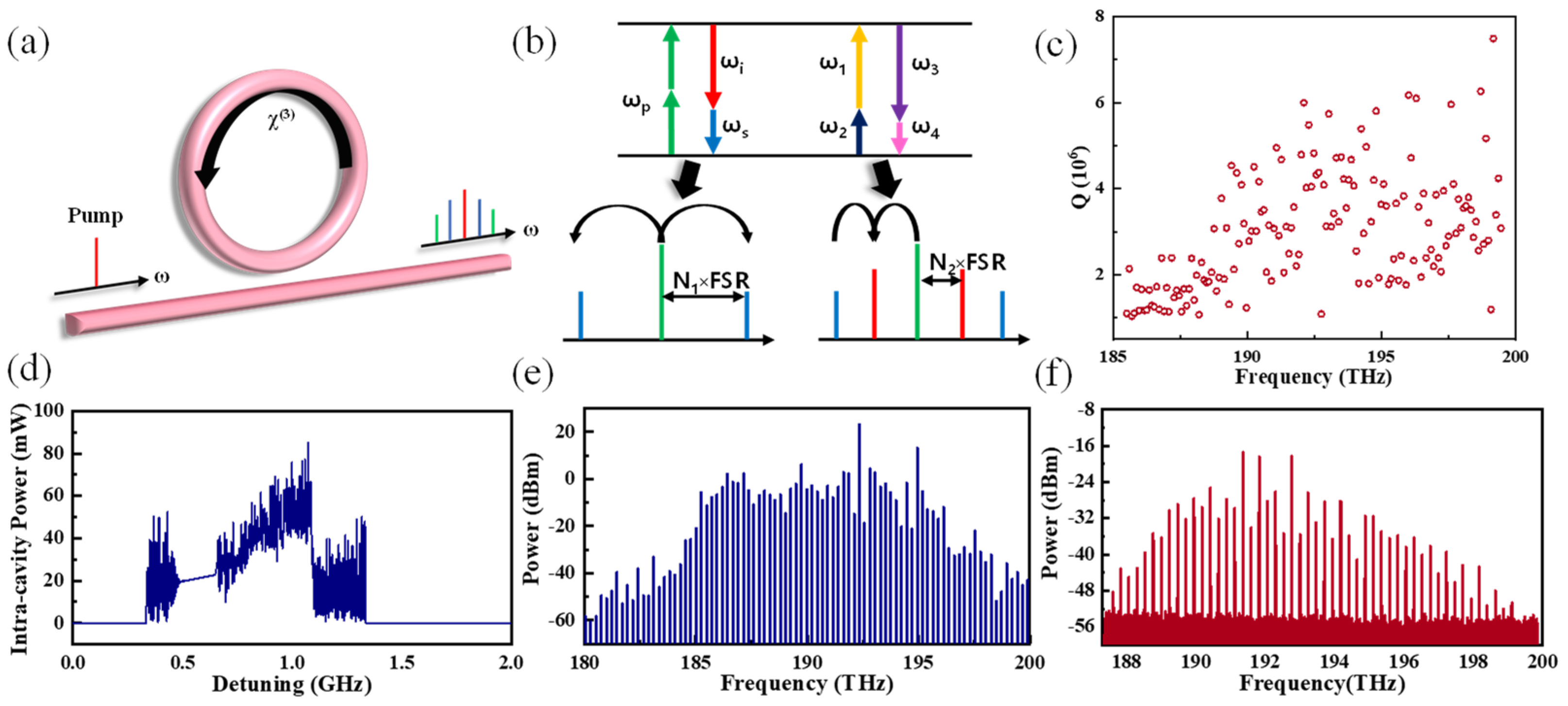
1. Introduction
In the rapidly evolving landscape of photonic integrated circuits (PICs), silicon nitride (SiN) stands out as a leading material due to its exceptional properties, such as ultralow optical losses [
1], absence of two-photon absorption in telecommunication bands [
2], strong Kerr nonlinearity and high-power handling capability [
3,
4]. These attributes make SiN an ideal candidate for a wide range of applications, including delay lines [
5], chip-scale frequency combs [
6,
7,
8], and narrow-linewidth lasers [
9], particularly when implemented with thick SiN waveguides [
10]. The use of thick SiN layers enhances optical confinement, reduces scattering losses and can engineer dispersion, which is advantageous for producing anomalous group velocity dispersion (GVD) [
11,
12,
13,
14,
15,
16,
17,
18,
19,
20]. Building in the properties, in 2016, M. H. P. Pfeiffer et al. constructed a micro-resonator with a radius of 238 μm, comprising waveguides with dimensions of 1.35 μm in height and 1.5 μm in width. This resonator exhibited an optical quality (Q) factor of 3.7 × 10
6. Leveraging the high-Q SiN micro-resonator with anomalous GVD, the researchers were able to generate a broadband frequency comb through the mechanism of single temporal dissipative Kerr soliton (DKS), as reported in reference [
21].
Plasma-enhanced chemical vapor deposition (PECVD) and low-pressure chemical vapor deposition (LPCVD) are two key techniques to produce SiN films. While PECVD can produce thicker SiN films, it is associated with reduced film uniformity compared to LPCVD. The SiN film produced by PECVD has a higher hydrogen bond concentration, approximately 20% [
22,
23,
24], which results in optical absorption within the C-band, primarily due to N-H and Si-H bonds [
12,
25], increasing optical losses and adversely affecting device performance. In contrast, LPCVD produces a SiN film with greater uniformity and lower hydrogen bond content, which is beneficial for improving the performance of SiN photonic devices. However, the fabrication of thick LPCVD SiN films, particularly on larger wafers (6 inches or larger), presents significant challenges [
26]. The increased thickness can induce high stress levels that can lead to cracking, a phenomenon that constrains dispersion-based photonic devices to smaller wafers [
27]. This restricts the scalability and cost-effectiveness of photonic devices, as larger wafers are more economical for mass production.
To address these challenges, researchers have implemented various stress management strategies, including the incorporation of stress-relief layers and optimizing deposition and etching processes [
4,
24].
Table 1 lists out a comparison of SiN waveguide processing methods tailored to various wafer sizes and film thicknesses. In a notable advancement, Dirani et al., in 2019, succeeded in depositing thick SiN films on 8-inch wafers using an optimized conventional subtractive process [
25]. To control strain and prevent cracking, they deposited SiN films in two or more LPCVD steps. Between each of the two deposition steps, the carrier wafer had to be rotated by 45° to distribute the uniaxial strain over the entire film thickness. The low loss of the waveguides was obtained, which contributed to the annealing process in special ambient conditions to drive out the residual polymer and N-H bonds, resulting in an ultra-smooth sidewall. However, this work places a high dependency on the equipment used, which is not commonly available in foundries. An alternative approach to prevent film cracking is the damascene process, which was initially developed for semiconductor metal interconnects and later adapted for SiN photonics. This process structures the substrate before depositing the SiN film and then planarizes it, effectively managing stress and preventing cracking [
11,
25]. The process has provided a fundamental solution to the challenges associated with thick SiN film fabrication, paving the way for advanced photonic chips on a wafer scale [
4,
26].
Despite the success of the damascene process, there have been few reports of its applications on larger wafers, such as 8-inch wafers, while most research and development focused on smaller wafer sizes [
26,
27]. Scaling up to larger wafers introduces additional complexities, such as maintaining uniformity and controlling stress distribution across the entire wafer [
28,
29,
30].
Table 1.
Summary of the SiN waveguide processing platforms.
Table 1.
Summary of the SiN waveguide processing platforms.
| Research Team | Wafer Size
(inch) | Deposition Method | Cross-Sectional Size (μm2) |
|---|
| Ying Huang [31] | 8 | PECVD | 0.4 × 1.0 |
| Sheng Chun Mao [32] | 8 | PECVD | 0.4 × 0.7 |
| Zhendong Zhu [27] | 6 | LPCVD | 0.4 × 1.8 |
| Ling Hua Wang [33] | 4 | PECVD | 0.6 × 1.5 |
| Clemens J. Krückel [34] | 4 | LPCVD | 0.7 × 1.65 |
| Jörn P. Epping [26] | 4 | LPCVD | 0.9 × 1.2 |
| Tobias Kippenberg [4] | 4 | LPCVD | 0.9 × 2.1 |
| Zhichao Ye [35] | 3 | LPCVD | 0.74 × 1.5 |
| Houssein El Dirani [25] | 8 | LPCVD | 0.8 × 1.5 |
| This paper | 8 | LPCVD | 0.8 × 0.8 |
In this work, we have successfully executed a damascene fabrication technique to fabricate SiN photonic devices with a thickness of 0.8 μm on an 8-inch wafer, which effectively addresses the issue of cracking. The waveguide loss is systematically characterized, with wafer-level test results showing a mean propagation loss of less than 0.33 dB/cm. Simultaneously, a 2 × 2 multimode interference (MMI) coupler is designed, and its performance is experimentally validated, demonstrating a low excess loss of −0.1 dB and an imbalance of 0.06 dB. Furthermore, micro-ring resonators with varying widths are engineered, and their transmission spectra and Q factors are characterized and analyzed. The findings indicate that micro-resonators with wider widths can achieve higher Q factor, exceeding 1 × 10⁶, which facilitates the generation of frequency combs.
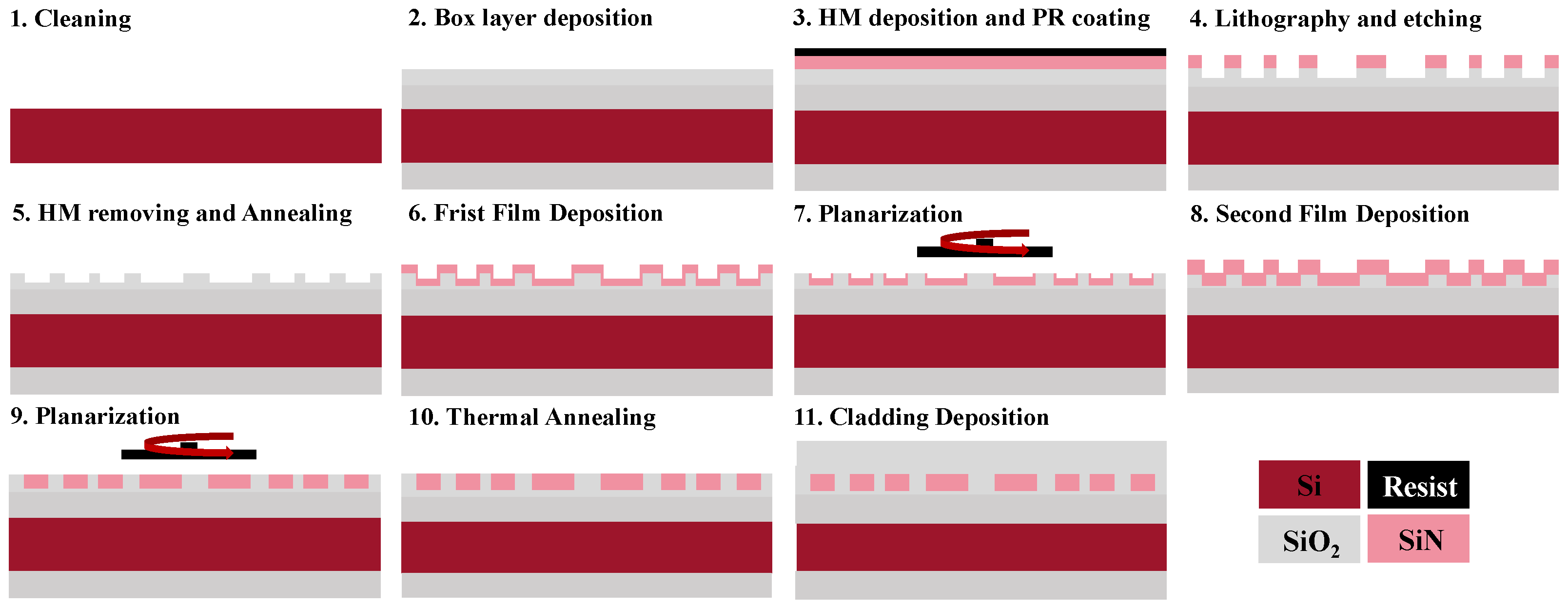
2. Fabrication Process
Our designed devices are fabricated by KrF (248 nm) Deep Ultraviolet (DUV) lithography with our developed photonic damascene process on an 8-inch wafer. The suggested fabrication process flow of the SiN devices on an 8-inch CMOS pilot line is shown in
Figure 1.
After cleaning the wafer, a 4 μm-thick SiO2 layer served as the lower cladding and was deposited through a combination of thermal oxidation and PECVD processes to a silicon wafer. In detail, a 3 μm SiO2 film was grown by a thermal oxygen process with an annealing temperature of ~1100 °C, and then the 1 μm SiO2 film was deposited by the PECVD process. This not only saves the time of growing 1 μm by the thermal oxygen process, but also obtains the easily etched SiO2 film provided by the PECVD process. The SiO2 film prepared by the thermal oxygen process has a low hydrogen content, and the furnace tube process is used to grow the film on both sides of the wafer, so the wafer is basically not deformed after the film is grown, and the stress limit is well controlled.
On top of the SiO2 layer, ~330 nm-thick SiN film is deposited by PECVD, acting as a hard mask (HM) for the subsequent SiO2 etching process and the photoresist (PR) was coated on top of the HM. This ensures that the critical dimensions of the lithography step remain unchanged and the sidewall roughness of the lower SiO2 cladding trench is greatly improved. Following DUV lithography and etching steps, SiO2 grooves matching the device’s dimensions were etched into the lower cladding. Subsequently, the grooves were refluxed with an annealing process in a furnace with temperature of ~1100 °C for ≥7 h to reduce sidewall roughness and residual O-H bonds within the lower cladding. To form the SiN core layer, a two-step deposition method was employed using LPCVD. After the first SiN deposition, a chemical mechanical polishing (CMP) process was used to remove excess SiN film outside the grooves, effectively reducing the film strain. High-temperature annealing was then carried out to release Si-H and N-H bonds in the SiN core layer, significantly reducing absorption losses in the thin film. A 2.6-μm-thick SiO2 layer was deposited by PECVD as an upper cladding on top of the waveguides. Finally, another CMP process was employed to achieve a flat and uniform device surface. Using this process, we have successfully fabricated SiN waveguides, 2 × 2 MMI coupler, resonators of various widths with a thickness of 800 nm.
3. Silicon Nitride Waveguide
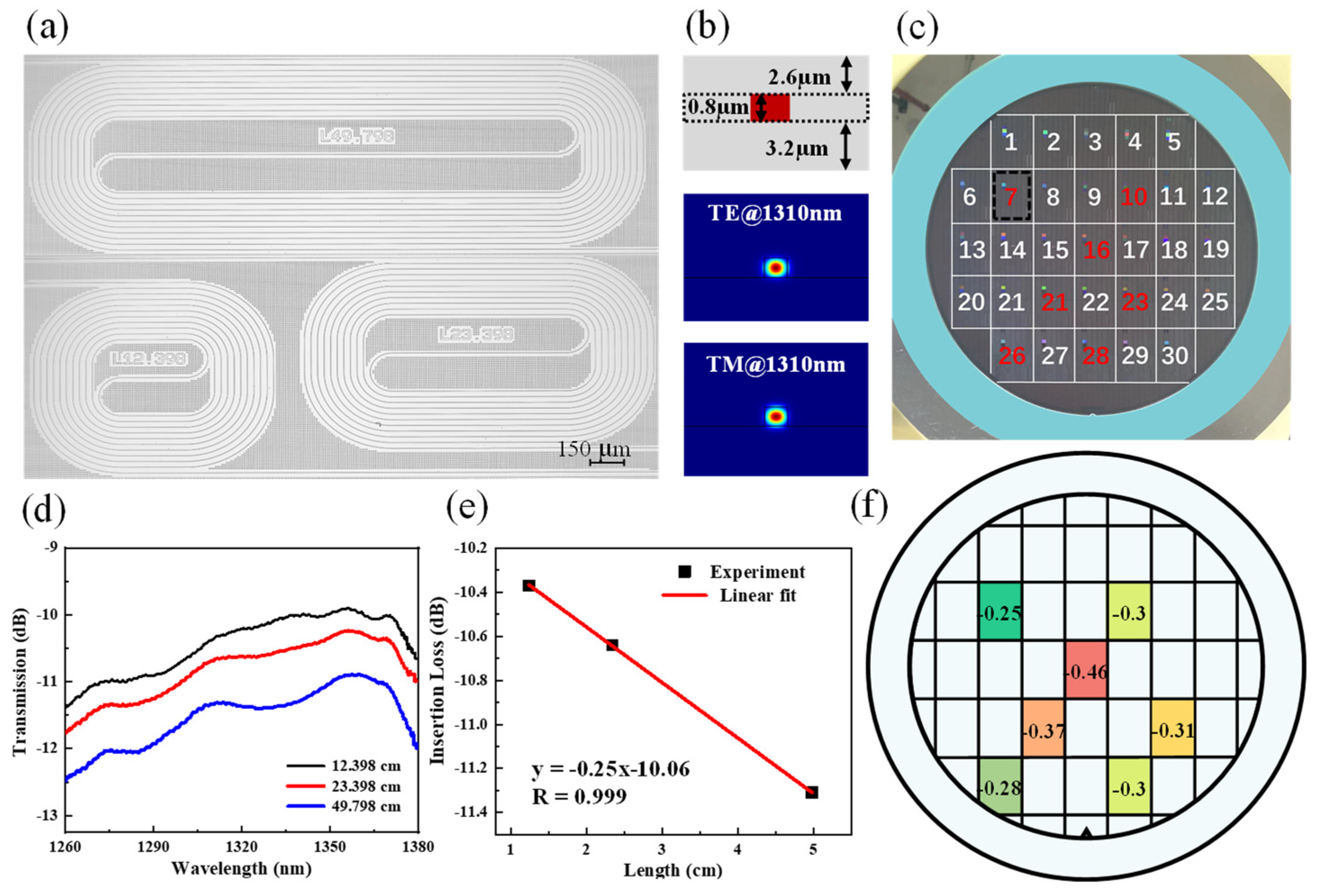
In silicon photonic integrated circuits, rectangular optical waveguides are the basic components. We have designed three sets of spiral waveguides with different lengths of 12.398, 23.398 and 49.798 mm; their optical photo is shown in
Figure 2a. The waveguide structure is shown in
Figure 2b (top), the thickness of the lower cladding layer is 3.2 µm and the thickness of the upper cladding layer is 2.6 µm. The thickness of the core layer is 0.8 µm and width of the waveguide is 0.8 µm. We have simulated the mode properties of the SiN waveguide using the Finite Difference Eigenmode solver (FDE) in Ansys Lumerical MODE. The mode field diagrams for the transverse electric (TE) and transverse magnetic (TM) modes at a wavelength of 1310 nm are depicted in the center and bottom of
Figure 2b, respectively. These diagrams clearly demonstrate that the waveguide dimensions effectively confine the light within its core. The photograph of the completed 8-inch wafer is displayed in
Figure 2c. The wafer comprises 30 individual dies, from which seven are highlighted in red for the purpose of propagation loss testing. The testing was conducted using a tunable laser that spans the O-band spectrum (model: Keysight 8164B). A lensed single-mode fiber was used to couple the light from the laser into the waveguide, and another lensed fiber was used to couple the light out of the waveguide to a power detector. The measured transmission spectra of spiral waveguides at Die 7 in the wavelength range of 1260 to 1380 nm is shown in
Figure 2d. We also measured the propagation loss by fitting the transmission spectrum of spiral waveguides of different lengths.
Figure 2e shows the results of the linear fit for the wavelength of 1310 nm, where the slope value obtained is −0.25, indicating that the propagation loss at 1310 nm is 0.25 dB/cm. A more comprehensive evaluation of device performance uniformity across the fabricated wafer is carried out by selecting spiral waveguides located in different dies.
Figure 2f presents the measured propagation losses at a wavelength of 1310 nm for the seven selected dies, the wafer level characteristics of the propagation losses of the waveguide are such that they gradually decrease from the center of the wafer to the edge of the wafer (red is the maximum loss, green is the minimum loss). The 800 nm thick SiN has better film uniformity and revealing an average loss that is less than 0.33 dB/cm.
4. 2 × 2 Multimode Interference (MMI) Coupler
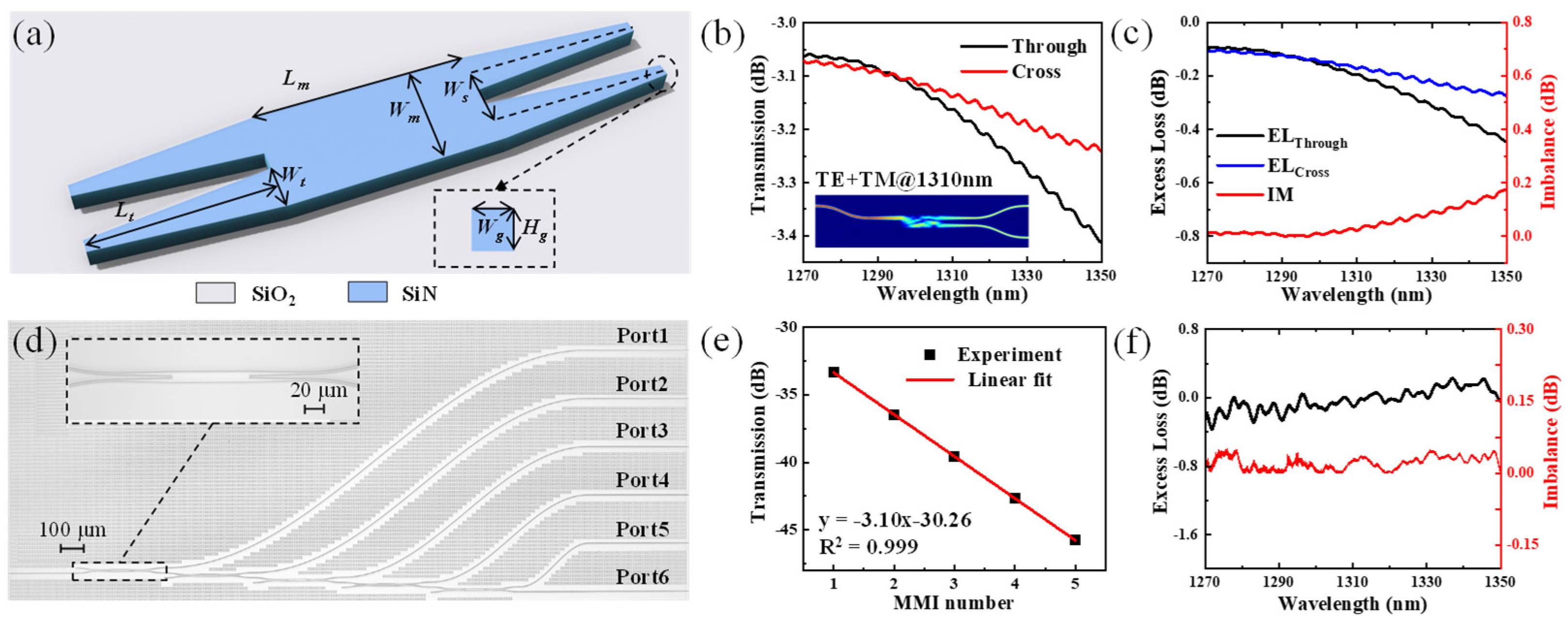
MMI is the most used on-chip power divider due to its wide manufacturing tolerance. As shown in
Figure 3a, we have designed and experimentally demonstrated a 2 × 2 SiN MMI 3-dB coupler. The designed 2 × 2 MMI 3-dB coupler was simulated by using the three-dimensional (3D) finite-difference time-domain (FDTD) method. Two orthogonal polarizations, TE and TM, combine to approximately represent the behavior of the Amplified Spontaneous Emission (ASE) light source to assess the response of beams of arbitrary polarization to the device. The multimode waveguide width
Wm is selected as 5.2 μm and the access port width
Wt of the linear taper to the multimode interference region is chosen to be 2 μm. The center-to-center spacing
Ws is set to 3.2 μm, providing ample separation to avoid crosstalk between the two input or output waveguides. The length of the taper
Lt is determined to be 55 μm, ensuring a sufficiently adiabatic transition within the tapers. Finally, the length of multimode waveguide
Lm is set to 79.3 μm in accordance with the beat length of the MMI coupler. Two inverse tapers with tip width of 300 nm and taper length of 300 μm are used to couple light in and out of the MMI coupler.
Both the through and cross ports of the coupler maintain a high transmittance over an 80-nm wide bandwidth from 1270 to 1350 nm in our simulation, as shown in
Figure 3b. The illustration shows the electric field distribution along the propagation. The imbalance (IM) is defined as
, the insertion loss (IL) of one output port is defined as
, and the excess loss (EL) is defined as the difference between the IL and the ideal −3 dB value for a 3-dB coupler are utilized to characterize the performance of the MMI coupler. In the definition,
PThrough,
PCross and
Pin represent the power at the through, cross and input ports, respectively. As shown in
Figure 3c, the simulation results illustrate that the MMI coupler exhibits relatively low
ELThrough (
ELCross) of below −0.44 (−0.27) dB and IM below 0.18 dB, respectively, across the entire 80-nm bandwidth.
To enable the most accurate calculation of the IL of a single MMI coupler, five identical MMIs are cascaded.
Figure 3d shows the optical microscope image of the fabricated MMIs tree, and the inset is an enlarged view of one single MMI coupler. Ports 1–6 are these output ports from each MMI coupler. In a fabricated MMI coupler tree, it can be observed that the power output from the ports decreases proportionally with an increasing number of cascaded MMI couplers. Consequently, the insertion loss of a single MMI can be determined by extracting the slope, which is calculated through linear fitting the power from the first five ports at each wavelength. We have measured the transmission spectra after calibrating to the light source across the wavelength regime of 1270–1350 nm.
Figure 3e presents the linear fitting results for the wavelength of 1310 nm, where the obtained slope is −3.10 dB, representing the IL of a single 2 × 2 MMI coupler. As a 3-dB coupler, the EL is calculated by subtracting the reference value of −3 dB, resulting in an EL of −0.10 dB at 1310 nm wavelength. The final two ports, Port 5 and Port 6, are used to calculate the IM of the coupler. Likewise, the EL and IM across the entire wavelength regime are calculated as shown in
Figure 3f. The measured EL is lower than −0.2 dB, and IM remains minimal, measuring less than 0.06 dB across the 80-nm bandwidth. Compared to the simulation results, which only consider the two orthogonal polarizations in the light source, the optimal test results may be caused by fabrication process errors of devices.
6. Optical Frequency Comb
Figure 5a is a schematic diagram of optical frequency comb generation. When the pump passes through a microcavity with non-linear characteristics and the phase matching requirement is met, the spectrum is broadened. The closer the integrated dispersion (
Dint) is to 0, the better the phase match between the microcavity mode and the comb mode at the corresponding wavelength, and the comb mode of the optical frequency comb can achieve more significant gain. If the slope of the
Dint curve is positive, the dispersion at the corresponding wavelength is anomalous dispersion; if the slope of the
Dint curve is negative, the dispersion at the corresponding wavelength is normal dispersion. The results show that it is easier to obtain anomalous dispersion with increasing silicon nitride thickness for the same waveguide width. As shown in
Figure 5b, a single frequency
ωp passes through the microcavity to produce optical frequencies
ωi and
ωs that are symmetric with the pump under the resulting generated four-wave mixing effect, their frequency spacing being
N1 times the FSR. Then, as the frequency combs expand under the non-generated four-wave mixing effect, any two frequencies
ω1 and
ω2 interact to produce new frequencies
ω3 and
ω4 separated by
N2 times the FSR. Finally, the two processes are performed simultaneously and the optical frequency comb is broadened.
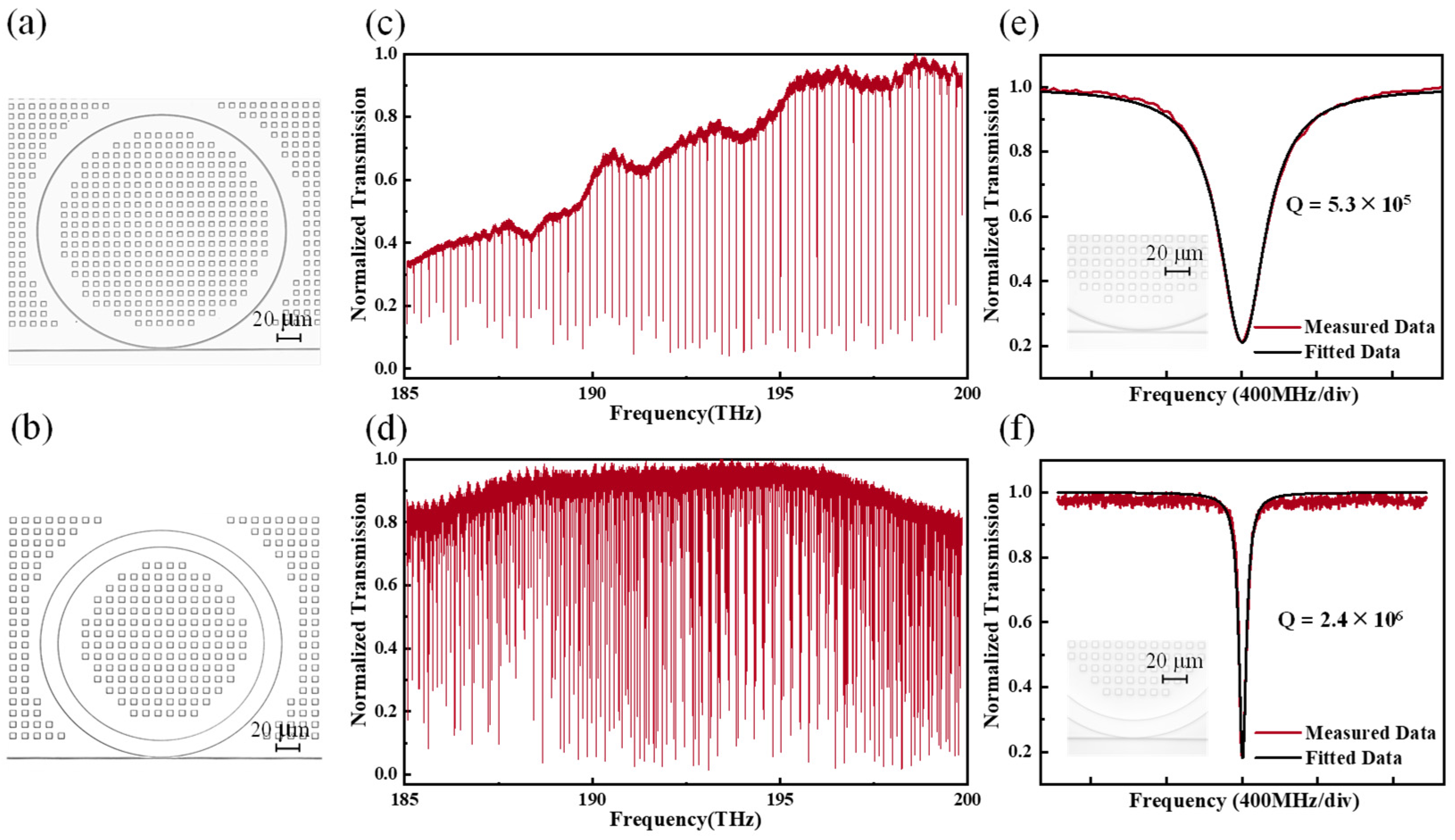
A broadband frequency comb is generated using a high-Q SiN resonator with anomalous GVD (GVD > 0). Low waveguide loss is often required for high Q. Dispersion control in micro-ring cavities is usually achieved by the width and height of the micro-ring cross section. In most silicon nitride microcavities, the thickness of the microcavity is very thin to achieve low transmission loss, resulting in dispersion that does not meet the requirements of nonlinear studies, especially those that produce optical free frequency combs. The key to thick silicon nitride microcavities is that the use of thick silicon nitride layers improves optical confinement, reduces scattering losses and allows to engineer dispersion. To meet the requirements of anomalous dispersion, the dimensions of the micro-ring usually allow the presence of multiple modes in the cavity, with a limited number of higher order modes in addition to the fundamental modes of TE and TM. We have selected specified resonance peaks from
Figure 4d and fitted the calculation to obtain the corresponding Q as shown in
Figure 5c. The width of 15 µm resonator has anomalous GVD and decent Q, micro-combs are expected to be generated in this resonator.
Before performing the comb generation experiments, we simulate the comb generation using the parameters of the 15 µm-wide resonator. The computational complexity of the coupled mode equations in the frequency domain increases with the number of comb teeth involved in the calculation. It is much easier to analyze the nonlinear dynamics of broadband microcavity optical frequency combs in the time domain, and the time-domain dynamics equations for microcavity combs are known as the Lutiato-Lefever equation (LLE). The following equation is the LLE, which is a nonlinear Schrödinger equation with dissipation and pumping terms. The use of the LLE allows for rapid simulation and analysis of the evolution of the optical frequency combs.
For a microcavity, its internal optical field can be described as a function of spatial position and time . The resonance frequency of the pump mode is , and since the micro-optical comb usually extends on both sides of the frequency domain with the pump light as the center, the relative mode number is introduced, and the relative mode number of the pump mode is 0. denotes the amount of detuning of the pump with respect to the resonance frequency of the pump mode and the single-photon energy , is the total loss of the combs and is the coupling loss of the microcavities, is the optical power of the pump. The equivalent non-linear coefficient (where is the equivalent non-linear coefficient, is the refractive index of the material and is the effective mode volume of the mode field).
To optimize the characterization process of the micro-optic comb, we employ Python 3.11.5 scripts to calculate the LLE for each parameter of the 15 µm-wide resonator. The evolution of the total intracavity power in the simulation is depicted in
Figure 5d. The analysis reveals that as the pump laser frequency is scanned from the blue-detuned side towards the red-detuned side of the pump mode, there is a gradual increase in the intracavity power. A critical point is observed in
Figure 5e, where the intracavity power surpasses the nonlinear threshold. Beyond this threshold, the main comb emerges with a spacing many times the FSR of the micro-ring resonator.
The experimental setup for comb generation consists of laser generation and amplification, a micro-ring resonator chip and electronics for monitoring various parameters. Laser generation and amplification are facilitated by a tunable laser (Toptica CTL1550) and an Erbium-Doped Fiber Amplifier (EDFA), with the latter providing amplification across the optical spectrum of approximately 1550–1570 nm, aligning with the pump light’s tuning range. The pump light’s polarization is fine-tuned using a fiber polarization controller (FPC) to ensure optimal alignment with the micro-ring’s mode. The laser is coupled to the micro-ring chip through a lensed optical fiber. In our experiments, the formation of the main comb was observed by applying pump power of 500 mW at a pump wavelength of 1559 nm, as illustrated in
Figure 5f. Probably due to the mismatch between the corresponding mode and the pumping power, only the main comb was achieved, which agreed with the simulation as shown in
Figure 5e. While, soliton generation was not observed, primarily due to the multitude of modes in the micro-ring and their polarization-sensitive resonance peaks. To induce soliton formation, further experiments with iterative polarization adjustments to identify the requisite stepped resonance peaks are required.

 ,
, 


