Article

A Multi-Parameter Tunable and Compact Plasmon Modulator in the Near-Infrared Spectrum

1
College of Digital Technology and Engineering, Ningbo University of Finance & Economics, Ningbo 315175, China
2
Ningbo Yongxin Optics Co., Ltd., Ningbo 315040, China
3
Ningbo Institute of Education Sciences, Ningbo 315099, China
4
Advanced Photonics Center, School of Electronic Science & Engineering, Southeast University, Nanjing 210018, China
5
School of Information Technology, Jiangsu Open University, Nanjing 210036, China
*
Author to whom correspondence should be addressed.
Photonics 2024, 11(6), 530; https://doi.org/10.3390/photonics11060530
Submission received: 25 April 2024 / Revised: 27 May 2024 / Accepted: 29 May 2024 / Published: 3 June 2024
(This article belongs to the Special Issue Advancements in Optical Sensing and Communication Technologies)

Abstract

:
To keep pace with the demands of modern photonic integration technology, the electro-optic modulator should feature multi-parameter tunable components and a compact size. Here, we propose a hybrid structure that can modulate the multi-parameters of surface plasmon polaritons (SPPs) simultaneously with a compact size by controlling the electron concentration of indium tin oxide (ITO) in the near-infrared spectrum. The length, width and height of the device are only 15 μm, 5 μm and 9 μm, respectively. The numerical results show that when the electron concentration in ITO changes from 7.5 × 1026 m−3 to 9.5 × 1026 m−3, the variation in amplitude, wavelength and phase are 49%, 300 nm and 347°, respectively. The demonstrated structure paves a new way for multi-parameter modulation and the realization of ultracompact modulators.

1. Introduction

Manipulating the fundamental characteristics of light, including polarization, wavelength, amplitude and phase, is crucial in modern photonic integration technology [1,2,3,4]. The ability to simultaneously control these properties is of great significance and has promising applications in areas such as modulators, sensors and photodetectors [5,6,7,8]. For instance, in quadrature amplitude modulation (QAM) schemes, the precise adjustment of signal amplitude and phase is necessary to generate a constellation of points, each corresponding to a unique combination of amplitude and phase [9]. In numerous beam-forming networks, tailored amplitude and phase settings are utilized to activate the individual components of the network [10].
Recently, numerous research has been conducted in the field of multi-parameter modulation to address the growing needs of diverse applications [11,12,13]. For example, Mohamad’s team has developed four innovative and easy-to-fabricate structures for the creation of high-performance polarization-insensitive modulators that can control both amplitude and phase [14]. Ali Forouzmand’s team has put forward an electrically tunable amplitude and phase modulator, in which the indium tin oxide (ITO) is incorporated into a guided-mode resonance mirror [15]. Nonetheless, despite their advanced merits, these proposed modulators are limited to controlling one or two parameters of light, which significantly impedes their broader application. Our group has reported a plasmon modulator that can control the amplitude, wavelength and phase simultaneously based on a hybrid silicon-dielectric-graphene structure, but it has limited application scenarios as a result of the restricted working wavelength of graphene plasmon [16]. With the development of modern semiconductor materials and photoelectric integration technology, semiconductors are playing an important role in the field of modern communication systems and integrated circuits [17,18]. The multi-parameter modulation in semiconductors has broad application prospects in fields such as semiconductor chips, lighting equipment and optical storage [19,20,21,22]. Thus, it is highly desirable to develop a new method that aims to realize multi-parameter modulation in semiconductors which mainly works in the near-infrared spectrum. Compared with other plasmonic materials in this band, the ITO presents good metal-like optical properties and can be heavily doped. What is more, its electron concentration can be easily modulated by the applied voltage. Herein, the ITO is selected as the alternative material for the plasmon modulator [23].
In this work, a hybrid structure, which can modulate multi-parameters of surface plasmon polaritons (SPPs) simultaneously with a compact footprint by controlling the electron concentration of ITO in the near-infrared spectrum, is proposed and designed. The numerical results show that when the electron concentration in ITO changes from 7.5 × 1026 m−3 to 9.5 × 1026 m−3, the variation in amplitude, wavelength and phase are 49%, 300 nm and 347°, respectively. This scheme paves a new way for multi-parameter modulation and the realization of ultracompact modulators.

2. Model and Simulation

The three-dimensional (3D) schematic diagram of our proposed structure is depicted in Figure 1. The length, width and height of the device are only 15 μm, 5 μm and 9 μm, respectively. A transverse magnetic (TM) polarized light incidents on the ITO grating, thereby inducing the SPPs to propagate along the surface of the ITO. (The ITO grating is only utilized to compensate for the wave vector mismatch and excite the SPPs because this way has a good excitation efficiency to the SPPs.) The ITO acts as the propagating layer of SPPs. The electron is close to or far away from the surface when the voltage is applied between two silicon substrates. Herein, the electron concentration of ITO can be controlled and yield an obvious change in the refractive index of ITO, and this strong nonlinear effect can improve the modulation performance effectively [24,25,26] so that the amplitude, wavelength and phase of the SPPs are modulated simultaneously as these parameters strongly depend on the refractive index of ITO. Calcium fluoride (CaF2) demonstrates superior qualities, including minimal leakage current, strong dielectric strength and a low defect count. Consequently, we have chosen CaF2 to serve as the dielectric layer, which can significantly enhance the performance of the modulator.
The conceptualized structure is modeled using the finite element method (FEM), and the two-dimensional (2D) simulation model is displayed in Figure 2. The port mode is employed to stimulate the surface plasmon polaritons (SPPs). (Given that the role of the grating is solely to excite the SPPs, it is deemed superfluous to include the grating in the simulation as other excitation techniques can also be utilized in this model.) Subsequently, the characteristics of SPPs are examined by varying the electron concentration in ITO. Initially, the electric field distribution and optical transmission are utilized to exhibit the modulation of the amplitude. Then, the alteration of wavelength can be discerned from the distribution of the electric field too. Lastly, the phase distribution within this model also indicates the propagating properties of SPPs. Hence, the amplitude, wavelength and phase of the SPPs can be clearly reflected by the designed simulation model.
The dielectric constant is used in the simulation process, and the relationship between plasmon frequency and the dielectric constant can be obtained from Equation (1) [27]:
ε = ε ω p 2 ω 2 + i ω Γ
where ε is the high-frequency dielectric constant, ω is the angular frequency, ωp is the plasma frequency and Γ is the relaxation frequency. The relationship between plasmon frequency and electron concentration is shown in Equation (2):
ω p 2 = N e 2 ε 0 m *
where N is the electron concentration, e is the electron charge, ε0 = 8.85 × 10⁻¹² Fm−1 is the dielectric constant in the vacuum, m* = 0.35 m0 is the electron effective mass and m0 = 9.1 × 10⁻³¹ kg is the mass of electrons. The relationship between the dielectric constant and the electron concentration can be obtained by combining Equation (1) with (2), and the corresponding real part (n) and the imaginary part (k) of effective refractive index at different electron concentrations can also be calculated. The real part and imaginary part of the ITO refractive index versus the electron concentration are shown in Figure 3a and Figure 3b, respectively, when the wavelength is fixed at 1.55 μm, which can be utilized in the proposed simulation model.

3. Results and Discussion

3.1. Modulation in Propagating Distance

Figure 4 illustrates the y component of the electric field at various electron concentrations with the working wavelength fixed at 1.55 μm. Figure 4a displays the y-component distribution of the electric field at an electron concentration of 7.5 × 1026 m−3, exhibiting a typical attenuation characteristic of SPPs. Figure 4b presents the y-component distribution of the electric field when the electron concentration is raised to 8.5 × 1026 m−3 by increasing the applied voltage. It can be obtained that the SPPs can propagate a longer distance compared with Figure 4a because the propagating SPPs are better localized as the electron concentration increases and the metallic characteristics become more obvious. With the electron concentration continuing to increase to 9.5 × 1026 m−3, the y-component distribution of the electric field is shown in Figure 4c. It can be clearly seen that the propagating distance of SPPs becomes longer, which demonstrates that the proposed model can modulate the propagating distance of SPPs effectively, and the propagating distance changed by 2.7 μm. (The propagating distance is 2.08 μm when the electron concentration is 7.5 × 1026 m−3, while the propagating distance is increased to 4.78 μm when the electron concentration is 9.5 × 1026 m−3.)

3.2. Modulation in Amplitude

Figure 5 illustrates the correlation between the electric field intensity and the electron concentrations. It is observable that the intensity of the second peak in the electric field increases from 1.63 × 10⁴ V/m to 2.10 × 10⁴ V/m as the electron concentration rises from 7.5 × 1026 m−3 to 8.5 × 1026 m−3. The electric field strength even reached 2.43 × 10⁴ V/m when the electron concentration sustainably increased to 9.5 × 1026 m−3, and the electric intensity changed by 49%. It can be demonstrated that the amplitude of SPPs gradually enhances as the electron concentration increases owing to the ITO being of a stronger metallicity leading to the propagating SPPs being localized better and transported a longer distance. Herein, the amplitude of the SPPs is modulated by the proposed model.

3.3. Modulation in Optical Transmission

Figure 6 demonstrates the relationship between optical transmission and electron concentrations. There is a noticeable enhancement in optical transmission thanks to the reduction in propagation losses when the electron concentration increases. This underscores that our model is capable of modulating the amplitude of the propagating SPPs efficiently by adjusting the electron concentration in ITO. The optical transmission is −75.2 dB (−22.2 dB) when the electron concentration is 7.5 × 1026 m−3 (9.5 × 1026 m−3). The optical transmission changes by 53 dB.

3.4. Modulation in Wavelength

Figure 7 depicts the relationship between the wavelength of SPPs and the electron concentration in ITO. It is evident that the wavelength of the SPPs in propagation increases as the electron concentration rises, due to the wavelength of SPPs in ITO being positively correlated with the electron concentration of ITO [28,29]. The wavelength is changed by 300 nm when the electron concentration of ITO increases from 7.5 × 1026 m−3 to 9.5 × 1026 m−3 (1360 nm at 7.5 × 1026 m−3 while 1660 nm at 9.5 × 1026 m−3). These findings confirm that the wavelength of the SPPs can be effectively modulated by the proposed structure.

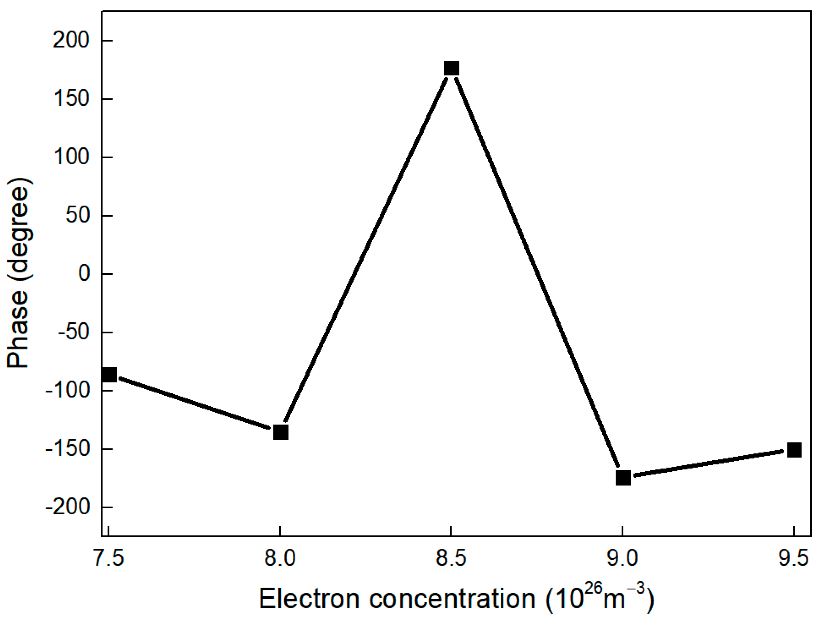
3.5. Modulation in Phase

Figure 8 illustrates the x component of the phase distribution when the electron concentrations of ITO are 7.5 × 1026 m−3, 8.5 × 1026 m−3 and 9.5 × 1026 m−3, respectively. It is distinctly observable that the phase exhibits varied distributions at different electron concentrations, thereby confirming that our proposed structure can also control the phase of SPPs dynamically. The reason why the phase can be modulated is that the modulation in electron concentration leads to a change in the refractive index of ITO, and the phase of propagating SPPs is strongly associated with the refractive index of ITO as the optical path is changed.
Figure 9 illustrates the relationship between the phase at the right port and the electron concentrations. The phase angle is 177° at an electron concentration of 8.5 × 1026 m−3. Conversely, the phase angle is −170° at an electron concentration of 9.0 × 1026 m−3, resulting in a phase variation of 347°. This phenomenon occurs because the phase of the propagating SPPs is influenced by the refractive index that is modulated by the electron concentration in ITO.

4. Conclusions

In conclusion, we have engineered and presented a hybrid silicon-dielectric-ITO configuration, and it can modulate the amplitude, wavelength and phase of SPPs simultaneously with a compact size by manipulating the electron concentration in ITO. The numerical results indicate that a change in the electron concentration of ITO from 7.5 × 1026 m−3 to 9.5 × 1026 m−3 leads to respective modulations of 49% in amplitude, 300 nm in wavelength, and 347° in phase. The capability to achieve multi-parameter modulation of SPPs with a compact size holds great potential for applications in optical communications, sensing and photodetection technologies.

Author Contributions

Conceptualization, X.H.; methodology, C.L.; software, X.Z.; data curation, M.L.; writing—original draft preparation, S.Y.; writing—review and editing, H.W. All authors have read and agreed to the published version of the manuscript.

Funding

The work was financially supported by the National Natural Science Foundation of China (NSFC) (12274075) and the Scientific Research Fund of Zhejiang Provincial Education Department (Y202352891).

Data Availability Statement

The data relative to the experiments discussed in this work are available upon reasonable request from the corresponding author Xuefang Hu.

Conflicts of Interest

Authors Xuefang Hu and Hongfei Wan were employed by the company Ningbo Yongxin Optics Co., Ltd. The remaining authors declare that the research was conducted in the absence of any commercial or financial relationships that could be construed as a potential conflict of interest.

References

  1. Liu, M.; Yin, X.; Ulin-Avila, E.; Geng, B.; Zentgraf, T.; Ju, L.; Wang, F.; Zhang, X. A graphene-based broadband optical modulator. Nature 2011, 474, 64–67. [Google Scholar] [CrossRef]
  2. Melikyan, A.; Alloatti, L.; Muslija, A.; Hillerkuss, D.; Schindler, P.C.; Li, J.; Palmer, R.; Korn, D.; Muehlbrandt, S.; van Thourhout, D.; et al. High-speed plasmonic phase modulators. Nat. Photonics 2014, 8, 229–233. [Google Scholar] [CrossRef]
  3. Wei, H.; Wang, Z.; Tian, X.; Käll, M.; Xu, H. Cascaded logic gates in nanophotonic plasmon network. Nat. Commun. 2011, 2, 387. [Google Scholar] [CrossRef]
  4. Zhu, L.; Fan, Y.; Wu, S.; Yu, L.; Zhang, K.; Zhang, Y. Electrical control of terahertz polarization by graphene microstructure. Opt. Commun. 2015, 346, 120–123. [Google Scholar] [CrossRef]
  5. Thijssen, R.; Verhagen, E.; Kippenberg, T.J.; Polman, A. A Plasmon nanomechanical coupling for nanoscale transduction. Nano Lett. 2013, 13, 3293–3297. [Google Scholar] [CrossRef]
  6. Schuller, J.A.; Barnard, E.S.; Cai, W.; Jun, Y.C.; White, J.S.; Brongersma, M.L. Plasmonics for extreme light concentration and manipulation. Nat. Mater. 2010, 9, 193–204. [Google Scholar] [CrossRef]
  7. Sorger, V.J.; Ye, Z.; Oulton, R.F.; Wang, Y.; Bartal, G.; Yin, X.; Zhang, X. Experimental demonstration of low-loss optical waveguiding at deep sub-wavelength scales. Nat. Commun. 2011, 2, 331. [Google Scholar] [CrossRef]
  8. Ozbay, E. Plasmonics: Merging photonics and electronics at nanoscale dimensions. Science 2006, 311, 189–193. [Google Scholar] [CrossRef]
  9. Correia, R.; Boaventura, A.; Carvalho, N.B. Quadrature amplitude backscatter modulator for passive wireless sensors in IoT applications. IEEE Trans. Microw. Theory Tech. 2017, 65, 1103–1110. [Google Scholar] [CrossRef]
  10. Moon, S.-M.; Yun, S.; Yom, I.-B.; Lee, H.L. Phased array shaped-beam satellite antenna with boosted-beam control. IEEE Trans. Antennas Propag. 2019, 67, 7633–7636. [Google Scholar] [CrossRef]
  11. Han, S.; Kim, S.; Kim, S.; Low, T.; Brar, V.W.; Jang, M.S. Complete complex amplitude modulation with electronically tunable graphene plasmonic metamolecules. ACS Nano 2020, 14, 1166–1175. [Google Scholar] [CrossRef]
  12. Su, D.; Wang, X.; Shang, G.; Ding, X.; Burokur, S.N.; Liu, J.; Li, H. Amplitude-phase modulation metasurface hologram with inverse angular spectrum diffraction theory. J. Phys. D Appl. Phys. 2022, 55, 235102. [Google Scholar] [CrossRef]
  13. Ren, Z.; Xu, J.; Liu, J.; Li, B.; Zhou, C.; Sheng, Z. Active and Smart Terahertz Electro-Optic Modulator Based on VO2 Structure. ACS Appl. Mater. Interfaces 2022, 14, 26923–26930. [Google Scholar] [CrossRef]
  14. Najafi Hajivar, M.; Hosseini-Farzad, M. Buried and ridge graphene-based silicon waveguides for broadband polarization-insensitive amplitude and phase modulators. arXiv 2019, arXiv:1912.06801. [Google Scholar] [CrossRef]
  15. Forouzmand, A.; Mosallaei, H. Electro-optical amplitude and phase modulators based on tunable guided-mode resonance effect. ACS Photonics 2019, 6, 2860–2869. [Google Scholar] [CrossRef]
  16. Hu, X.; Lu, C.; Zhao, X.; Gu, Y.; Lu, M.; Sun, D. A multi-parameter tunable plasmon modulator. Sci. Rep. 2023, 13, 11483. [Google Scholar] [CrossRef]
  17. Wang, B.; Blaize, S.; Seok, J.; Kim, S.; Yang, H.; Salas-Montiel, R. Plasmonic-Based Subwavelength Graphene-on-hBN Modulator on Silicon Photonics. IEEE J. Sel. Top. Quantum Electron. 2019, 25, 1–6. [Google Scholar] [CrossRef]
  18. Vinnakota, R.K.; Genov, D.A. Active Control of Charge Density Waves at Degenerate Semiconductor Interfaces. Sci. Rep. 2017, 7, 10778. [Google Scholar] [CrossRef]
  19. Le, K.Q. ITO-based Electro-Optical Modulator Integrated in Silicon-On-Insulator Waveguide Using Surface Plasmon Interference. Phys. B Condens. Matter 2021, 602, 412313. [Google Scholar] [CrossRef]
  20. Zhu, S.; Yu, Z.; Liu, L.; Yang, C.; Cao, H.; Xi, X.; Li, J.; Zhao, L. Enhancing the spontaneous emission rate by modulating carrier distribution in GaN-based surface plasmon light-emitting diodes. Opt. Express 2017, 25, 9617–9627. [Google Scholar] [CrossRef]
  21. Kelley, M.; Lee, A.; Mozumdar, M.; Dajani, K.; Ahmed, A. Design and modeling of subpicosecond all-optical modulator using the nonlinear response of indium tin oxide. J. Opt. Soc. Am. B 2019, 36, F149–F153. [Google Scholar] [CrossRef]
  22. Xu, X.; Chen, W.; Zhang, S.; Liu, C.; Sun, R.; Li, Z.; Zhang, B. Numerical Analysis for a P-Drift Region N-IGBT With Enhanced Dynamic Electric Field Modulation Effect. IEEE Trans. Electron. Devices 2022, 69, 3277–3282. [Google Scholar] [CrossRef]
  23. Naik, G.V.; Shalaev, V.M.; Boltasseva, A. Alternative plasmonic materials: Beyond gold and silver. Adv. Mater. 2013, 25, 3264–3294. [Google Scholar] [CrossRef] [PubMed]
  24. Li, W.; Liu, Y.; Ling, L.; Sheng, Z.; Cheng, S.; Yi, Z.; Wu, P.; Zeng, Q.; Tang, B.; Ahmad, S. The tunable absorber films of grating structure of AlCuFe quasicrystal with high Q and refractive index sensitivity. Surf. Interfaces 2024, 48, 104248. [Google Scholar] [CrossRef]
  25. Liang, S.; Xu, F.; Li, W.; Yang, W.; Cheng, S.; Yang, H.; Chen, J.; Yi, Z.; Jiang, P. Tunable smart mid infrared thermal control emitter based on phase change material VO2 thin film. Appl. Therm. Eng. 2023, 232, 121074. [Google Scholar] [CrossRef]
  26. Carrillo-Delgado, C.; Arano-Martínez, J.A.; Vidales-Hurtado, M.A.; Torres-Torres, D.; Martínez-González, C.L.; Torres-Torres, C. Electrically induced directional self-focusing in electrochromic NiO thin solid films. J. Mater. Sci. Mater. Electron. 2023, 34, 953. [Google Scholar] [CrossRef]
  27. Feigenbaum, E.; Diest, K.; Atwater, H.A. Unity-Order Index Change in Transparent Conducting Oxides at Visible Frequencies. Nano Lett. 2010, 10, 2111–2116. [Google Scholar] [CrossRef] [PubMed]
  28. Lu, H.; Wang, R.; Bao, F.; Ye, J.; Lin, H.; Zhu, H.; Wan, M.; Yang, H.; Shen, K.; Mai, Y. Preparation and investigation of ITO/metal/ITO electrodes for electrochromic application. Opt. Mater. 2022, 133, 112848. [Google Scholar] [CrossRef]
  29. Lee, G.; Park, E.; Nguyen, V.T.; Heo, S.; Nguyen, N.A.; Larina, L.L.; Yoon, I.; Choi, H.S. Plasma-assisted ITO sol coating for optimizing the optoelectronic properties of ITO glass. Appl. Surf. Sci. 2021, 551, 149414. [Google Scholar] [CrossRef]
Figure 1. Three-dimensional schematic diagram of multi-parameter joint control modulator.
Photonics 11 00530 g001
Figure 2. Two-dimensional simulation diagram of multi-parameter tunable modulator.
Photonics 11 00530 g002
Figure 3. (a) The real part of the ITO refractive index (n) and (b) the imaginary part of the refractive index (k) versus different electron concentrations.
Photonics 11 00530 g003
Figure 4. Distribution of y component of electric field intensity with its electron concentration at (a) 7.5, (b) 8.5, and (c) 9.5 × 1026 m−3.
Photonics 11 00530 g004aPhotonics 11 00530 g004b
Figure 5. Distribution of electric intensity versus different electron concentrations.
Photonics 11 00530 g005
Figure 6. The relationship between optical transmission and the electron concentration of ITO.
Photonics 11 00530 g006
Figure 7. The relationship between the wavelengths of SPPs and electron concentrations.
Photonics 11 00530 g007
Figure 8. X component of phase distribution under different electron concentrations: (a) 7.5 and (b) 8.5 (c) 9.5 × 1026 m−3.
Photonics 11 00530 g008aPhotonics 11 00530 g008b
Figure 9. Phase change diagram under different electron concentrations.
Photonics 11 00530 g009
Disclaimer/Publisher’s Note: The statements, opinions and data contained in all publications are solely those of the individual author(s) and contributor(s) and not of MDPI and/or the editor(s). MDPI and/or the editor(s) disclaim responsibility for any injury to people or property resulting from any ideas, methods, instructions or products referred to in the content.

