Review

Increase in Modulation Speed of Silicon Photonics Modulator with Quantum-Well Slab Wings: New Insights from a Numerical Study

Department of Electrical and Electronic Engineering, School of Engineering, Tokyo Institute of Technology, 2-12-1, Ookayama, Meguro-Ku, Tokyo 152-8550, Japan
Photonics 2024, 11(6), 535; https://doi.org/10.3390/photonics11060535
Submission received: 8 May 2024 / Revised: 30 May 2024 / Accepted: 31 May 2024 / Published: 3 June 2024
(This article belongs to the Special Issue Novel Advances in Integrated Optics)

Abstract

:
A Silicon Photonics modulator is a high-speed photonic integrated circuit for optical data transmission in high-capacity optical networks. Silicon Photonics modulators in the configuration of a Mach–Zehnder interferometer, in which a PN-junction rib-waveguide phase shifter is inserted in each arm of the interferometer, are studied in this paper because of their superior performance of high-quality optical data generation in a wide range of spectral bands and their simplicity in fabrication processes suitable to production in foundries. Design, fabrication, and fundamental characteristics of Silicon Photonics Mach–Zehnder modulators are reviewed as an introduction to these high-speed PICs on the Silicon Photonics platform. Modulation speed, or modulation bandwidth, is a key performance item, as well as optical loss, in the application to high-speed optical transmitters. Limiting factors on modulation speed are addressed in equations. Electrical resistance–capacitance coupling, which causes optical modulation bandwidth–optical loss trade-off, is the most challenging limiting factor that limits high-speed modulation. Expansion of modulation bandwidth is not possible without increasing optical loss in the conventional approaches. A new idea including quantum-mechanical effect in the design of Silicon Photonics modulators is proposed and proved in computational analysis to resolve the bandwidth loss trade-off. By adding high-mobility quantum-well overlayers to the side slab wings of the rib-waveguide phase shifter, the modulation bandwidth is doubled without increasing optical loss to achieve a 200 Gbaud modulation rate.

1. Introduction

High-speed carrier-depletion optical modulators designed and fabricated on complementary metal–oxide–semiconductor (CMOS)-based integrated-photonics platforms are photonic integrated circuits that have small footprints and are fabricated in low-cost processes [1,2,3,4]. Silicon Photonics modulators have now been available from commercialized Silicon Photonics foundries and extensively applied to modern optical networks of high transmission capacity [5,6,7,8]. Further enhancement of modulation speed, namely the expansion of modulation bandwidth, is required for the Silicon Photonics modulators to realize higher transmission capacity without a significant increase in optical loss. Reverse-biased PN-junction phase shifters are the key parts of high-speed Silicon Photonics modulators; therefore, an increase in modulation bandwidth in the PN-junction phase shifters is crucial in the advances in modern optical networks [9].
In this paper, an idea is proposed and verified in numerical analysis to realize the significant expansion of modulation bandwidth of the Silicon Photonics modulators without increasing optical loss. Before elaborating on the idea, the current carrier-depletion Silicon Photonics modulators are first reviewed in the aspects of design, fabrication, and performance. Physical factors limiting the modulation bandwidth of reverse-biased PN-junction phase shifter are clarified based on electronic–photonic simulation characteristics on phase-shifter responses and experimental characteristics on optical modulation bandwidth and transient waveform. It is shown that the resistance–capacitance (RC) coupling in the phase shifters is the most dominant factor, with which the optical bandwidth–loss trade-off arises [10,11]. For bandwidth enhancement, a reduction in electrical series resistance without decreasing the electrical capacitance of the PN junction is required because the lower junction capacitance leads to poorer modulation efficiency. The conventional way to reduce the series resistance is to increase the carrier concentration with P- and N-type doping. Optical loss due to free-carrier absorption is higher, however, if the doping concentration is increased [11]. The higher optical loss implies that higher optical power input to the optical networks is necessary to maintain high transmission performance. The increase in optical power is not suitable for modern optical networks as ecosystems.
An approach to the reduction in the series resistance without causing the increase in optical loss is proposed in this paper to resolve the optical bandwidth–loss trade-off. The essential part of the approach is to introduce high-mobility two-dimensional (2D) carriers to the side slabs of the rib-waveguide phase shifter on the Silicon Photonics platform. Heterojunction consisting of undoped SiGe thin film on Si, that forms a quantum well (QW), allows high-mobility transport of 2D carriers confined in the QW. The carriers, which are confined in the QW by selective doping in the Si slab layer, do not suffer from mobility reduction due to scattering at ionized impurity centers because the carriers in the QW are separated from the ionized impurities in the Si slab layer. Such a mobility-enhancement mechanism was applied to the high-mobility heterojunction transistors [12,13,14,15,16]. Based on this mechanism, resistance reduction without increasing dopant concentration can be achieved in the phase shifter.
Reverse-biased PN-junction rib-waveguide phase-shifter integrated with high-mobility SiGe/Si QW slab wings is modeled and analyzed in electronic–photonic simulation. The simulation method includes solving carrier profiles using classical technology computer-aided design (TCAD) plus the numerical solution of the one-dimensional (1D) Schrödinger equation and simultaneously obtaining the mode profiles from an optical guided-mode solver. Numerical results on optical modulation bandwidth and optical loss of the phase shifter integrated with the QWs are presented and compared with those of the current Silicon Photonics phase shifter without the QWs. Low-loss optical modulation beyond 100 Gbaud is predicted for the phase shifter, which can be accommodated in CMOS design and fabrication platforms in Silicon Photonics foundries.

2. Review of Carrier-Depletion Silicon Photonics Modulators

Carrier-depletion Silicon Photonics modulators are photonic integrated circuits (PICs) designed and fabricated on a CMOS-based platform. Basic design, modulator performance, and limiting factors on modulation speed are presented in this section.

2.1. Design Considerations

The waveguide geometry of the Mach–Zehnder (MZ) interferometer has been used extensively as the basic layout of integrated Silicon Photonics modulators, which generate high-speed optical data in a variety of modulation formats in broad spectral ranges extending over C and O bands. An integrated Silicon Photonics modulator chip for operation in advanced modulation formats such as 256 Gb/s 32 Gbaud 16 QAM (Quadrature Amplitude Modulation) is shown in Figure 1 [9,17]. The integrated Silicon Photonics modulator consists of dual in-phase–quadrature (IQ) modulator blocks for the generation of optical data in two-orthogonal polarization modes, X and Y. Each of the dual IQ modulator blocks is constructed in the layout of nested MZ interferometer, in which a sub-MZ modulator interferometer is inserted to each phase-shifter arm of the main nested MZ interferometer. A sub-MZ modulator block is driven in push–pull mode for zero frequency chirp to avoid optical data distortion [18,19,20]. In the push–pull mode, electrical data in opposite signs are complementarily applied to dual phase-shifter arms in the sub-MZ modulator block, respectively. The integrated high-speed modulator was designed and fabricated in collaboration with the Institute of Microelectronics, Singapore [20].
In 256 Gb/s 16 QAM, 128 Gb/s 16 QAM optical data are generated in each IQ modulator block in the fundamental mode of transverse-electric (TE) polarization. The polarization of the waveguide mode from one of the IQ modulator blocks, for instance, YIQ, is then converted to transverse-magnetic (TM) mode, in which the electric field of the mode is rotated 90 deg from the TE mode in a polarization-division multiplexer (PDM) and multiplexed with the optical data in the TE mode from the other IQ modulator part, XIQ. All the waveguide blocks for the PDM IQ modulator were integrated into a PIC chip with a footprint as small as 6 × 5 mm2.
The optical waveguides constituting Silicon Photonics MZ modulators are rib and channel waveguides. Cross-sections of the optical waveguides are illustrated in Figure 1c. A rib waveguide of 500 nm rib width and 220 nm height is inserted in each arm of the MZ interferometer as a phase shifter. In the rib waveguide, a PN junction is formed and reverse bias is applied to the PN junction to modulate the optical phase based on free-carrier plasma refraction. The optical waveguides connected to the rib-waveguide phase shifters are channel waveguides of 500 nm width and 220 nm height. Typically, the width is chosen between 450 and 500 nm for the rib and channel waveguides. To form a beam splitter and beam combiner of an MZ interferometer, a 1 × 2 multi-mode interferometer has been used for Silicon Photonics modulators [9].
The phase shifter is the most crucial part of the MZ modulator. A type of PN-junction rib-waveguide phase shifter in the Silicon Photonics modulators is visualized in its cross-section in Figure 2. An “L”-shaped PN junction was formed in the phase shifter to achieve high modulation efficiency, namely low π-shift voltage, Vπ. The designed PN-junction profile was transferred well in the fabricated phase shifters, as confirmed in the scanning capacitance microscopy (SCM) profile [17]. The dimension of the fabricated rib waveguide of the phase shifter coincides almost perfectly with the designed specifications of 220 nm height at the center and 100 nm height at the side slabs, as evidenced in the cross-section image of the phase shifter in the transmission electron microscopy (TEM) photograph.

2.2. Fabrication Processes

The wafers of the Silicon Photonics modulators have been fabricated in CMOS-based fabrication lines using silicon-on-insulator (SOI) wafers in 200 or 300 mm diameter. A thin SOI layer of 220 nm thickness has been used extensively to form a single-mode optical waveguide core made of crystalline silicon for passive and active blocks of the modulators with the cross-sections, as illustrated in Figure 3 [9]. The active blocks are the rib-waveguide phase shifters and Ge photodetectors (PDs) in the case of the Silicon Photonics modulator integrated with Ge PDs for monitoring and conditioning of modulation performance. The buried oxide (BOX) layer of the SOI wafer is used as the bottom clad of the waveguides.
The flow of fabrication processes is summarized in Figure 4, taking the rib-waveguide phase shifter as an example [9]. (1) Optical-lithography and dry-etching processes. (2) Slab pattern formation. (3) Formation of rib parts in the slab patterns in optical-lithography and dry-etching processes. (4) Shallow etching with precise time control in dry etching to obtain rib optical waveguides with side slabs. (5) Ion implantation of boron atoms after optical lithography to dope specified areas in the rib optical waveguides with the P-type dopants. (6) P-type regions of positive conductivity formed in the rib optical waveguides after dopant activation and defect elimination in rapid thermal annealing. (7) N-type doping processes are performed similarly. (8) PN junction formed in the rib optical waveguide after rapid thermal annealing. The order of the doping processes can be inverted between P-type and N-type dopants. Further doping steps will be included to reduce contact and series resistances. (9) The top silica clad deposition by CVD and planarization. (10) To have electrical contacts to the P-type and N-type regions, VIA holes opened in the top clad down to the slab parts. (11, 12) Metallization processes to fabricate VIA electrodes and top high-speed electrodes, respectively, by aluminum deposition with subsequent processes of optical lithography and dry etching. Common design rules are applied for design parameters such as slab height and waveguide width to avoid complexity in the processes and minimize fabrication errors.

2.3. Fundamental Characteristics

The electric mode-field profile in the TE-like fundamental mode in Figure 2 was obtained in the guided-mode simulation. Electron and hole distribution profiles under reverse bias voltage were obtained in technology computer-aided design (TCAD). The carrier distribution profiles are converted to refractive index distribution profiles based on free-carrier plasma refraction using the following empirical relations at a wavelength of 1550 nm:
n N e ,   N h = 5.40 × 10 22 N e 1.011 1.53 × 10 18 N n 0.838 ,
where Δn, Ne, and Nh represent a refractive index shift, electron density, and hole density, respectively [21]. Optical phase shift in the phase shifter is obtained by the overlap integral of the mode field with the refractive index profiles. The depletion region is widened with increasing electrical reverse bias voltage. A number of electrons and holes, and hence the optical phase in the phase shifter via the free-carrier plasma refraction, are modulated under the bias voltage. Optical modulation in the Silicon Photonics MZ modulator is thus possible by the application of modulating electrical voltage as electrical data to the phase shifter. The details of the simulation method are elaborated in the next section.
Direct-current (DC) characteristics of the phase shifter and the Silicon Photonics modulator in which the phase shifters are inserted are presented in Figure 5. Bias voltage dependence of the output power from the modulator in the simulation coincides perfectly with the measurement data. There are fitting parameters for DC bias voltage offset, 0.9 V, DC extinction ratio, 27 dB, and total insertion loss, 14 dB. These are associated with fluctuation in dopant concentration, optical loss due to side-wall roughness, and optical loss in fiber coupling. Apart from these issues arising from uncertainty and errors in the fabrication processes, the design and fabrication of the Silicon Photonics modulator are perfect as far as DC characteristics are concerned. DC Vπ is as low as 2.5 V [17].

3. High-Speed Performance

The Silicon Photonics MZ modulators described in the previous section are operated in advanced modulation formats in high-capacity optical networks [9]. High-speed modulation characteristics and factors limiting high-speed modulation are addressed in this section.

3.1. Modulation Characteristics and Prospect

Further progress is required for the research and development of Silicon Photonics modulators to realize a transmission capacity higher than 1.6 Tb/s. This section addresses the latest achievements and the roadmap for higher capacity. Readers will be able to understand the current status and what will be carried out in the next step.
A PIC chip of the PDM IQ integrated Silicon Photonics modulator in Figure 1a was packaged in a fiber-pigtailed ceramic-based metal package, as shown in Figure 6a, as a review of the work for transmission capacity beyond 100 Gb/s [17]. Continuous-wave (CW) light from a single-frequency laser was input to the modulator chip with a polarization-maintaining single-mode optical fiber. Output optical data were transmitted through optical-fiber links up to 2000 km in 32 Gbaud dual-polarization (DP) quadrature phase-shift keying (QPSK) [17]. The Silicon Photonics modulator can be used as a small-footprint integrated modulator for optical-data transmission in metro optical networks and data center interconnects with signal-to-noise ratio (SNR) penalty of 5.5 dB in 128 Gb/s DP-QPSK [9]. The fastest symbol rate was achieved as 48 Gbaud, which led to 192 Gb/s DP-QPSK.
Modulation performances achieved with the Silicon Photonics modulators are summarized in Figure 7. Symbol rates of 10–32 Gbaud and bit rates of 10–32 Gb/s in binary on-off keying (OOK) were achieved with the Silicon Photonics modulator in the layout of a single MZ interferometer [10]. An amount of 64 Gb/s 32 Gbaud QPSK optical data were generated by using the Silicon Photonics modulator in the layout of IQ nested MZ interferometer [22]. A 1000 km transmission of 128 Gb/s DP-QPSK optical data was demonstrated with the Silicon Photonics modulator in the layout of XIQ and YIQ dual nested MZ interferometers, which was co-packaged with electronic circuits of modulator driver amplifiers [23]. Design refinement for the profile of the PN junction of the phase shifter as described in the previous part of the paper allowed high-efficiency modulation with a differential peak-to-peak (PPD) drive voltage as low as 2 VPPD and 2000 km transmission in 128 Gb/s DP-QPSK [17]. Wafer-level co-packaging using through-mold vertical interconnect accesses enabled high-speed optical data generation in 112 Gbaud 4-level pulse amplitude modulation (PAM4) [24]. Eight parallel-lane Silicon Photonics modulators were interconnected with electronic drivers and 1.6 Tb/s optical data were generated.
To meet the demands for higher transmission capacity, further enhancement of modulation speed is required. Symbol rates as high as 200 Gbaud have been achieved with heterogeneous modulators such as III-V semiconductors, thin-film lithium niobate, and electro-optic polymer on Silicon Photonics circuits [25,26,27]. An increase in symbol rate will be possible also for Silicon Photonics modulators. More than 200 Gbaud modulation is predicted for Silicon Photonics modulators, with QW slab wings from the numerical analysis presented in Section 4.

3.2. Limiting Factors

To address issues on speed enhancement of Silicon Photonics modulators, factors that limit the modulation speed of the Silicon Photonics modulators are analyzed here. There are four limiting factors that are dominant for the carrier-depletion Silicon Photonics modulators.

3.2.1. Transit Time

In carrier-depletion mode, the reverse bias voltage is applied to the PN junction of the Silicon Photonics phase shifter. Carriers consisting of electrons from the N-doped region and holes from the P-type region transport in the depletion region with drift velocity to reach the equilibrium condition of carrier distribution for change in reverse bias voltage. The transit time of carriers across the depletion region is evaluated computationally in TCAD simulation by solving self-consistently Poisson equation of carrier distribution and drift-diffusion current equations of electrons and holes, respectively [28]:
· Φ = q ε ( p n + N D N A ) ,
n t = 1 q · J n ( R n G n ) ,
p t = 1 q · J p ( R p G p )
Here, drift and diffusion terms comprise current terms for electrons and holes:
J n = q n μ n E q D n n ,
J p = q p μ p E q D p p .
In Equations (2)–(6), Φ is electrostatic potential, n and p are electron and hole densities, NA and ND are ionized impurity concentrations, J n and J p are electron and hole current densities, R and G are the recombination and generation rates, μ n and μ p are electron and hole motilities, and D n and D p are electron and hole diffusion constants. Electron and hole density distribution profiles are obtained as numerical solutions from Equations (2)–(6). The density distribution profiles are converted to refractive index profiles using Equation (1) and the mode-field profile in the rib waveguide.
Transit time in the simulation was obtained with an electrical voltage pulse, which has linear onset/offset reverse-bias ramps of 1 ps rise and fall times as plotted in Figure 8a. The model employed in the simulation is a lateral PN-junction rib waveguide as illustrated in Figure 8b. Rise time is 3.2 ps, governed by carrier drift in depletion potential change. Fall time is 6.5 ps, slower than the rise time because of carrier relaxation in the recovery process of carrier redistribution towards the center of the depletion region [9,28]. The rise and fall times are shorter than 10 ps, allowing non-return-to-zero (NRZ) optical modulation at a symbol rate beyond 200 Gbaud. The transit time reflects carrier transport in the PN-junction phase shifter; therefore, this limit provides the intrinsic speed limit without RC coupling, since Equations (2)–(6) include the particle current in carrier transport only. There is no displacement current, on the other hand, which is the current component essential to the capacitive coupling.

3.2.2. Velocity Mismatch

An optical wave packet of the lightwave is propagated in the waveguide of the phase shifter with group velocity determined by group refractive index, ngroupopt, while a RF electrical wave is propagated in metal transmission lines on the phase shifter with phase velocity determined by the phase refractive index, nphaseelec [29]. The velocity mismatch between the optical wave packet and the RF electrical wave limits modulation speed. The velocity mismatch between the optical and electrical waves is illustrated in Figure 9.
Velocity mismatch (VM) can be evaluated as a 3 dB frequency bandwidth using the following equation for a traveling-wave modulator [30]:
f 3 d B V M = 2 c l i g h t l n g r o u p o p t n p h a s e e l e c ,
where clight and l denote the speed of light in vacuum and phase shifter length, respectively. Substituting n g r o u p o p t and n p h a s e e l e c with 3.88 and 2.80, a 3 dB bandwidth of about 200 GHz is obtained with l = 3 mm [9]. This bandwidth is far beyond 200 Gbaud in terms of symbol rate.

3.2.3. Attenuation of RF Electrical Wave

The attenuation of RF electrical waves is another limiting factor to the modulation speed in the traveling-wave modulator [30]. For the Silicon Photonics modulator having the layout of a single MZ interferometer, RF attenuation was characterized in the measurement of electro-optic frequency response as presented in Figure 10.
Higher electro-optic frequency response is observed for shorter phase shifter lengths due to lower RF attenuation. DC bias voltage dependence at each phase shifter length reflects RF power reduction due to RC coupling, which is reduced with higher depletion potential and hence lower capacitance. After RF attenuation is resolved, RC coupling is the remaining factor that limits the modulation speed of Silicon Photonics modulators.
It is obviously the first solution to shorten the phase shifter length for lower RF attenuation. A shorter phase shifter length, however, causes higher Vπ; therefore, it is not always preferred in light of phase shifter efficiency. There are alternative solutions to lower RF attenuation. High-conductivity transmission lines such as copper metalized electrodes allow RF transmission with a loss lower than transmission lines with aluminum metallization [31]. For coplanar electrodes, in particular, airbridges connecting the two ground planes over the central signal line lead to lower propagation loss by prohibiting antisymmetric RF mode, which is power dissipative [32]. The PN-junction phase shifter is connected to one of the ground planes as illustrated in Figure 11, while the other ground plane is floated in AC condition, although both ground planes are connected at the far ends to the electrical grounds on the circuit board, which act effectively as ground points at DC. High-frequency AC coupling between the phase shifter and the coplanar electrodes is asymmetric. Therefore, the asymmetric slot-line mode is excited and transmitted in the coplanar electrodes. The asymmetric slot-line mode is more extended than the symmetric coplanar mode and coupled significantly to free-space radiation, and the slot-line mode causes electromagnetic power dissipation. The air bridges connecting the ground planes allow local voltage balance in high-frequency AC, and were proved to be effective in the suppression of asymmetric slot-line modes in high-speed electron devices connected with coplanar electrodes [33]. Electro-magnetic absorption of residual carriers in Si substrate is another cause of RF attenuation. Even though a high-resistivity substrate is used, RF attenuation by the substrate is not negligible because of the large thickness of the Si substrate. Modulation bandwidth expansion was confirmed with the Silicon Photonics modulator with substrate removal underneath the metal electrodes of the modulator [34].

3.2.4. RC Coupling

Equivalent circuit models consisting of lumped electric elements are depicted in Figure 11. Reverse-biased PN junction is represented as an electrical capacitor, C. Capacitance, of the PN junction is inversely proportional to the horizontal thickness of the depletion layer. The remaining rib region and side slab wings form a series of electrical resistances, RP and RN. The product of resistance–capacitance coupling, (RP + RN)C represents the time constant of RC coupling. The modulation speed of the Silicon Photonics modulators is limited by RC coupling, and the reduction of the RC time constant is crucial for an increase in the modulation speed [9,10]. In a PN-junction phase shifter in, for instance, a 4 mm length, PN-junction capacitance, C, is 1.6 pF under DC reverse bias and series resistance, RP + RN, is 11.7 Ω, providing a time constant of 18 ps in the resistance–capacitance coupling [10]. This leads to modulation speed < 50 Gbaud. Reduction in PN-junction capacitance, C, is undesirable in the light of a high-efficiency Silicon Photonics modulator since modulation efficiency is proportional to the junction capacitance. Reduction in the series resistances is, therefore, essential for high-speed high-efficiency Silicon Photonics modulators.

3.3. Bandwidth–Loss Trade-Offs

There have been two approaches for reduction in the series resistances. The first approach is to increase dopant concentration in P-type and N-type slab regions for resistance reduction. In the other approach, slab height is increased to lower slab resistances in P-type and N-type wings [10]. Both approaches, however, have the drawback of an increase in optical loss of phase shifter. An increase in dopant concentration causes an increase in optical loss due to free carrier absorption [21]. The mode field is more extended to side slab regions if slab height is increased. The dopant concentration in the slab wings is higher than in the central rib region. Optical loss of the phase shifter is also increased in the latter approach. Optical modulation bandwidth–optical loss trade-off arises and a further increase in modulation speed has been a technological challenge for the Silicon Photonics modulators [11].

4. Expansion of Modulation Bandwidth

A new approach for enhancement of modulation speed and modulation bandwidth, in other words, without causing optical loss increase, is proposed for Silicon Photonics modulators based on the numerical study in this section.

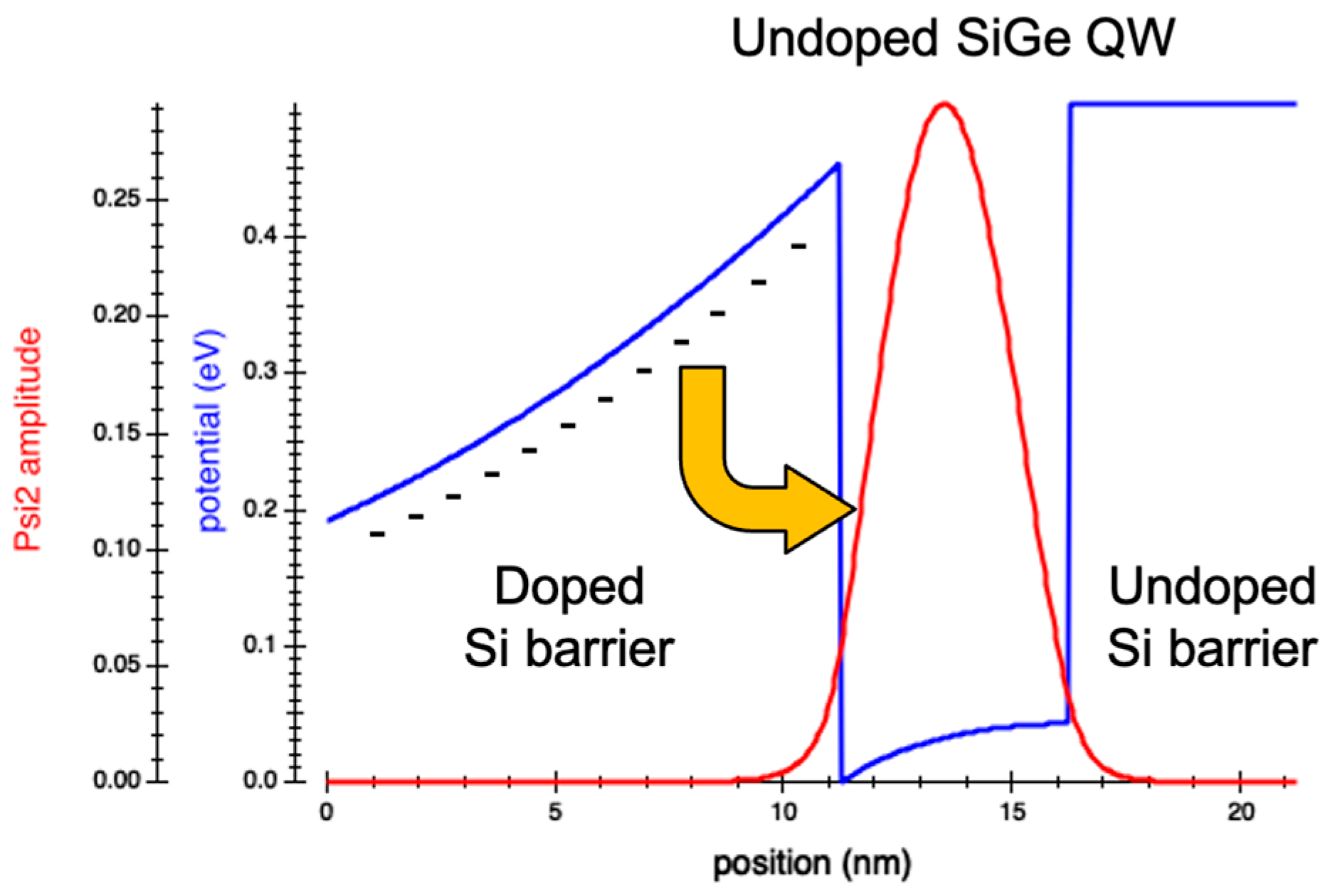
4.1. Design, Simulation Framework, and Material Parameters

A key point on series resistance reduction without an increase in optical loss in the Silicon Photonics phase shifter is to add the high-mobility overlayers on slab wings on both sides of the rib-waveguide core. High-mobility slab wings have thin overlayers consisting of a Si1−xGex/Si QW structure with x = 0.6, as illustrated in Figure 12. The phase shifter has been designed as a single-mode waveguide in TE-like mode in the C-band wavelength range for optical communication.
The phase shifter consists of a lateral PN-junction rib waveguide with a 480 nm width for the center rib, a 220 nm height for the center rib, and a 75 nm height for the side slab wing. The core is surrounded by bottom and top silica clads. The cross-section of the new phase shifter is simply the same as that of a commercially available PN-junction rib-waveguide phase shifter, except for slab wings topped up with heterojunction quantum-well overlayers. Special design refinement has been implemented to achieve both low series resistance and low optical loss. Pseudomorphic 5 nm Si1−xGex QW/5 nm Si barrier overlayers with x = 0.6 are formed on the slab wings. Si0.4Ge0.6 QW is strained and free from dislocations since the thickness of Si0.4Ge0.6 QW is thinner than the critical thickness [35]. High carrier mobility is achieved by eliminating dislocations, which act as scattering centers against carriers, and thus low electrical series resistance is realized. Pseudomorphic Si0.4Geo.6/Si heterojunction QW system yields type-II band line-up: holes are confined in the Si0.4Geo.6 overlayer, while electrons are in the Si overlayer [36].
The Silica gap between the edge of Si0.4Ge0.6/Si QW overlayers and the side wall of the rib is 100 nm in horizontal width. The silica gap is indispensable for suppressing the overlap of the modal electric field with the QW overlayers, in which high-density carriers are confined and thus high optical loss is produced via free-carrier absorption for the overlapping portion of the modal electric field. By virtue of the conservation of electric flux density and large discontinuity in the modal electric field along the horizontal direction, as predicted from Maxwell’s equations, the portion of the electric field of TE mode in the Si0.4Ge0.6/Si overlayers is very low as observed in the electric-field profile of TE fundamental mode in Figure 12. The mode-field profile is almost the same as that in the PN-junction rib waveguide without the QW overlayers. Therefore, optical loss due to 2D QW carriers is very low as described in the next subsection. Optical mode associated with such discontinuity in the modal electric field was observed in a slot waveguide consisting of a nanometer-scale slot of low refractive index [37].
Fabrication of the QW overlayers can be accommodated easily in CMOS-based fabrication processes in Figure 4. Two-step selective deposition processes of a 5 nm Si0.4Ge0.6 layer and, subsequently, a 5 nm Si layer to grow the overlayers on the top of Si slab wings before the VIA-hole fabrication step (10). Therefore, PN-junction rib-waveguide phase shifters can be designed and fabricated on the existing Silicon Photonics platform.
The distribution of the QW carriers along the vertical direction is determined as a quantum-mechanical wavefunction, which is a solution of the 1D Schrödinger equation. Therefore, the 1D Schrödinger equation needs to be solved. Numerical solutions of the 1D Schrödinger equation for the QW carriers in this paper were obtained by Noumerov’s method [38,39]. This method can be represented also in matrix form and is similar to the numerical eigenvalue method solving the discretized Schrödinger matrix [40,41]. The squared wavefunction of holes in the valence band of a 5 nm Si0.4Ge0.6 is plotted in Figure 13, in which the cross-section along the vertical axis on the P-type side is shown. The bottom p-type slab layer is located on the left side of the QW, and a 5 nm Si cap overlayer in the right side of the QW in the graph. Confinement potential was taken from the results of the TCAD simulation. Carriers confined in undoped Si0.4Ge0.6 QW are supplied and spatially separated from dopant atoms in the Si slab underneath the QW. The separation from the dopant atoms allows for the transport of QW carriers free from ionized impurity scattering and thus high carrier mobility in the QW. The conductivity effective mass used in the numerical calculation of the 1D Schrödinger equation is 0.1m0 for the hole. Here, m0 denotes the electron rest mass in free space [42]. The hole has a much lighter effective mass in strained Si0.4Ge0.6 than for electrons. Lighter hole mass allows hole quantum-mechanical wavefunction to penetrate doped Si barriers of the slab and the overlayer deeper. The conductivity effective mass of an electron is, on the other hand, almost the same as for Si, 0.34m0 [42]. Therefore, the hole in strained Si0.4Ge0.6 QW undergoes the effect of scattering potential of the dopant impurities more significantly than the electron.
In TCAD, Equations (2)–(6) are formulated in the framework of classical theory. The Schrödinger equation is not incorporated into classical TCAD to characterize quantum-mechanical features of carriers rigorously in numerical analysis. Alternatively, macroscopic methods have been developed for quantum-mechanical correction to classical TCAD simulation. The method taken in this paper is based on the Feynman–Hibbs effective potential derived from Feynman’s path-integral method to deal with quantum-mechanical motion in the classical framework [43,44,45]. Classical potential, Φ in Equation (2) is replaced with the Feynman–Hibbs effective potential, ΦFH, which is given as convolution of the classical potential with Gaussian function [43]:
Φ F H y = 1 2 π σ 2 m i n .   Y m a x .   Y d Y   Φ Y   e y Y 2 2 σ 2 .
Here, σ represents quantum-thermal width, which is written as
σ 2 = 2 12   m e f f   k B T ,
with reduced Planck constant, ħ, effective mass, meff, Boltzmann constant, kB, and temperature, T [44]. Quantum thermal width is about 2 nm for the hole conductivity effective mass quoted above. The quantum thermal width is substituted to the Feynman–Hibbs effective potential in the TCAD software program used to perform the simulation of carrier distribution and current flow in the phase shifter with quantum correction [45].
Band offsets of strained Si0.4Ge0.6 are 0.5 eV from the top of the valence band of Si for hole and 0.07 eV from the bottom of the conduction band of Si for electron, respectively [46]. Light hole and heavy hole masses are 0.1m0 and 0.2m0, respectively. Drift hole mobility in strained Si1−xGex was reported at x ranging from 0 to 0.3 [47]. The drift mobility increases linearly with x. Drift hole mobility at x = 0.6 is, thus, linear extrapolated from the reported data as high as 1750 cm2/V/s at a low dopant concentration of 1014 cm−3. Preset data in the TCAD software program have been used regarding the other material parameters [48].

4.2. Simulation Results and Discussion

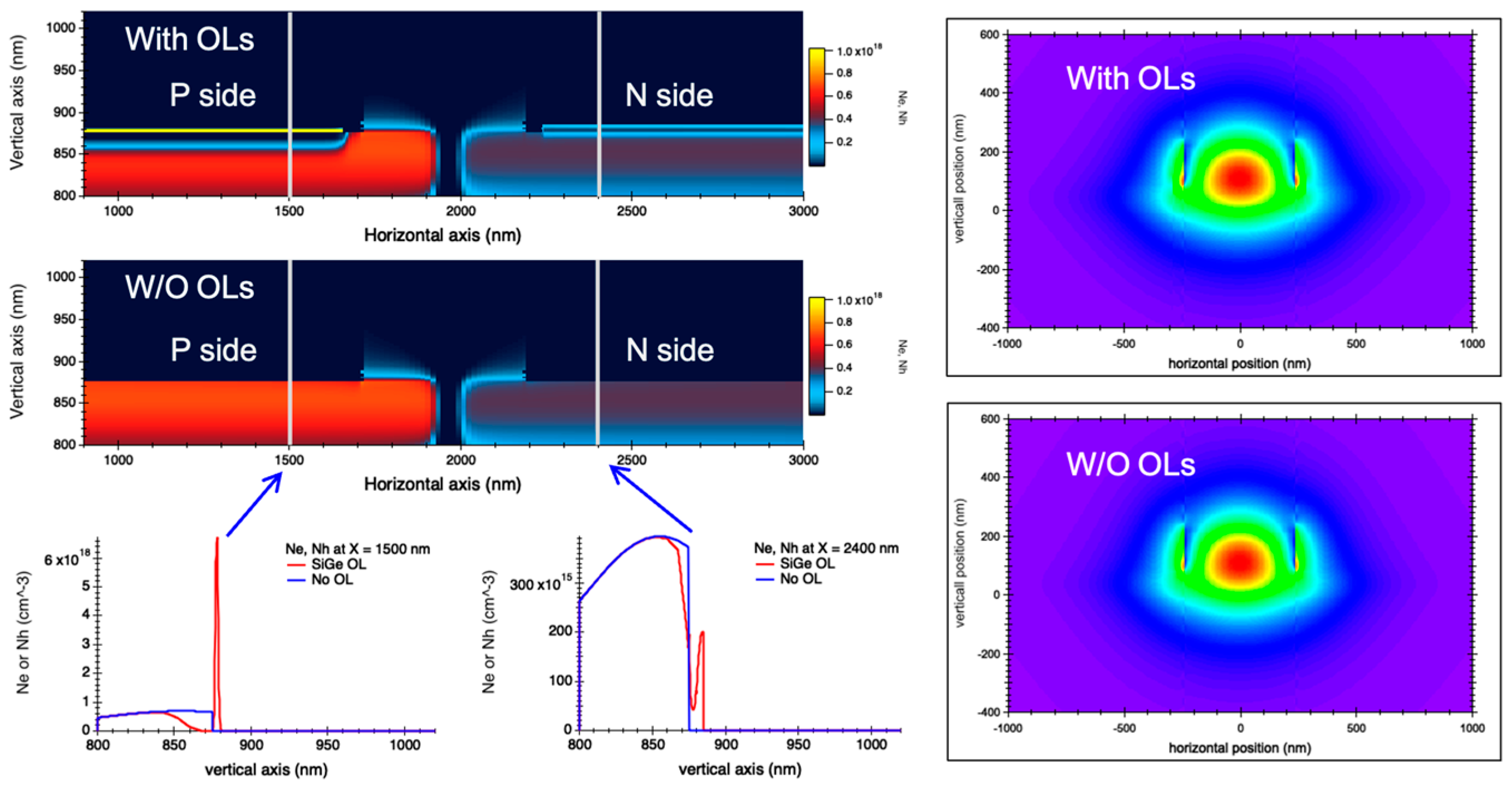
4.2.1. Carrier Distribution and Optical Loss

Hole and electron distribution profiles in the PN-junction phase shifter with and without QW overlayers are plotted in the color contrast scale in Figure 14. These profiles have been obtained at zero DC bias voltage in the TCAD simulation described above. Hole and electron distribution profiles in the cross-section at X = 1500 nm and 2400 nm in the horizontal axis are plotted, respectively. The horizontal center of the 480 nm rib waveguide is located at X = 1950 nm. In the phase shifter without the QW overlayers, carrier distribution profiles are similar to those obtained in the conventional phase shifters [28]. In the phase shifter with QW overlayers, however, holes are confined in high density in the Si0.4Ge0.6 layer. The confined carriers are supplied from the dopants in the P-type slab wing and the P-type slab region underneath the QW is depleted. The profile of hole distribution in the cross-section at X = 1500 nm reflects the spatial expansion of the quantum-mechanical wavefunction of the hole in Figure 13. Electrons in the N-type slab wing are confined in Si overlayer due to type-II band arrangement. The density of electrons in the Si layer is not high since the conduction-band offset is much smaller than the valence-band offset in potential energy.
Modal optical losses in the phase shifters with and without the QW overlayers are calculated from the overlap of the absolute square of the mode electric field with the optical-loss distribution associated with free-carrier absorption in the phase shifters. Carrier-density dependence of optical loss due to free-carrier absorption, Δα, at a wavelength of 1550 nm is written as [21]
α N e ,   N h = 8.88 × 10 21 N e 1.167 + 5.84 × 10 20 N n 1.109 .
Modal optical loss, Δαmode, is then calculated with the mode electric field, Emode, in the following equation:
α m o d e = d x d y α N e x ,   y ,   N h x ,   y   E m o d e x ,   y 2 d x d y E m o d e x ,   y 2
Profiles of the mode electric field with and without the overlayers in Figure 14 are almost the same as each other, as the overall thickness of the overlayers is as thin as 10 nm, and penetration of mode electric field to the overlayers is suppressed by the narrow silica gap between the overlayer edge and the rib side wall. Therefore, optical loss due to free carrier absorption associated with high-density 2D carriers in the QW overlayers is not as large as mentioned in the previous subsection. The modal optical loss is 2.93 dB/cm in the phase shifter with the overlayers, while 2.88 dB/cm in that without the overlayers. Almost the same modal loss has been obtained regardless of the addition of the overlayers.

4.2.2. Series Electrical Resistance

Reduction in electrical resistance has been confirmed in the simulation of DC current–voltage (I–V) characteristics. Models for DC I–V characterization are P-type and N-type test elements, respectively, which are displayed in the top part of Figure 15. The test elements consist of the QW overlayers in a width of 3400 nm along the X direction. Length along the Z axis, which is perpendicular to the X and Y axes, is 200 nm. The structure is uniform along the Z axis. Aluminum electrodes at both ends are connected to the surfaces of heavily doped regions, P++ and N++ (1 × 1020 cm−3) in a 75 nm Si slab layer. The electrical resistance of 5.59 Ω is obtained from DC I-V characteristics in the left bottom part in Figure 15 for the P-type Si slab layer with the QW overlayers if it is rescaled to 1 mm in length along the Z axis, while 31.0 Ω without the QW overlayers. The electrical resistance of the test element with the QW overlayers is lower than 1/5 times in comparison with that without the QW overlayers. For the N-type slab layer, electrical resistance reduction from 17.4 Ω to 15.9 Ω., namely about 10% reduction with the overlayers from DC I–V characteristics in the right bottom part of Figure 15. Resistance reduction is remarkable for holes because of their small effective masses and high-density confinement in the large band offset.
The next step in DC I–V characterization is to verify the series of electrical reductions in models of PN-junction rib-waveguide phase shifters with and without the QW overlayers. The model for the phase shifter with the QW overlayers is presented in the top part of Figure 16. The rib waveguide has a center rib with a 480 nm width and a 220 nm height and side slabs with a 75 nm height. The full width of the phase shifter along the X axis is 3900 nm. The width of QW overlayers is 1510 nm on each slab. The silica gap is 50 nm. The silica gap width can be 50–100 nm. Electrical and optical characteristics are not affected significantly by variation in the silica gap width from 50 to 100 nm. This leads to the allowance of overlay tolerance, +/−25 nm for lithographic misalignment in fabrication. The gap between a metal electrode and an edge of QW overlayers is also 50 nm. The structure along the Z axis is uniform and 200 nm in length. Simulation of DC I–V characteristics has been performed under forward bias voltage since there is no current flow and thus no voltage drop at series electrical resistors under reverse bias voltage. The equivalent circuit of the phase shifters is represented as a diode with series resistors, RP and RN, as shown in Figure 16. Red and blue curves correspond to DC current in forward-biased phase shifter with and without the QW overlayers, respectively. DC current at the low forward voltage is a thermally excited current over PN-junction potential, qVPN, and increases exponentially with applied DC voltage, V. Higher DC current implies that more DC bias is applied to PN junction as a result of lower series resistances, hence, lower voltage drops at the series resistors. The increase in DC voltage applied to the PN junction is more than 2 times. Therefore, the total series resistance, RP + RN, is estimated to be reduced by 1/2 times or lower with the QW overlayers, which is consistent with series resistances obtained in DC I–V characteristics of the test elements consisting of sheet resistors.

4.2.3. Modulation Bandwidth

Modulation bandwidth characteristics of the phase shifters are evaluated in electro-optic (EO) response as a function of modulation frequency for an equivalent circuit consisting of a capacitor, C connected with series resistors, RP, RN, as shown in Figure 17. EO response in the zero-frequency limit is equal to the optical losses obtained for the phase shifters in Section 4.2.1. Assuming an extension of a slab wing along the X axis to be 900 nm in each of the P and N sides, the total series resistance is 5.69 Ω and 12.8 Ω with and without the QW overlayers in 1 mm length along the Z axis, respectively. Under the reverse bias voltage applied to the PN junction of the phase shifters, junction capacitance is 0.35 pF/mm [49]. Substituting these circuit parameters to the circuit equation consisting of the lumped elements, EO response curves in Figure 17 are obtained in the small-signal circuit model [50]. A 3 dB bandwidth of EO response for the phase shifter with the QW overlayers is as high as 105 GHz, reaching a modulation speed of 200 Gbaud symbol rate in NRZ format. Modulation bandwidth is doubled in comparison with that without the overlayers, while optical loss is unchanged regardless of high-density 2D carriers in the overlayers. Thereby, the optical modulation bandwidth–optical loss trade-off is resolved with the PN-junction rib-waveguide phase shifter having the QW overlayers in side slab wings. This newly designed phase shifter allows for the performance enhancement of Silicon Photonics modulator in modulation speed in applications to high-capacity optical networks as ecosystems.

5. Conclusions

Limiting factors on modulation speed for integrated modulators on the Silicon Photonics platform have been addressed. Electrical resistance–capacitance coupling in PN-junction rib-waveguide phase shifter is shown to be the most crucial and to dominate modulation bandwidth among the limiting factors. Optical modulation bandwidth–optical loss trade-off arises from the resistance–capacitance coupling. High-mobility 2D carriers in QW overlayers added on side slab wings allow remarkable series resistance reduction and thus bandwidth expansion in optical modulation, as confirmed in numerical analysis based on mode electric field simulation and classical TCAD simulation with quantum-mechanical correction using Feynman–Hibbs effective potential. Optical loss due to free-carrier absorption is not increased regardless of high-density 2D carriers located in the QW overlayers because of the total thickness of the overlayers as thin as 10 nm and suppression of penetration of mode electric field to the overlayers by the narrow silica gap separating the overlayers from the rib side wall. Expansion of modulation bandwidth, namely the enhancement of modulation speed without causing an optical loss in the phase shifter available on the Silicon Photonics platform is finally confirmed. Silicon Photonics modulators including the PN-junction rib-waveguide phase shifters with QW overlayers can be designed and fabricated in the Silicon Photonics platform.

Funding

This research was funded in part by Fujitsu Optical Compenents Limited. The APC was funded by 6ca828dc52914eb7.

Data Availability Statement

The original contributions presented in the study are included in the article, further inquiries can be directed to the corresponding author.

Acknowledgments

The author would like to thank N. Nishiyama of the Tokyo Institute of Technology for his management and support of the research project regarding the subject studied in this paper. The author also would like to acknowledge S. Akiyama, K. Takabayashi, and N. Mitamura of Fujitsu Optical Components Limited for their support of research funding and technical discussions on phase-shifter design, and C.E. Png of the Institute of High-performance Computing, Singapore, for technical discussion on methodology regarding quantum-mechanical correction to classical TCAD simulation.

Conflicts of Interest

The author declares no conflict of interest.

References

  1. Gardes, F.Y.; Reed, G.T.; Emerson, N.G.; Png, C.E. A sub-micron depletion-type photonic modulator in Silicon on Insulator. Opt. Express 2005, 13, 8845–8854. [Google Scholar] [CrossRef]
  2. Pinguet, T.; Sadagopan, V.; Mekis, A.; Analui, B.; Kucharski, D.; Gloeckner, S. A 1550 nm, 10 Gbps optical modulator with integrated driver in 130 nm CMOS. In Proceedings of the 2007 4th IEEE International Conference on Group IV Photonics, Tokyo, Japan, 19–21 September 2007; pp. 1–3. [Google Scholar]
  3. Liao, L.; Liu, A.; Rubin, D.; Basak, J.; Chetrit, Y.; Nguyen, H.; Cohen, R.; Izhaky, N.; Paniccia, M. 40 Gbit/s silicon optical modulator for highspeed applications. Electron. Lett. 2007, 43, 1196–1197. [Google Scholar] [CrossRef]
  4. Marris-Morini, D.; Rasigade, G.; Vivien, L.; Cassan, E.; Laval, S.; Rivallin, P.; Lyan, P.; Fedeli, J.M. Recent progress in fast silicon modulators. In Proceedings of the 2008 5th IEEE International Conference on Group IV Photonics, Sorrento, Italy, 17–19 September 2008; pp. 1–3. [Google Scholar]
  5. Absil, P.; Croes, K.; Lesniewska, A.; De Heyn, P.; Ban, Y.; Snyder, B.; De Coster, J.; Fodor, F.; Simons, V.; Balakrishnan, S.; et al. Reliable 50 Gb/s Silicon Photonics platform for next-generation data center optical interconnects. In Proceedings of the 2017 IEEE International Electron Devices Meeting (IEDM), San Francisco, CA, USA, 2–6 December 2017; pp. 34.2.1–34.2.4. [Google Scholar]
  6. Giewont, K.; Hu, S.; Peng, B.; Rakowski, M.; Rauch, S.; Rosenberg, J.C.; Sahin, A.; Stobert, I.; Stricker, A.; Nummy, K.; et al. 300-mm Monolithic Silicon Photonics Foundry Technology. IEEE J. Sel. Top. Quant. Electron. 2019, 25, 1–11. [Google Scholar] [CrossRef]
  7. Fahrenkopf, N.M.; McDonough, C.; Leake, G.L.; Su, Z.; Timurdogan, E.; Coolbaugh, D.D. The AIM Photonics MPW: A Highly Accessible Cutting Edge Technology for Rapid Prototyping of Photonic Integrated Circuits. IEEE J. Sel. Top. Quant. Electron. 2019, 25, 1–6. [Google Scholar] [CrossRef]
  8. Siew, S.Y.; Li, B.; Gao, F.; Zheng, H.Y.; Zhang, W.; Guo, P.; Xie, S.W.; Song, A.; Dong, B.; Luo, L.W.; et al. Review of Silicon Photonics Technology and Platform Development. J. Light. Technol. 2021, 39, 4374–4389. [Google Scholar] [CrossRef]
  9. Ogawa, K. Integrated Silicon-Based Optical Modulators: 100/Gb/s and Beyond; SPIE Press: Bellingham, WA, USA, 2019. [Google Scholar]
  10. Ogawa, K.; Goi, K.; Tan, Y.T.; Liow, T.-Y.; Tu, X.; Fang, Q.; Lo, G.-Q.; Kwong, D.-L. Silicon Mach-Zehnder modulator of extinction ratio beyond 10 dB at 10.0–12.5 Gbps. Opt. Express 2011, 19, B26–B31. [Google Scholar] [CrossRef]
  11. Petousi, D.; Zimmermann, L.; Gajda, A.; Kroh, M.; Voigt, K.; Winzer, G.; Tillack, B.; Petermann, K. Analysis of Optical and Electrical Tradeoffs of Traveling-Wave Depletion-Type Si Mach–Zehnder Modulators for High-Speed Operation. IEEE J. Sel. Top. Quant. Electron. 2015, 21, 199–206. [Google Scholar] [CrossRef]
  12. Anderson, R.L. Germanium-Gallium Arsenide Heterojunctions. IBM J. Res. Dev. 1960, 4, 283–287. [Google Scholar] [CrossRef]
  13. Mimura, T.; Hiyamizu, S.; Fujii, T.; Nanbu, K. A New Field-Effect Transistor with Selectively Doped GaAs/n-AlxGa1-xAs Heterojunctions. Jpn. J. Appl. Phys. 1980, 19, L225–L227. [Google Scholar] [CrossRef]
  14. Hiyamizu, S.; Junji Saito, J.; Nanbu, K.; Ishikaw, T. Improved Electron Mobility Higher than 106 cm2/Vs in Selectively Doped GaAs/N-AlGaAs Heterostructures Grown by MBE. Jpn. J. Appl. Phys. 1983, 22, L609–L611. [Google Scholar] [CrossRef]
  15. Ando, T. Self-Consistent Results for a GaAs/AlxGa1-xAs Heterojunction. I. Subband Structure and Light-Scattering Spectra. J. Phys. Soc. Jpn. 1982, 51, 3898–3899. [Google Scholar] [CrossRef]
  16. Ando, T.; Fowler, A.B.; Stern, F. Electronic properties of two-dimensional systems. Rev. Mod. Phys. 1982, 54, 437–672. [Google Scholar]
  17. Ishikura, N.; Goi, K.; Zhu, H.; Illarionov, M.; Ishihara, H.; Oka, A.; Oda, T.; Masuko, K.; Ori, T.; Ogawa, K.; et al. Transmission characteristics of 32-Gbaud PDM IQ monolithic silicon modulator operating with 2-VPPD drive voltage. In Proceedings of the 42nd European Conference on Optical Communication (ECOC), Dusseldorf, Germany, 18–22 September 2016. [Google Scholar]
  18. Koyama, F.; Iga, K. Frequency chirping in external modulators. J. Light. Technol. 1988, 6, 87–93. [Google Scholar] [CrossRef]
  19. Han, J.; Seo, B.-J.; Han, Y.; Jalali, B.; Fetterman, H. Reduction of fiber chromatic dispersion effects in fiber-wireless and photonic time-stretching system using polymer modulators. J. Light. Technol. 2003, 21, 1504–1509. [Google Scholar]
  20. Goi, K.; Oda, K.; Kusaka, H.; Terada, Y.; Ogawa, K.; Liow, T.-Y.; Tu, X.; Lo, G.-Q.; Kwong, D.-L. 11-Gb/s 80-km transmission performance of zero-chirp silicon Mach-Zehnder modulator. Opt. Express 2012, 20, B350–B356. [Google Scholar] [CrossRef]
  21. Nedeljkovic, M.; Soref, R.; Mashanovich, G.Z. Free-carrier electrorefraction and electroabsorption modulation predictions for silicon over the 1–14-μm infrared wavelength range. IEEE Photonics J. 2011, 3, 1171–1180. [Google Scholar] [CrossRef]
  22. Goi, K.; Oka, A.; Kusaka, H.; Terada, Y.; Ogawa, K.; Liow, T.-Y.; Tu, X.; Lo, G.-Q.; Kwong, D.-L. Low-loss high-speed silicon IQ modulator for QPSK/DQPSK in C and L bands. Opt. Express 2014, 22, 10703–10709. [Google Scholar] [CrossRef]
  23. Goi, K.; Oda, K.; Mashiko, Y.; Ogawa, K.; Liow, T.-Y.; Tu, X.; Lo, G.-Q.; Kwong, D.-L. 128 Gb/s DP-QPSK Silicon Modulator Module Integrated with Driver Amplifiers. In Proceedings of the 2014 European Conference on Optical Communication (ECOC), Cannes, France, 21–25 September 2014. [Google Scholar]
  24. Li, X.; Gourikutty, S.B.N.; Wu, J.; Lim, T.G.; Guo, P.; Davies, J.C.; Koh, E.S.C.; Long, L.B.; Jong, M.C.; Li, C.; et al. 1.6 Tbps (224 Gbps/λ) Silicon Photonic Engine Fabricated with Advanced Electronic-Photonic FOWLP for Co-Packaged Optics and Linear Drive Applications. In Proceedings of the Optical Fiber Communication Conference, San Diego, CA, USA, 24–28 March 2024. [Google Scholar]
  25. Ostrovskis, A.; Szczerba, K.; Salgals, T.; Norberg, E.; Koenigsmann, M.; Sonkoly, J.; Rubuls, K.; Yun, H.; Krüger, B.; Piels, M.; et al. Heterogenous InP Electro-Absorption Modulator with Si Waveguides for Beyond 200 Gbps/λ Optical Interconnects. In Proceedings of the Optical Fiber Communication Conference, San Diego, CA, USA, 24–28 March 2024. [Google Scholar]
  26. St-Arnault, C.; Bernal, S.; Berikaa, E.; Wei, Z.; Gutiérrez-Castrejón, R.; Zhang, J.; Alam, S.; Nikic, A.; Krueger, B.; Pittalà, F.; et al. Net 1.6 Tbps (4×400Gbps/λ) O-Band IM/DD Transmission Over 2 km Using Uncooled DFB Lasers on the LAN-WDM grid and Sub-1V Drive TFLN Modulators. In Proceedings of the 2024 Optical Fiber Communications Conference and Exhibition, San Diego, CA, USA, 24–28 March 2024. [Google Scholar]
  27. Schwarzenberger, A.; Sarwar, S.; Eschenbaum, C.; Mertens, A.; Martens, M.; Kotz, A.; Fang, D.; Sherifaj, A.; Singer, S.; Kholeif, H.; et al. O-Band SOH Mach-Zehnder Modulator Operating at a PAM4 Line Rate of 384 Gbit/s with Sub-Volt Drive Voltage. In Proceedings of the 2024 Optical Fiber Communications Conference and Exhibition (OFC), San Diego, CA, USA, 24–28 March 2024. [Google Scholar]
  28. Png, C.E.; Sun, M.J.; Lim, S.T.; Ang, T.Y.L.; Ogawa, K. Numerical modeling and analysis for high-efficiency carrier-depletion silicon rib-waveguide phase shifters. IEEE J. Sel. Top. Quantum Electron. 2016, 22, 3300208. [Google Scholar] [CrossRef]
  29. Rigrod, W.W.; Kaminow, I.P. Wide-band microwave light modulation. Proc. IEEE 1963, 51, 137–140. [Google Scholar] [CrossRef]
  30. Liu, J. Photonic Devices; Cambridge University Press: Cambridge, UK, 2005; pp. 274–279. [Google Scholar]
  31. Yang, Y.; Fang, Q.; Yu, M.; Tu, X.; Rusli, R.; Lo, G.-Q. High-efficiency Si optical modulator using Cu travelling-wave electrode. Opt. Express 2014, 22, 29978–29985. [Google Scholar] [CrossRef]
  32. Xu, H.; Li, X.; Xiao, X.; Li, Z.; Yu, Y.; Yu, J. Bandwidth performances analysis for high-speed silicon depletion-mode modulator. In Proceedings of the OFC 2014, San Francisco, CA, USA, 9–13 March 2014. [Google Scholar]
  33. Allam, J.; Baynes, N.d.B.; Cleaver, J.R.A.; Ogawa, K.; Mishima, T.; Ohbu, I. Monolithically-integrated optoelectronic circuit for ultrafast sampling of a dual-gate field-effect transistor. Opt. Quant. Electron. 1996, 28, 875–896. [Google Scholar] [CrossRef]
  34. Xiao, X.; Li, M.; Li, Z.; Wang, L.; Yang, Q.; Yu, S. Substrate removed silicon Mach-Zehnder modulator for high baud rate optical intensity modulations. In Proceedings of the 2016 Optical Fiber Communications Conference and Exhibition (OFC), Anaheim, CA, USA, 20–24 March 2016. [Google Scholar]
  35. People, R. Physics and applications of GexSi1-x/Si strained-layer heterostructures. IEEE J. Quantum Electron. 1986, 22, 1696–1710. [Google Scholar] [CrossRef]
  36. Van de Walle, C.G.; Martin, R.M. Theoretical calculations of heterojunction discontinuities in the Si/Ge system. Phys. Rev. B 1986, 34, 5621–5634. [Google Scholar] [CrossRef]
  37. Almeida, V.R.; Xu, Q.; Barrios, C.A.; Lipson, M. Guiding and confining light in void nanostructure. Opt. Lett. 2004, 29, 1209–1211. [Google Scholar] [CrossRef]
  38. Noumerov, B.V. A Method of Extrapolation of Perturbations. Mon. Not. R. Astron. Soc. 1924, 84, 592–602. [Google Scholar] [CrossRef]
  39. Quiroz González, J.L.M.; Thompson, D. Getting started with Numerov’s method. Comput. Phys. 1997, 11, 514–515. [Google Scholar] [CrossRef]
  40. Pillai, M.; Goglio, J.; Walker, T.G. Matrix Numerov method for solving Schrödinger’s equation. Am. J. Phys. 2012, 80, 1017–1019. [Google Scholar] [CrossRef]
  41. Cooney, P.J.; Kanter, E.P.; Vager, Z. Convenient numerical technique for solving the one-dimensional Schrödinger equation for bound states. Am. J. Phys. 1981, 49, 76–77. [Google Scholar] [CrossRef]
  42. Kim, Y.; Takenaka, M.; Osada, T.; Hata, M.; Takagi, S. Strain-induced enhancement of plasma dispersion effect and free-carrier absorption in SiGe optical modulators. Sci. Rep. 2014, 4, 4683. [Google Scholar] [CrossRef]
  43. Feynman, R.P. Space-Time Approach to Non-Relativistic Quantum Mechanics. Rev. Mod. Phys. 1948, 20, 367–387. [Google Scholar] [CrossRef]
  44. Doll, J.D.; Myers, L.E. Semiclassical Monte Carlo methods. J. Chem. Phys. 1979, 71, 2880–2883. [Google Scholar] [CrossRef]
  45. Voth, G.A. Calculation of equilibrium averages with Feynman-Hibbs effective classical potentials and similar variational approximations. Phys. Rev. A 1991, 44, 5302–5305. [Google Scholar] [CrossRef]
  46. Yang, L.; Watling, J.R.; Wilkins, R.C.W.; Boriçi, M.; Barker, J.R.; Asenov, A.; Roy, S. Si/SiGe heterostructure parameters for device simulations. Semicond. Sci. Technol. 2004, 19, 1174–1182. [Google Scholar] [CrossRef]
  47. Manku, T.; McGregor, J.M.; Nathan, A.; Roulston, D.J.; Noel, J.P.; Houghton, D.C. Drift hole mobility in strained and unstrained doped Si1−xGex alloys. IEEE Trans. Elect. Dev. 1993, 40, 1990–1996. [Google Scholar] [CrossRef]
  48. 3-Dimensional TCAD System Advance/TCAD. Available online: https://www.advancesoft.jp/products/semiconductor/advance-tcad/ (accessed on 2 May 2024). (In Japanese).
  49. Liow, T.-Y.; Ang, K.W.; Fang, Q.; Song, J.F.; Xiong, Y.Z.; Yu, M.B.; Lo, G.Q.; Kwong, D.L. Silicon Modulators and Germanium Photodetectors on SOI: Monolithic Integration, Compatibility, and Performance Optimization. IEEE J. Sel. Top. Quant. Electron. 2010, 16, 307–315. [Google Scholar] [CrossRef]
  50. LTspice. Available online: https://www.analog.com/en/resources/design-tools-and-calculators/ltspice-simulator.html (accessed on 7 May 2024).
Figure 1. (a) Optical-microscope top-view photograph of PDM IQ integrated Silicon Photonics modulator chip; (b) schematic waveguide layout of the PDM IQ modulator in the photograph; (c) illustrated single Silicon Photonics MZ modulator; (d) configuration of an IQ MZ modulator.
Photonics 11 00535 g001
Figure 2. PN-junction rib-waveguide phase shifter. The illustrated cross-section with schematic depletion region (gray) and mode field (yellow) in the middle.
Photonics 11 00535 g002
Figure 3. Cross-sections of passive and active blocks of Silicon Photonics modulators integrated with Ge monitor PDs fabricated using SOI wafer.
Photonics 11 00535 g003
Figure 4. Fabrication process flow of PN-junction rib-waveguide phase shifter. Gray, red, and green arrows indicate dry etching, implantation of P-type dopants, and implantation of N-type dopants, respectively.
Photonics 11 00535 g004
Figure 5. DC measurement and simulation characteristics of the phase shifter and the Silicon Photonics MZ modulator.
Photonics 11 00535 g005
Figure 6. (a) Packaged PDM IQ integrated Silicon Photonics modulator; (b) measured constellation diagrams in the advanced modulation formats of QPSK, 16 QAM, and 32 QAM in orthogonal polarization components, X and Y.
Photonics 11 00535 g006
Figure 7. Modulation performances of the integrated Silicon Photonics modulators in bit rate and symbol rate of 200 Gbaud and beyond prospected for the Silicon Photonics modulator with speed enhancement described in Section 4. * A 112 Gbaud modulation reported recently for parallel-lane Silicon Photonics modulators after wafer-level co-packaging [24].
Photonics 11 00535 g007
Figure 8. (a) Input electrical bias voltage with 1 ps linear ramps. (b) Cross-section of lateral PN-junction phase shifter as simulation model and transient of effective refractive index change in the phase shifter obtained in the simulation. (c) The rise and fall edges of the transient of the effective refractive index in (b).
Photonics 11 00535 g008
Figure 9. Conceptual display of velocity mismatch between optical wave packet and RF electrical wave in Silicon Photonics MZ modulator.
Photonics 11 00535 g009
Figure 10. Electro-optical frequency responses characteristics of Silicon Photonics modulator.
Photonics 11 00535 g010
Figure 11. Equivalent circuit models for carrier-depletion rib-waveguide phase shifter and traveling-wave modulator including carrier-depletion phase shifter.
Photonics 11 00535 g011
Figure 12. Schematic cross-section of rib-waveguide phase shifter with QW slab wings.
Photonics 11 00535 g012
Figure 13. Squared quantum-mechanical wavefunction of holes (red) in classical valence-band potential (blue) of selectively doped Si slab/undoped Si0.4Ge0.6 QW/Si barrier.Yellow arrow indicating flow of holes from dopants in the barrier to the QW.
Photonics 11 00535 g013
Figure 14. Profiles of electron and hole distribution profiles and mode electric field in PN-junction phase shifter with and without QW overlayers (OLs) (left). Hole and electron distribution at cross sections at X = 1500 nm and 2400 nm (right). Profiles of fundamental mode-field TE polarization with and without QW overlayers on the right.
Photonics 11 00535 g014
Figure 15. Model test element with the QW overlayers (top) and DC I–V characteristics of test elements with and without QW overlayers (bottom).
Photonics 11 00535 g015
Figure 16. Model of DC I–V simulation (top) and DC I–V characteristics of the phase shifters with and without QW overlayers under forward bias voltage (bottom).
Photonics 11 00535 g016
Figure 17. Numerical EO response of PN-junction phase shifter represented as lumped-element circuit.
Photonics 11 00535 g017
Disclaimer/Publisher’s Note: The statements, opinions and data contained in all publications are solely those of the individual author(s) and contributor(s) and not of MDPI and/or the editor(s). MDPI and/or the editor(s) disclaim responsibility for any injury to people or property resulting from any ideas, methods, instructions or products referred to in the content.

