Article

High-Performance Terahertz Coherent Perfect Absorption with Asymmetric Graphene Metasurface

1
Department of Physics, School of Physics and Material Science, Nanchang University, Nanchang 330031, China
2
Institute of Space Science and Technology, Nanchang University, Nanchang 330031, China
3
School of Physics, Nankai University, Tianjin 300071, China
4
Collaborative Innovation Center of Extreme Optics, Shanxi University, Taiyuan 030006, China
*
Authors to whom correspondence should be addressed.
Photonics 2024, 11(6), 544; https://doi.org/10.3390/photonics11060544
Submission received: 9 May 2024 / Revised: 25 May 2024 / Accepted: 3 June 2024 / Published: 7 June 2024
(This article belongs to the Special Issue Advanced Lasers and Their Applications II)

Abstract

:
In this work, we introduce a novel coherent perfect absorber, accentuating its novelty by emphasizing the broad bandwidth, reduced thickness, tunable property, and straightforward design achieved through the use of an asymmetric graphene metasurface. This design incorporates both square and circular graphene patches arranged on either side of a silicon substrate. With an optimized structural design, this absorber consistently captures over 90% of incoming waves across the frequency range of 1.65 to 4.49 THz, with a graphene Fermi level of 0.8 eV, and the whole device measures just 1.5 um thick. This makes our absorber significantly more effective and compact than previous designs. The absorber’s effectiveness can be significantly enhanced by combining the metasurface’s geometric design with the graphene Fermi level. It is anticipated that this ultrathin, wideband coherent perfect absorption device will play a crucial role in emerging on-chip THz communication technologies, including light modulators, photodetectors, and so on.

1. Introduction

High technology advancements have made electromagnetic absorption a major research focus [1]. Coherent perfect absorption (CPA) is a promising phenomenon where two coherent light beams, illuminating from opposite sides of a medium or structure, interfere in such a way that the medium or structure absorbs all the incoming light, resulting in no reflection or transmission [2,3,4,5]. This process hinges on the precise control of the phase and amplitude of the light beams to achieve perfect absorption through coherent interference. CPA can be realized through various structures, including thin films and waveguides, offering more absorption tunability through interference interactions compared to perfect absorbers that rely on strong resonance [6,7]. Numerous CPA structures have been designed and experimentally validated for a wide range of frequencies, from microwave to optical [8,9,10,11,12,13]. This makes them highly promising for applications in electromagnetic modulation, switching, and signal processing.
The simplest structure for achieving CPA is a thin film or flat plate. Two-dimensional (2D) materials [14], such as graphene, are ideal for this purpose due to their ultrathin profile and excellent electrical properties [15,16,17]. Graphene, a 2D mono-layer of carbon atoms, has exceptional optical and electrical properties [18,19]. It has been widely used in various optical devices, including polarizers, phase shifters, and absorbers, due to its ability to manipulate the interaction between light and matter [20,21,22]. However, the absorption rate of single-layer graphene is only 2.3% [18,23], which is determined by its thin-layer conductivity. To improve the bandwidth and reduce the thickness of the CPA structure, researchers have explored the theory of CPA in patterned graphene structures, such as square graphene ring- and T-shaped graphene structures [24,25,26,27]. The graphene metasurface-based CPA system enhances incident light absorption and widens the absorption bandwidth [25,28,29]. An asymmetric graphene metasurface structure has been developed to achieve CPA, and it has a 90% absorption bandwidth of 1.5 THz and a thickness of only 2 um [30]. Additionally, the performance of the graphene metasurface can be dynamically controlled by varying the graphene Fermi level through using electrostatic gating or chemical doping, resulting in a wide frequency tunable range [31,32]. Moreover, the graphene metasurface structure is also suitable for small-scale integration.
In this study, an ultrabroadband THz CPA structure is proposed based on an asymmetric graphene metasurface, which consists of both square and circular graphene patches arranged on opposite sides of a silicon substrate. The results show that with a graphene Fermi level of 0.8 eV, this designed asymmetric structure can achieve an over 90% absorption bandwidth of 2.84 THz, ranging from 1.65 to 4.49 THz. In comparison to previously reported CPA structures, the absorption performance of this new metamaterial absorber is significantly enhanced, while its structure is relatively simpler. The effects of phase difference between two coherent lights, the structural geometry, and the incident angle on the CP performance are demonstrated in detail. Importantly, we achieve CPA tunability by varying the graphene Fermi level. This ultrathin, wideband coherent perfect absorption device is expected to have a significant impact on the development of on-chip THz communication technologies such as light modulators, sensors, and photodetectors.

2. CPA Theory and Design of Ultrabroadband CPA with Graphene Metasurfaces

Figure 1a depicts the configuration of a unit cell of the graphene metasurface, which consists of arrays of square and circular graphene patches positioned on opposite sides of a silicon substrate. It is illuminated by two counter-propagating and coherently modulated optical beams, designated as Ein1 and Ein2, with Eout1 and Eout2 representing the corresponding output waves. By optimizing the proposed structure to have specific reflection and transmission coefficients from singe-side illumination, the CPA conditions can be satisfied. We need to deduce the CPA conditions via the scattering matrix S by linking the outgoing waves Eout1 and Eout2 with the incident waves Ein1 and Ein2. The formula can be described as follows [33,34]:
E o u t 1 E o u t 2 = S E i n 1 E i n 2 = r 1 t 1 t 2 r 2 E i n 1 E i n 2
where r1, r2, t1, and t2 are the reflection coefficients and transmission coefficients of incident waves Ein1 and Ein2, excited on the front and back sides of the metasurface structure, respectively. Since this configuration does not break the reciprocity, the transmission coefficient is equal from both incident directions, i.e., t = t1 = t2. For symmetric coherent illumination, we have E in 1 = E in 2 e i θ , where θ is the phase difference between the two incident waves. To quantitatively investigate CPA, we define the absorption coefficients as:
A = 1 E out 1 2 + E out 2 2 E in 1 2 + E in 2 2
By deriving from Equation (2), the absorption coefficient can be simplified to the following:
A = 1 r 1 e i θ + t 2 + t e i θ + r 2 2 2
The CPA operation implies that the absorption coefficients are equal to 1. As a result, the conditions to achieve CPA should be r 1 = t e i θ and r 2 = t e i θ . In order to achieve CPA, we need to optimize the proposed structure to meet the CPA conditions.
Figure 1. (a) Schematic for a unite cell of an asymmetric graphene metasurface illuminated by two counter-propagating and coherently modulated input waves, Ein1 and Ein2. (b) Schematic of an ion gel-gating approach used to dope the graphene patch array.
Photonics 11 00544 g001
This configuration in Figure 1a induces considerable structural asymmetry, which, in turn, broadens the bandwidth of the CPA response. Design optimization was conducted through numerical simulations using COMSOL Multiphysics. In the numerical simulations, a 3D model was constructed, and periodic boundary conditions were applied along the x and y directions, reflecting the finite periodicity of the proposed structure in these dimensions. Port boundary conditions are placed in the z direction to create the incident plane wave, which is assumed to be polarized along the x-axis, i.e., transverse magnetic (TM) polarization. The parameters of the optimized design are detailed in Figure 1a; the square graphene patch length l is 5 um, the circular graphene patch radius r is 1.5 um, the silicon substrate thickness t is 1.5 um, and the structure’s period p is 5.2 um. The proposed CPA structure can be easily fabricated in potential experiments. Single-layer graphene can be cultivated on copper substrates via chemical vapor deposition. Graphene in square and circular forms can be achieved through the use of photoresist techniques, electron beam exposure, and plasma etching processes [35]. Furthermore, silicon films of micron thickness can be acquired by mechanically grinding, polishing, and etching thick monocrystalline silicon [36]. To modulate the graphene metasurface, an ion gel with a low relative permittivity of 1.82 can be employed as the gate dielectric material atop the graphene metasurfaces. Two gold gate contacts can be fabricated on the ion gel layers [37,38,39,40], as depicted in Figure 1b, to apply voltage, dope the graphene, and thereby tune the absorption response. Owing to the thin thickness and low permittivity of the ion gel layers, their impact on the system’s performance was determined to be negligible (not illustrated here) and was therefore disregarded in our simulations.
Due to graphene’s planar nature, it is modeled as a surface current in our simulations, described as J = σg(w)E, where σg is the conductivity of the graphene, and E is the electric field along the graphene surface. Graphene conductivity can be modulated by chemical doping or external electric field bias, and it is defined as follows [41]:
σ g ω = σ intra ω + σ inter ω
σ intra ( ω ) = 2 e 2 k B T π 2 i ω + i τ 1 ln 2 c o s h E F 2 k B T
σ inter ω = e 2 4 1 2 + 1 π a r c t a n ω 2 E F 2 k B T i 2 π ln ω + 2 E F 2 ω 2 E F 2 + 4 k B T 2
where σ intra ( ω ) and σ inter ( ω ) represent the intra- and inter-band transition conductivities, e is the electron charge, kB is the Boltzmann constant,  is the Plank’s constant, T is the Kelvin temperature, τ is the relaxation time, and EF is the Fermi level. In the low-THz range, intra-band transitions dominate the graphene response, and the graphene conductivity can be expressed by use of the Drude model [42]:
σ g ( ω ) = e 2 E F π 2 i ω i τ 1
Here, the relaxation time is assumed to be 10−13 s.

3. Results and Discussion

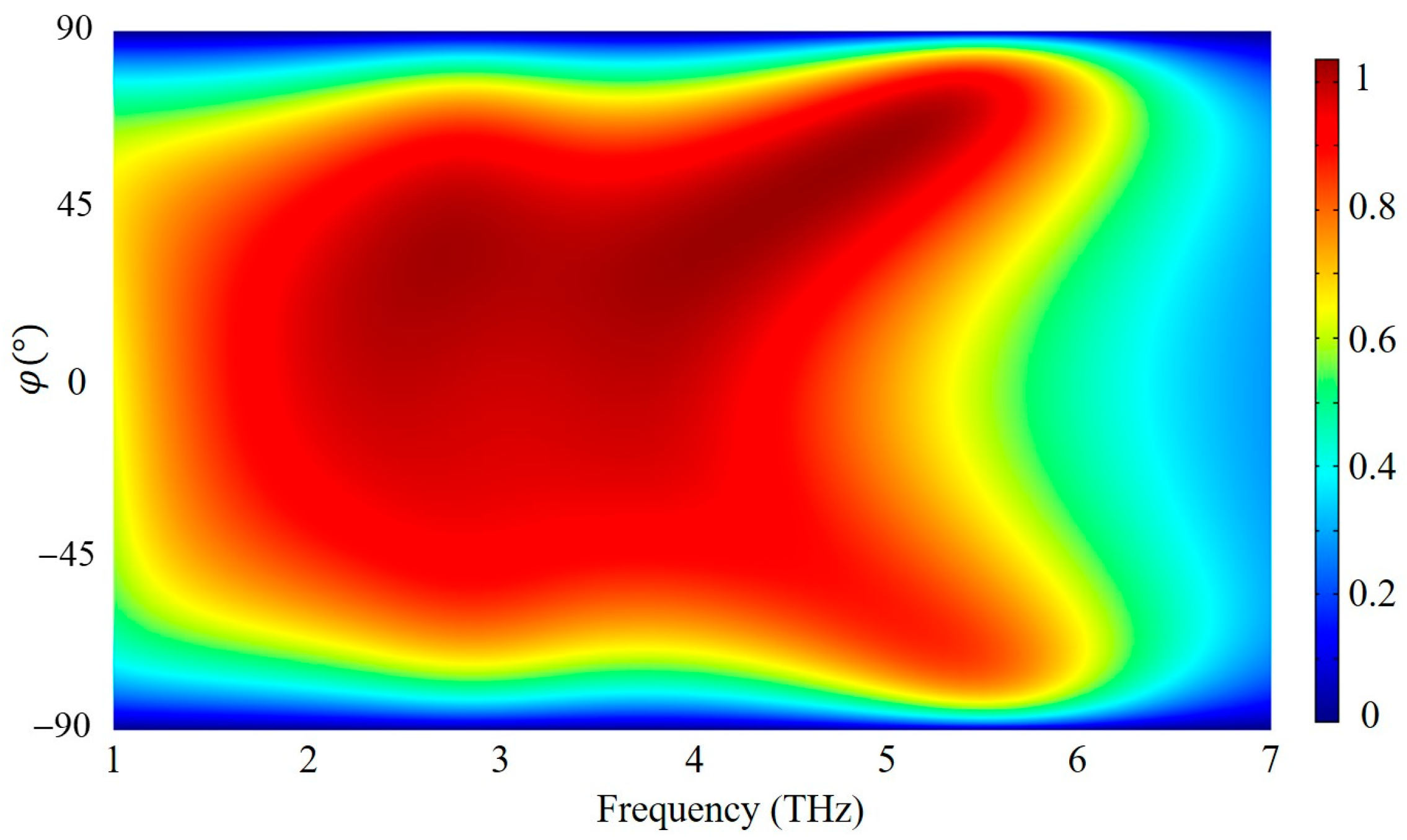
3.1. Results of Broadband Absorber

Here, we initially investigate single illumination on the proposed asymmetric metasurface. The spectral responses, including reflection, transmission, and absorption, under normal incidence for both front and back illuminations are depicted in Figure 2a and Figure 2b, respectively. The Fermi level of graphene EF is 0.8 eV. It is clear that the transmission from both sides is identical because reciprocity is not broken with this designed configuration. However, reflection and absorption are different due to the structural asymmetry. As illustrated in Figure 2a,b, at a frequency of 2.5 THz, the absorption coefficient for the front illumination is A1 = 45.2%. For the back illumination, the absorption coefficient is A2 = 52.4%. At a frequency of 3.7 THz, the absorption coefficients for the front and back illuminations are A1 = 44.1% and A2 = 55.5%, respectively. We find that the 50% absorption bound is broken for the back illumination due to the proposed extremely asymmetric structural design. Furthermore, across a broad frequency range, the absorption for a single incident wave from either direction approaches 50%, which lays an important groundwork for realizing the broadband CPA response.
Next, two counter-propagating TM-polarized incident waves illuminate the proposed design normally from the front and back sides simultaneously. Controlling phase difference is very important in achieving the CPA effect; since identical-amplitude coherent illumination was utilized in this work. By varying the phase difference θ between the two incident waves, we aimed to satisfy the CPA condition [34] and achieve perfect absorption. Figure 3a illustrates the calculated absorption coefficient [26] as a function of the operating frequency and phase difference θ between the two input waves. It can be found that over a wide range of frequencies, nearly perfect absorption is obtained when the phase difference θ is smaller than 30°. Importantly, by tuning the phase difference between the incident waves, the absorption coefficients can be modulated from 0 to 99.7% at 2.5 THz and to 99.8% at 3.7 THz. This implies that a coherent beam traversing the CPA structure can be modulated from near-complete absorption to near-complete transparency. The modulation depth (MD) [4,30,43] is a convenient figure of merit for evaluating the performance of the proposed structure for use in devices such as modulators, switches, or detectors. It can be calculated as MD = (Amax − Amin)/Amax, where Amax and Amin are the maximum and minimum of absorption from phase modulation or Fermi level modulation. Here, the MD can reach as high as 0.997 at both 2.5 THz and 3.7 THz through phase modulation. These findings could enable a host of potential applications, including planar terahertz modulators and graphene-based coherent photodetectors [44]. To effectively illustrate the excellent absorption capability of our design, we have set the phase difference constant to compute the relevant output coefficient across various frequencies. Here, we select a specific angle, θ = 0°, as it aligns with the best absorption performance, marked by the destructive interference of the two incoming waves. The outcomes are graphically represented in Figure 3b, showcasing a distinct broadband CPA response with an impressive ≥90% absorption coefficient spanning a broad frequency spectrum from 1.65 THz to 4.49 THz. Note that the same broadband CPA response can be achieved with this structure under TE-polarized incidence, since the structure is symmetric along the x-axis and y-axis.
Our analysis suggests that the wideband CPA response arises due to the hybridization and coupling of narrowband resonant CPA responses from differently shaped graphene patch arrays on the front and back sides. To verify this analysis, we calculated the absorption coefficients for a structure featuring a single-sided graphene patch array. Figure 4a shows the calculated absorption of the structure with a square graphene patch array solely on the front side of the silicon substrate. It can be observed that a single resonance occurs at 2.34 THz. By optimizing the length l of the square graphene patches, the resonance shifts to 2.47 THz at l = 4.9 um, and the absorption coefficient approaches 1. With a solely circular graphene patch array, a single resonance persists at 3.77 THz, and the absorption coefficient reaches 70.5%, as shown in Figure 4b. We further optimized the structure by adjusting the radius r of the circular graphene patches. The absorption coefficient can reach 99.7% with r = 2.5 um, yet it remains a single resonance. It is implied that broadband response cannot be achieved without efficient coupling between two patch arrays on both sides of the substrate. To further illustrate the impact of structural asymmetry on the broadband absorption effect, here, we compare symmetric and asymmetric bifacial graphene metasurfaces. The result is shown in Figure 4c,d. Figure 4c illustrates the absorption coefficient for a design with square graphene patch arrays on both sides of the substrate. The red line represents the absorption coefficient with a patch length of 5 μm (a value used for the square patch in the asymmetric design), while the blue line shows the result with an optimized radius of 4 μm for the symmetric design. This figure indicates that identical square patch arrays on both sides fail to achieve a broadband CPA effect, even with further optimization. Figure 4d displays the absorption coefficient for a design with identical circular graphene patch arrays on both sides of the substrate. The blue line, symbolizing the optimized symmetric structure, demonstrates that the symmetric design fails to meet the criteria for broadband coherent absorption. These results indicate that significant structural asymmetry is essential to achieving a wideband CPA response, given that a graphene metasurface design exhibiting minimal asymmetry will exhibit CPA only at a single resonant frequency.

3.2. Results of Tunable Absorber

Here, we investigate the impact of different geometric parameters on the absorptivity of the asymmetric graphene metasurface. It is imperative to examine the effects of the silicon thickness t, the radius r of the circular patches, and the length l of the square patches on absorption characteristics. The corresponding simulated results are depicted in Figure 5a–c. Figure 5a illustrates the absorption spectra generated by varying the silicon thickness with the parameters held constant at r = 1.5 um and l = 5 um. As the silicon thickness increases, the first resonance at the lower frequency remains virtually unchanged, yet there is a slight decrease in absorption amplitude. Conversely, the second resonance at the higher frequency exhibits a blueshift, accompanied by a significant decrease in the absorption coefficient. Optimal absorption bandwidth is attained at a silicon thickness of 1.5 um. Subsequently, the absorption at both resonances initially increases and subsequently decreases as we adjust the radius of the circular patches, starting from 1.1 um, with the silicon thickness and square patches length fixed at t = 1.5 um and l = 5 um, respectively, as shown in Figure 5b. Figure 5c presents the absorption spectra for varying square patch lengths with t = 1.5 um and r = 1.5 um. Increasing the length l causes the first resonance to redshift, enhancing the maximum absorption coefficient. The structure demonstrates optimal performance when the length reaches 5 um. When the square graphene patch entirely covers the silicon substrate, namely, when l equals 5.2 um, a single resonance is observed, as indicated by the light cyan line in Figure 5c, which resembles the performance of a single-side circular graphene patch. This result implies that a complete graphene sheet does not resonate with the excited electromagnetic waves. It is worth noting that in practical applications, small relative shifts between the centers of the rectangular and circular graphene components are inevitable during fabrication. We set out to clarify this issue by performing more simulations, and it turns out that the relative shift shows a limited effect on the broadband absorption response.
Tunability is a unique property of graphene-based structures which enables dynamic control of the coherent absorption in the proposed device by adjusting the graphene’s Fermi level EF. To demonstrate the tunability of the proposed CPA design, we calculated the output coefficients by sweeping EF from 0.1 eV to 1 eV. The results are shown in Figure 6. It can be observed that the CPA response can be achieved across a broad frequency range when the EF is greater than 0.3 eV, and as the EF increases, a blueshift in the resonant frequency is observed. This phenomenon can be attributed to graphene exhibiting more metallic behavior with the elevation of its Fermi level, which aligns with the established correlation between the resonant frequency and the Fermi level in graphene patches, which can be concisely represented as f r E F / L [21,30,45], with L denoting the side length of the graphene patch or the structural geometry. Moreover, we computed the MD by manipulating the graphene Fermi level, with the MD reaching a maximum of 0.88 at 2.5 THz and 0.94 at 3.7 THz. These results suggest that the graphene Fermi level is critical to the tunability of the absorption response, indicating that the structure functions as an efficient light modulator.
In practical applications, wide-angle absorption represents a crucial feature of absorbers. We investigated the impact of various incident angles on the absorption performance. Figure 7 illustrates the coherent absorption of the proposed asymmetric graphene metasurface as a function of the operating frequency and incident angle φ. Clearly, the absorption magnitude and bandwidth are well maintained until the incident angle increases to 45°, indicating that the absorption resonance is insensitive to small incident angles. When the incident angle reaches 60°, the absorption sharply decreases, implying weak coupling between the structure and the oblique incident waves.
To fully appreciate the advantages of this new device, it is essential to analyze its performance in comparison to previous reports on broadband absorption. Our comparison is shown in Table 1. Previous reports on broadband absorption have shown promising results, but they achieve enhanced absorption performance at the expense of structural simplicity. Our new device’s ultrathin and wideband characteristics make it a more appealing option for on-chip THz communication technologies, as illustrated in Table 1. This will help in understanding the potential impact and value of this technology in the context of on-chip technologies. It can be found that this ultrathin, wideband CPA device has demonstrated its potential to outperform existing solutions in terms of absorption bandwidth and efficiency.

4. Conclusions

In conclusion, the research on CPA using graphene metasurfaces has made significant progress in attaining ultrabroadband absorption capabilities within the THz spectrum. By harnessing the distinctive attributes of graphene and investigating its patterned configurations, including the asymmetric arrangement that merges square and circular graphene patches, we have succeeded in boosting absorption efficiency while preserving structural simplicity. The adjustability of the CPA system via the manipulation of the graphene Fermi level opens up a plethora of opportunities for on-chip THz communication technologies. The remarkable 90% absorption bandwidth of 2.84 THz and the MD value reaching as high as 0.997 demonstrate the potential of this advanced methodology for the development of sophisticated devices such as light modulators, photodetectors, and more. In summary, this study underscores the bright prospects of graphene-based metasurfaces in realizing efficient and tunable CPA over a broad frequency spectrum.

Author Contributions

Conceptualization, J.C. (Jintao Chen) and L.H.; methodology, L.H. and J.L.; software, J.C. (Jintao Chen), J.C. (Jing Chen) and T.G.; validation, Y.S., J.C. (Jing Chen) and T.G.; investigation, Y.S. and X.D.; writing—original draft preparation, J.C. (Jintao Chen) and T.G.; writing—review and editing, J.C. (Jing Chen) and T.G.; supervision, X.D.; project administration, J.C. (Jing Chen) and T.G. All authors have read and agreed to the published version of the manuscript.

Funding

This work was funded by the National Natural Science Foundation of China (Grant No. 12104203, 12274241, 12264027,61927813), Jiangxi Double-Thousand Plan (Grant No. jxsq2023101069), and Jiangxi Provincial Natural Science Foundation (Grant No. 20224BAB211015).

Institutional Review Board Statement

Not applicable.

Informed Consent Statement

Not applicable.

Data Availability Statement

The data of this article are available from the corresponding author upon reasonable request.

Conflicts of Interest

The authors declare no conflicts of interest.

References

  1. Zhao, F.; Zhang, C.; Chang, H.; Hu, X. Design of Plasmonic Perfect Absorbers for Quantum-well Infrared Photodetection. Plasmonics 2014, 9, 1397–1400. [Google Scholar] [CrossRef]
  2. Shrekenhamer, D.; Montoya, J.; Krishna, S.; Padilla, W. Four-Color Metamaterial Absorber THz Spatial Light Modulator. Adv. Opt. Mater. 2013, 1, 905–909. [Google Scholar] [CrossRef]
  3. Baranov, D.G.; Krasnok, A.; Shegai, T.; Alù, A.; Chong, Y. Coherent perfect absorbers: Linear control of light with light. Nat. Rev. Mater. 2017, 2, 17064. [Google Scholar] [CrossRef]
  4. Wan, W.; Chong, Y.; Ge, L.; Noh, H.; Stone, A.D.; Cao, H. Time-Reversed Lasing and Interferometric Control of Absorption. Science 2011, 331, 889–892. [Google Scholar] [CrossRef] [PubMed]
  5. Wong, Z.J.; Xu, Y.L.; Kim, J.; O’Brien, K.; Wang, Y.; Feng, L.; Zhang, X. Lasing and anti-lasing in a single cavity. Nat. Photonics 2016, 10, 796–801. [Google Scholar] [CrossRef]
  6. Li, M.; Li, W.; Zeng, H. Molecular alignment induced ultraviolet femtosecond pulse modulation. Opt. Express 2013, 21, 27662. [Google Scholar] [CrossRef] [PubMed]
  7. Kang, M.; Chong, Y.D.; Wang, H.T.; Zhu, W.; Premaratne, M. Critical route for coherent perfect absorption in a Fano resonance plasmonic system. Appl. Phys. Lett. 2014, 105, 131103. [Google Scholar] [CrossRef]
  8. Wang, B.T.K.A. Wide-angle and polarization-independent chiral metamaterial absorber. Phys. Rev. B Condens. Matter Mater. Phys. 2010, 109, 17–22. [Google Scholar] [CrossRef]
  9. Alaee, R.; Farhat, M.; Rockstuhl, C.; Lederer, F. A perfect absorber made of a graphene micro-ribbon metamaterial. Opt. Express 2012, 20, 28017–28024. [Google Scholar] [CrossRef]
  10. Xiong, X.; Jiang, S.C.; Hu, Y.H.; Peng, R.W.; Wang, M. Structured Metal Film as a Perfect Absorber. Adv. Mater. 2013, 25, 3994–4000. [Google Scholar] [CrossRef]
  11. Hedayati, M.K.; Javaherirahim, M.; Mozooni, B.; Abdelaziz, R.; Tavassolizadeh, A.; Chakravadhanula, V.S.K.; Zaporojtchenko, V.; Strunkus, T.; Faupel, F.; Elbahri, M. Design of a Perfect Black Absorber at Visible Frequencies Using Plasmonic Metamaterials. Adv. Mater. 2011, 23, 5410–5414. [Google Scholar] [CrossRef] [PubMed]
  12. Huang, S.; Xie, Z.; Chen, W.; Lei, J.; Wang, F.; Liu, K.; Li, L. Metasurface with multi-sized structure for multi-band coherent perfect absorption. Opt. Express 2018, 26, 7066. [Google Scholar] [CrossRef] [PubMed]
  13. Huang, Y.; Xiao, T.; Chen, S.; Xie, Z.; Zheng, J.; Zhu, J.; Su, Y.; Chen, W.; Liu, K.; Tang, M.; et al. All-optical controlled-NOT logic gate achieving directional asymmetric transmission based on metasurface doublet. Opto-Electron. Adv. 2023, 6, 220073. [Google Scholar] [CrossRef]
  14. Li, X.; Pu, M.; Wang, Y.; Ma, X.; Li, Y.; Gao, H.; Zhao, Z.; Gao, P.; Wang, C.; Luo, X. Dynamic Control of the Extraordinary Optical Scattering in Semicontinuous 2D Metamaterials. Adv. Opt. Mater. 2016, 4, 659–663. [Google Scholar] [CrossRef]
  15. Wang, Y.; Huang, W.; Wang, C.; Guo, J.; Zhang, F.; Song, Y.; Ge, Y.; Wu, L.; Liu, J.; Li, J.; et al. An All-Optical, Actively Q-Switched Fiber Laser by an Antimonene-Based Optical Modulator. Laser Photon. Rev. 2019, 13, 1800313. [Google Scholar] [CrossRef]
  16. Jiang, X.; Liu, S.; Liang, W.; Luo, S.; He, Z.; Ge, Y.; Wang, H.; Cao, R.; Zhang, F.; Wen, Q.; et al. Broadband Nonlinear Photonics in Few-Layer MXene Ti3C2Tx(T = F, O, or OH). Laser Photon. Rev. 2018, 12, 1700229. [Google Scholar] [CrossRef]
  17. Fan, Y.; Shen, N.H.; Zhang, F.; Zhao, Q.; Wu, H.; Fu, Q.; Wei, Z.; Li, H.; Soukoulis, C.M. Graphene Plasmonics: A Platform for 2D Optics. Adv. Opt. Mater. 2019, 7, 1800537. [Google Scholar] [CrossRef]
  18. Yan, H.; Li, X.; Chandra, B.; Tulevski, G.; Wu, Y.; Freitag, M.; Zhu, W.; Avouris, P.; Xia, F. Tunable infrared plasmonic devices using graphene/insulator stacks. Nat. Nanotechnol. 2012, 7, 330–334. [Google Scholar] [CrossRef] [PubMed]
  19. Chen, P.; Argyropoulos, C.; Farhat, M.; Gomez-Diaz, J.S. Flatland plasmonics and nanophotonics based on graphene and beyond. Nanophotonics 2017, 6, 1239–1262. [Google Scholar] [CrossRef]
  20. Chen, P.; Alù, A. Atomically Thin Surface Cloak Using Graphene Monolayers. ACS Nano 2011, 5, 5855–5863. [Google Scholar] [CrossRef]
  21. Guo, T.; Argyropoulos, C. Broadband polarizers based on graphene metasurfaces. Opt. Lett. 2016, 41, 5592–5595. [Google Scholar] [CrossRef] [PubMed]
  22. Wang, B.; Wang, G.; Sang, T. Simple design of novel triple-band terahertz metamaterial absorber for sensing application. J. Phys. D Appl. Phys. 2016, 49, 165307–165313. [Google Scholar] [CrossRef]
  23. Mak, K.F.; Sfeir, M.Y.; Wu, Y.; Lui, C.H.; Misewich, J.A.; Heinz, T.F.; Brookhaven, N.L.B.N. Measurement of the optical conductivity of graphene. Phys. Rev. Lett. 2008, 101, 196405. [Google Scholar] [CrossRef] [PubMed]
  24. Piper, J.R.; Fan, S. Total Absorption in a Graphene Monolayer in the Optical Regime by Critical Coupling with a Photonic Crystal Guided Resonance. ACS Photon. 2014, 1, 347–353. [Google Scholar] [CrossRef]
  25. Thareja, V.; Kang, J.H.; Yuan, H.; Milaninia, K.M.; Hwang, H.Y.; Cui, Y.; Kik, P.G.; Brongersma, M.L. Electrically Tunable Coherent Optical Absorption in Graphene with Ion Gel. Nano Lett. 2015, 15, 1570–1576. [Google Scholar] [CrossRef] [PubMed]
  26. Li, S.; Duan, Q.; Li, S.; Yin, Q.; Lu, W.; Li, L.; Gu, B.; Hou, B.; Wen, W. Perfect electromagnetic absorption at one-atom-thick scale. Appl. Phys. Lett. 2015, 107, 181112. [Google Scholar] [CrossRef]
  27. Xu, K.; Li, J.; Zhang, A.; Chen, Q. Tunable multi-band terahertz absorber using a single-layer square graphene ring structure with T-shaped graphene strips. Opt. Express 2020, 28, 11482. [Google Scholar] [CrossRef] [PubMed]
  28. Pirruccio, G.; Martín Moreno, L.; Lozano, G.; Gómez Rivas, J. Coherent and Broadband Enhanced Optical Absorption in Graphene. ACS Nano 2013, 7, 4810–4817. [Google Scholar] [CrossRef]
  29. Hu, X.; Wang, J. High-speed gate-tunable terahertz coherent perfect absorption using a split-ring graphene. Opt. Lett. 2015, 40, 5538–5541. [Google Scholar] [CrossRef]
  30. Guo, T.; Argyropoulos, C. Tunable and broadband coherent perfect absorbers with nonlinear and amplification performance based on asymmetric bifacial graphene metasurfaces. J. Opt. 2020, 22, 84003. [Google Scholar] [CrossRef]
  31. Emani, N.K.; Chung, T.F.; Ni, X.; Kildishev, A.V.; Chen, Y.P.; Boltasseva, A. Electrically Tunable Damping of Plasmonic Resonances with Graphene. Nano Lett. 2012, 12, 5202–5206. [Google Scholar] [CrossRef] [PubMed]
  32. Kakenov, N.; Balci, O.; Takan, T.; Ozkan, V.A.; Altan, H.; Kocabas, C. Observation of Gate-Tunable Coherent Perfect Absorption of Terahertz Radiation in Graphene. ACS Photon. 2016, 3, 1531–1535. [Google Scholar] [CrossRef]
  33. Pu, M.; Feng, Q.; Wang, M.; Hu, C.; Huang, C.; Ma, X.; Zhao, Z.; Wang, C.; Luo, X. Ultrathin broadband nearly perfect absorber with symmetrical coherent illumination. Opt. Express 2012, 20, 2246–2254. [Google Scholar] [CrossRef] [PubMed]
  34. Zhu, W.; Xiao, F.; Kang, M.; Premaratne, M. Coherent perfect absorption in an all-dielectric metasurface. Appl. Phys. Lett. 2016, 108, 121901. [Google Scholar] [CrossRef]
  35. Saeed, M.; Alshammari, Y.; Majeed, S.A.; Al-Nasrallah, E. Chemical Vapour Deposition of Graphene—Synthesis, Characterisation, and Applications: A Review. Molecules 2020, 25, 3856. [Google Scholar] [CrossRef] [PubMed]
  36. Michaud, L.G.; Azrak, E.; Castan, C.; Fournel, F.; Rieutord, F.; Tardif, S.; Montméat, P. Transfer of an ultrathin single-crystal silicon film from a silicon-on-insulator to a polymer. Mater. Today Nano 2021, 13, 100107. [Google Scholar] [CrossRef]
  37. Fang, Z.; Thongrattanasiri, S.; Schlather, A.; Liu, Z.; Ma, L.; Wang, Y.; Ajayan, P.M.; Nordlander, P.; Halas, N.J.; de Abajo, F.J.G. Gated Tunability and Hybridization of Localized Plasmons in Nanostructured Graphene. ACS Nano 2013, 7, 2388–2395. [Google Scholar] [CrossRef] [PubMed]
  38. Wang, C.; Liu, W.; Li, Z.; Cheng, H.; Li, Z.; Chen, S.; Tian, J. Dynamically Tunable Deep Subwavelength High-Order Anomalous Reflection Using Graphene Metasurfaces. Adv. Opt. Mater. 2018, 6, 1701047. [Google Scholar] [CrossRef]
  39. Fang, Z.; Wang, Y.; Schlather, A.E.; Liu, Z.; Ajayan, P.M.; García De Abajo, F.J.; Nordlander, P.; Zhu, X.; Halas, N.J. Active Tunable Absorption Enhancement with Graphene Nanodisk Arrays. Nano Lett. 2014, 14, 299–304. [Google Scholar] [CrossRef]
  40. Kim, J.; Son, H.; Cho, D.J.; Geng, B.; Regan, W.; Shi, S.; Kim, K.; Zettl, A.; Shen, Y.-R.; Wang, F. Electrical Control of Optical Plasmon Resonance with Graphene. Nano Lett. 2012, 12, 5598–5602. [Google Scholar] [CrossRef]
  41. Falkovsky, L.A. Optical properties of graphene. J. Phys. Conf. Ser. 2008, 129, 012004. [Google Scholar] [CrossRef]
  42. Chatzidimitriou, D.; Pitilakis, A.; Kriezis, E.E. Rigorous calculation of nonlinear parameters in graphene-comprising waveguides. J. Appl. Phys. 2015, 118, 023105. [Google Scholar] [CrossRef]
  43. Gao, E.; Li, H.; Liu, Z.; Xiong, C.; Liu, C.; Ruan, B.; Li, M.; Zhang, B. Terahertz multifunction switch and optical storage based on triple plasmon-induced transparency on a single-layer patterned graphene metasurface. Opt. Express 2020, 28, 40013. [Google Scholar] [CrossRef] [PubMed]
  44. Liu, M.; Yin, X.; Ulin-Avila, E.; Geng, B.; Zentgraf, T.; Ju, L.; Wang, F.; Zhang, X. A graphene-based broadband optical modulator. Nature 2011, 474, 64–67. [Google Scholar] [CrossRef] [PubMed]
  45. Morozov, S.V.; Novoselov, K.S.; Katsnelson, M.I.; Schedin, F.; Elias, D.C.; Jaszczak, J.A.; Geim, A.K. Giant intrinsic carrier mobilities in graphene and its bilayer. Phys. Rev. Lett. 2008, 100, 016602. [Google Scholar] [CrossRef] [PubMed]
  46. Xu, K.; Huang, J.; Wang, W. Broadband perfect optical absorption enabled by quasi-bound states in the continuum in graphene non-concentric rings. Phys. Chem. Chem. Phys. 2022, 25, 604–611. [Google Scholar] [CrossRef] [PubMed]
  47. Zhang, Z.; Xie, Q.; Guo, L.; Su, C.; Wang, M.; Xia, F.; Sun, J.; Li, K.; Feng, H.; Yun, M. Dual-controlled tunable dual-band and ultra-broadband coherent perfect absorber in the THz range. Opt. Express 2022, 30, 30832. [Google Scholar] [CrossRef] [PubMed]
  48. Li, Y.; Gao, W.; Guo, L.; Chen, Z.; Li, C.; Zhang, H.; Jiao, J.; An, B. Tunable ultra-broadband terahertz perfect absorber based on vanadium oxide metamaterial. Opt. Express 2021, 29, 41222. [Google Scholar] [CrossRef]
  49. Huang, J.; Li, J.; Yang, Y.; Li, J.; Li, J.; Zhang, Y.; Yao, J. Broadband terahertz absorber with a flexible, reconfigurable performance based on hybrid-patterned vanadium dioxide metasurfaces. Opt. Express 2020, 28, 17832. [Google Scholar] [CrossRef] [PubMed]
  50. Zhuo, S.; Liu, Z.; Zhou, F.; Qin, Y.; Luo, X.; Ji, C.; Yang, G.; Yang, R.; Xie, Y. THz broadband and dual-channel perfect absorbers based on patterned graphene and vanadium dioxide metamaterials. Opt. Express 2022, 30, 47647. [Google Scholar] [CrossRef]
Figure 2. The calculated reflection, transmission, and absorption of the proposed asymmetric metasurface when excited by a normal incident wave with (a) front-side illumination and (b) back-side illumination.
Photonics 11 00544 g002
Figure 3. (a) The computed absorption coefficient of the proposed asymmetric metasurface design as a function of the operating frequency and phase difference between the two incident waves. (b) The computed absorption coefficient as a function of frequency a with fixed phase difference, θ = 0°. Maximum absorption coefficients are obtained at frequencies of 2.5 THz and 3.7 THz. The ≥90% absorption coefficient spans a broad frequency spectrum ranging from 1.65 THz to 4.49 THz.
Photonics 11 00544 g003
Figure 4. (a,b) The computed coherent absorption coefficients of the graphene metasurface design with (a) a square graphene patch array only on the front side of the silicon substrate and (b) a circular graphene patch array only on the back side of the silicon substrate as a function of operating frequency. The blue line presents the optimized results for the corresponding structural design. (c,d) The computed absorption coefficients of the symmetric graphene metasurface design with (c) an identical square graphene patch array on both sides of the silicon substrate and (d) an identical circular graphene patch array on both sides of the silicon substrate as a function of operating frequency. The black line in (c,d) depicts the absorption coefficient of the asymmetric graphene metasurface design.
Photonics 11 00544 g004
Figure 5. The effect of the geometric parameters of the proposed asymmetric design on the absorption performance: (a) the silicon thickness t, (b) the radius r of the circular graphene patches, and (c) the length l of the square graphene patches.
Photonics 11 00544 g005
Figure 6. The calculated coherent absorption of the proposed design as a function of the operating frequency and Fermi level of graphene.
Photonics 11 00544 g006
Figure 7. The calculated coherent absorption of the proposed design as a function of the operating frequency and incident angles.
Photonics 11 00544 g007
Table 1. Comparison of the proposed device’s broadband absorption with that of devices from previous reports.
Absorber BandwidthAbsorptivityMaterialsRef.
0.67–1.66 THz (0.99 THz) 90% Graphene non-concentric rings, perfectly matched layer [46]
0.1–10.8 THz (10.7 THz) 90% VO2-based metamaterial, transparent dielectric layer [47]
3.03–8.13 THz (5.1 THz) 90% VO2 periodic pattern, dielectric spacer, metallic substrate [48]
1.85–4.3 THz (2.45 THz) 90% VO2 square loops, Au, SiO2[49]
5.956–7.639 THz (1.683 THz) ≈100% Patterned graphene, VO2, Au, SiO2[50]
1.65–4.49 THz (2.84 THz) 90% Round and square graphene, silicon This work
Disclaimer/Publisher’s Note: The statements, opinions and data contained in all publications are solely those of the individual author(s) and contributor(s) and not of MDPI and/or the editor(s). MDPI and/or the editor(s) disclaim responsibility for any injury to people or property resulting from any ideas, methods, instructions or products referred to in the content.

