Design of Channel Drop Filters Based on Photonic Crystal with a Dielectric Column with Large Radius inside Ring Resonator

Abstract
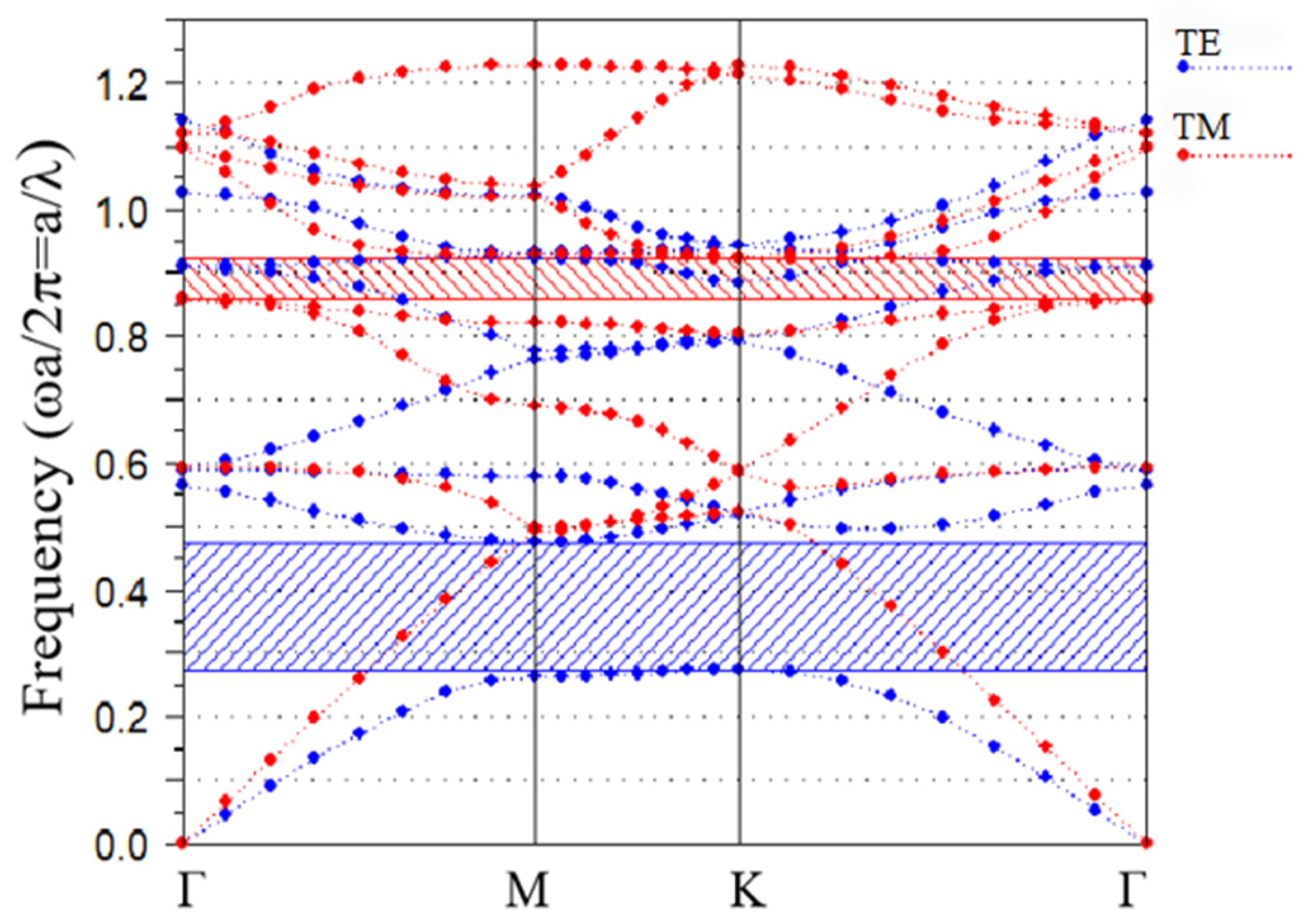
1. Introduction
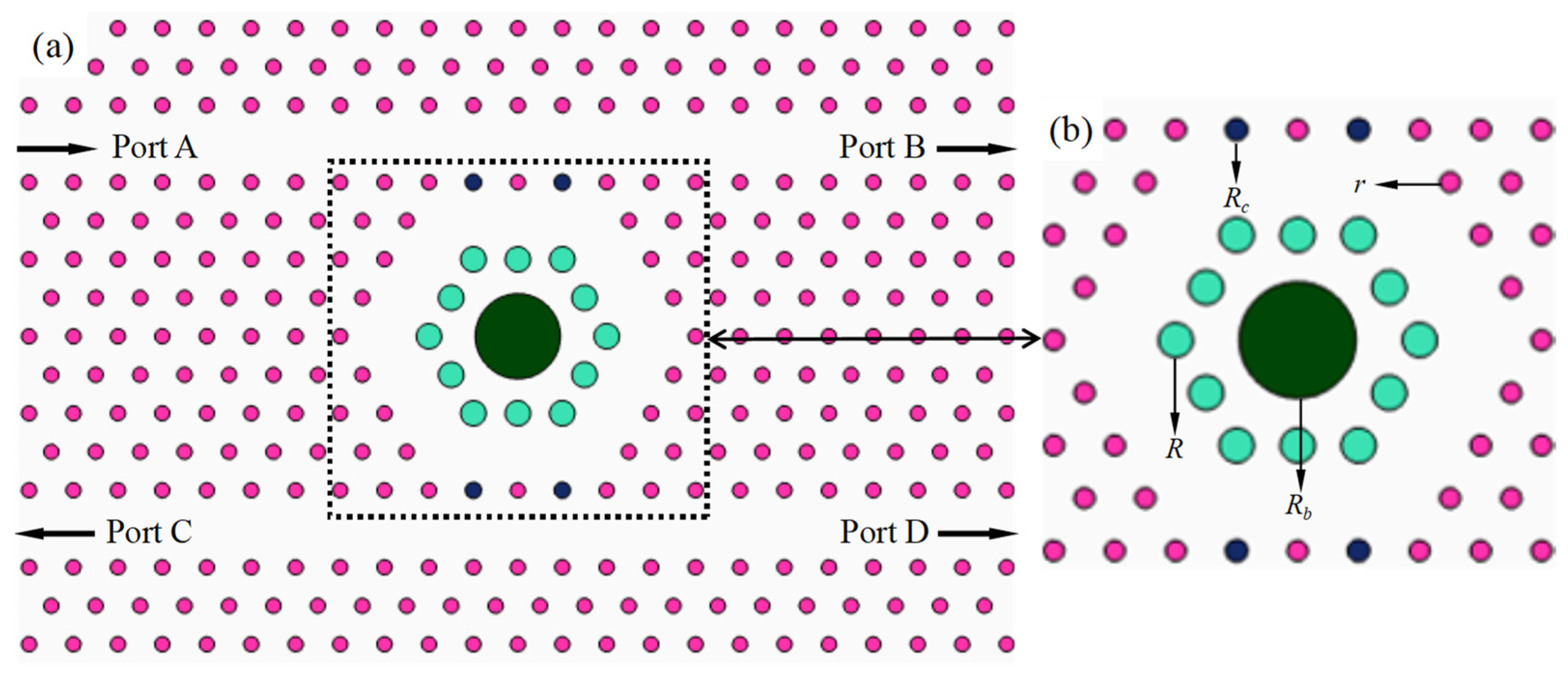
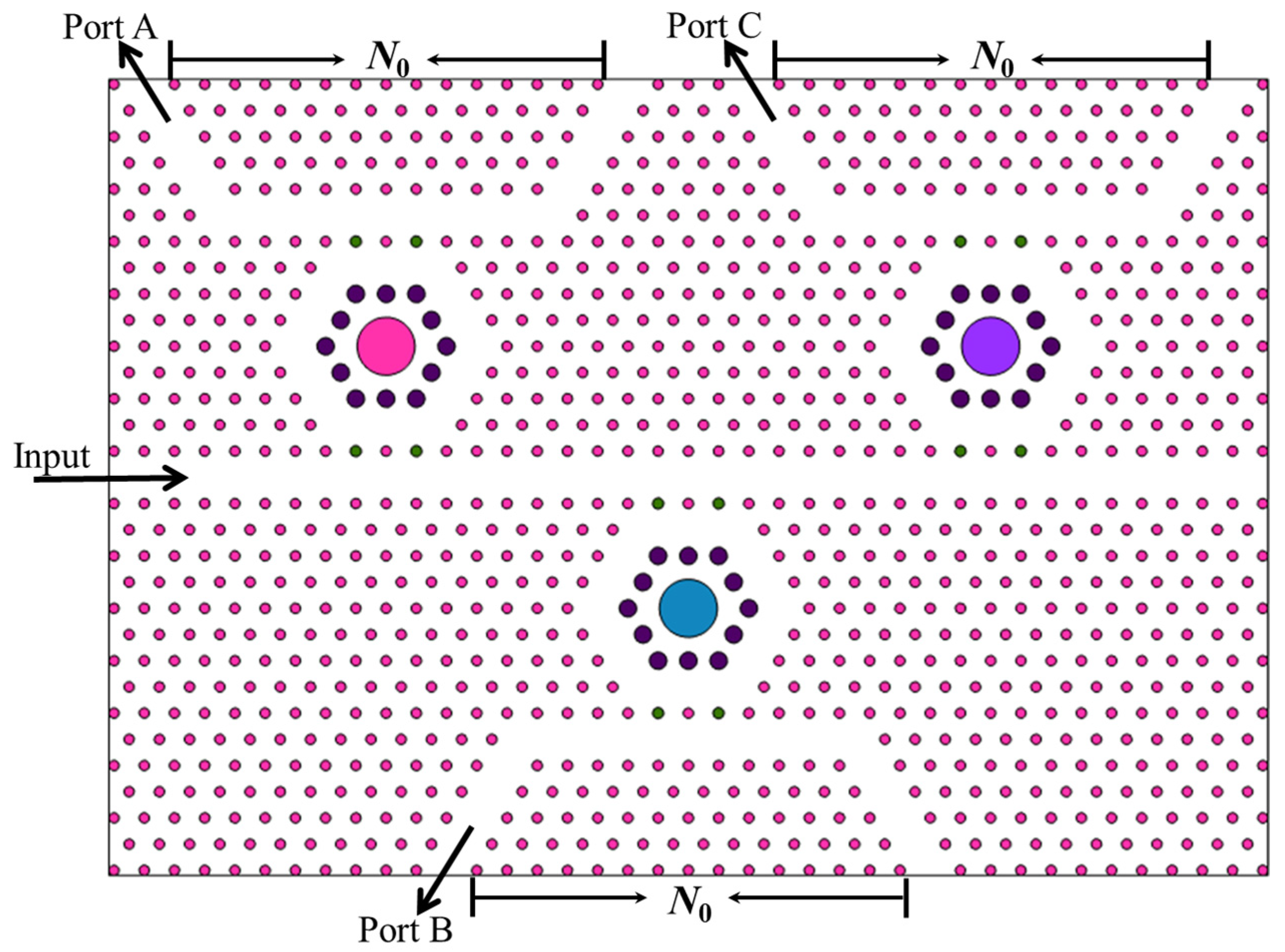
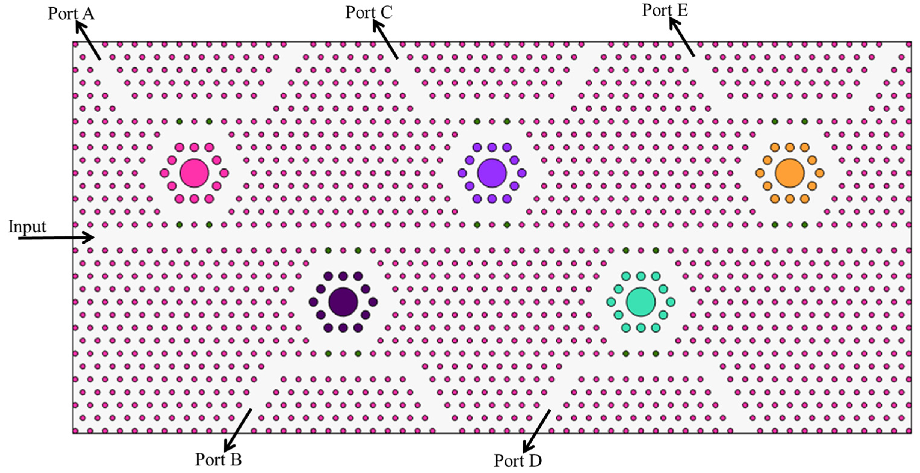
2. Description of the CDF Configuration
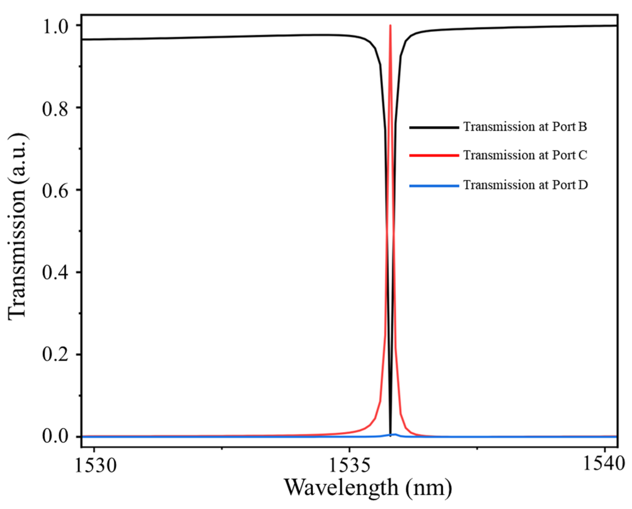
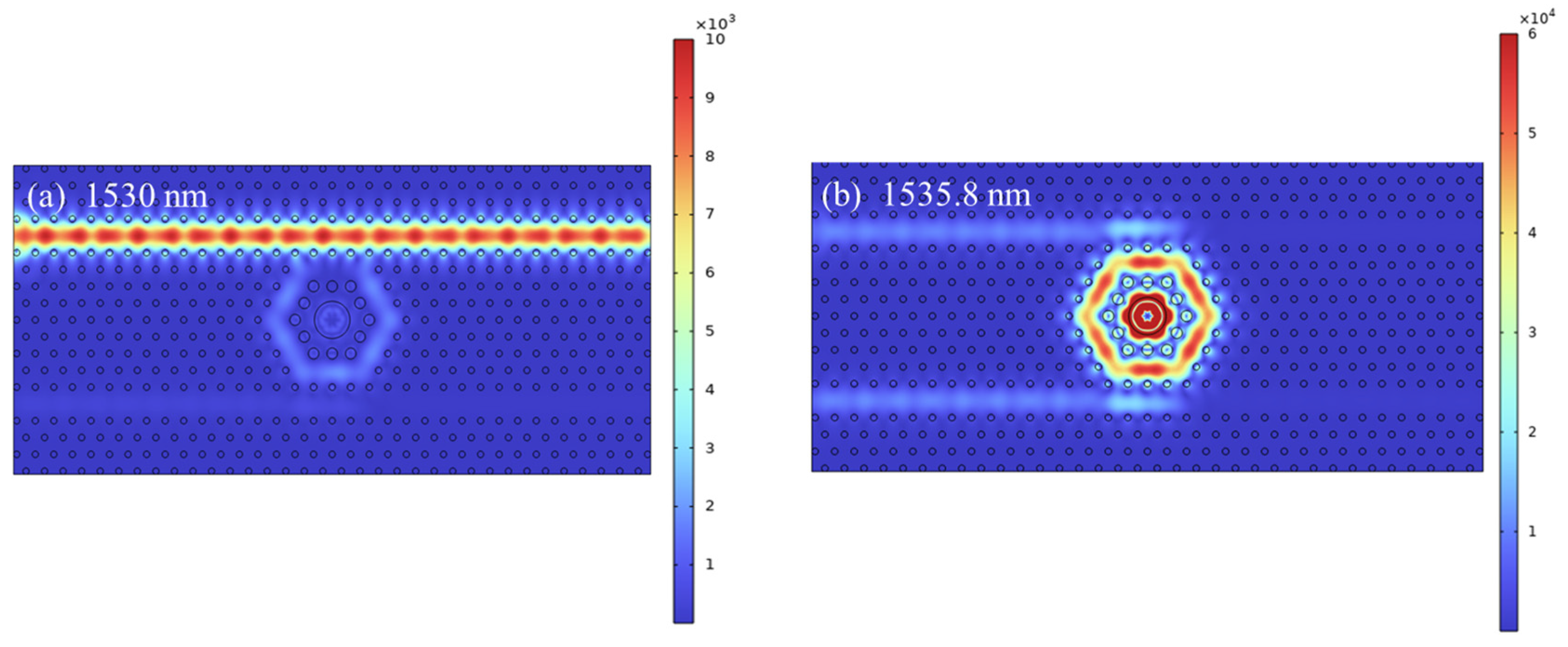
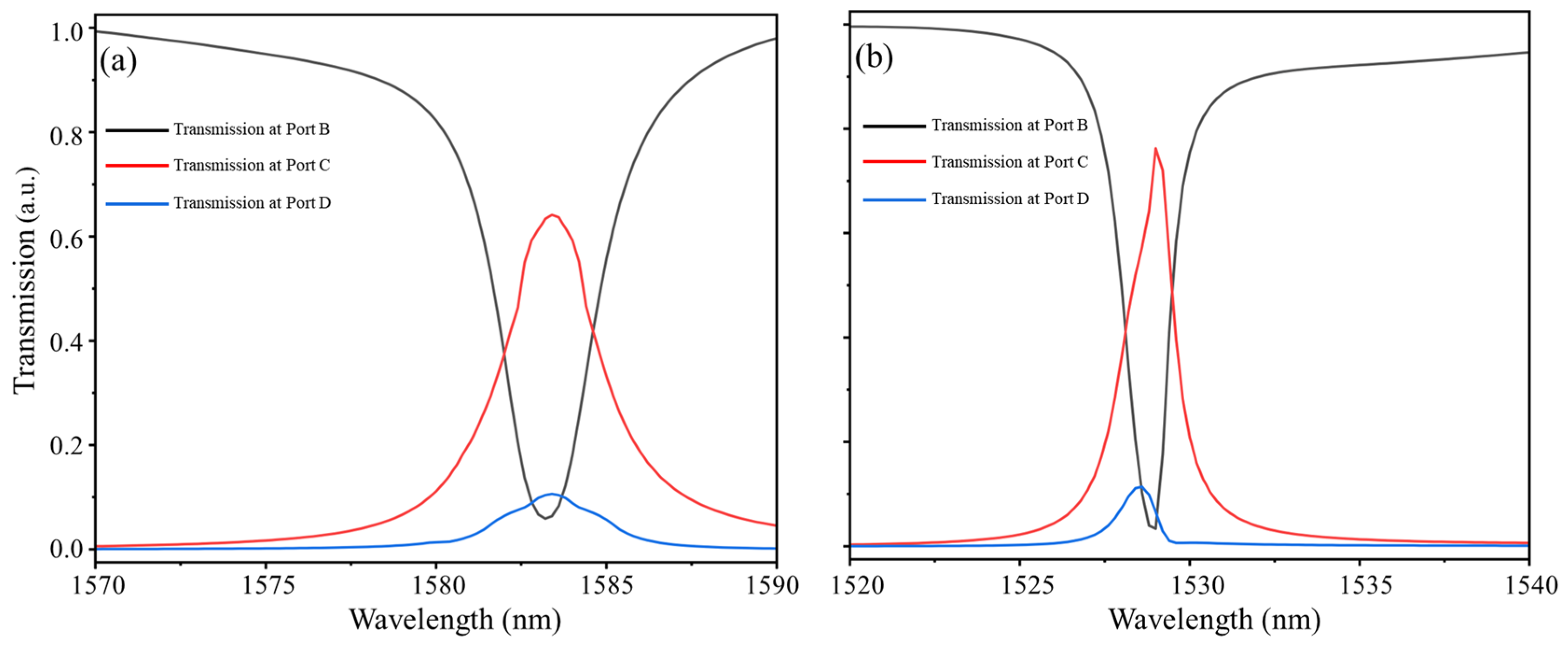
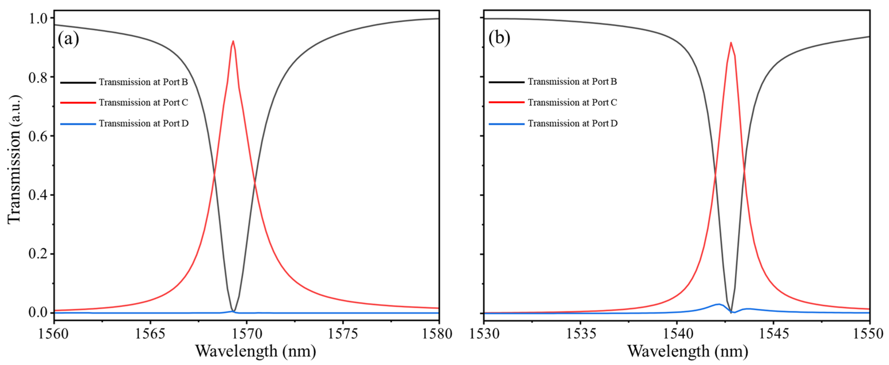
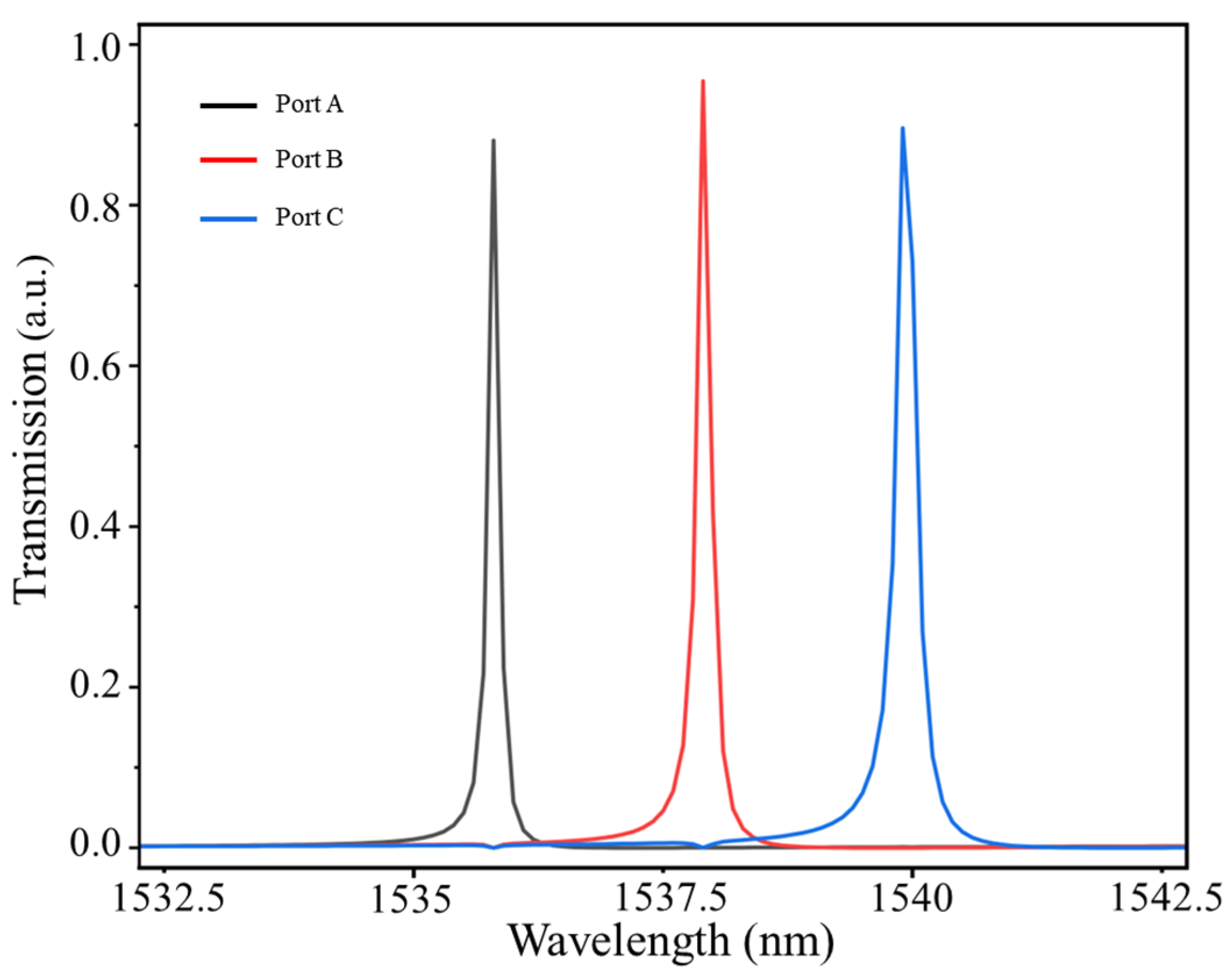
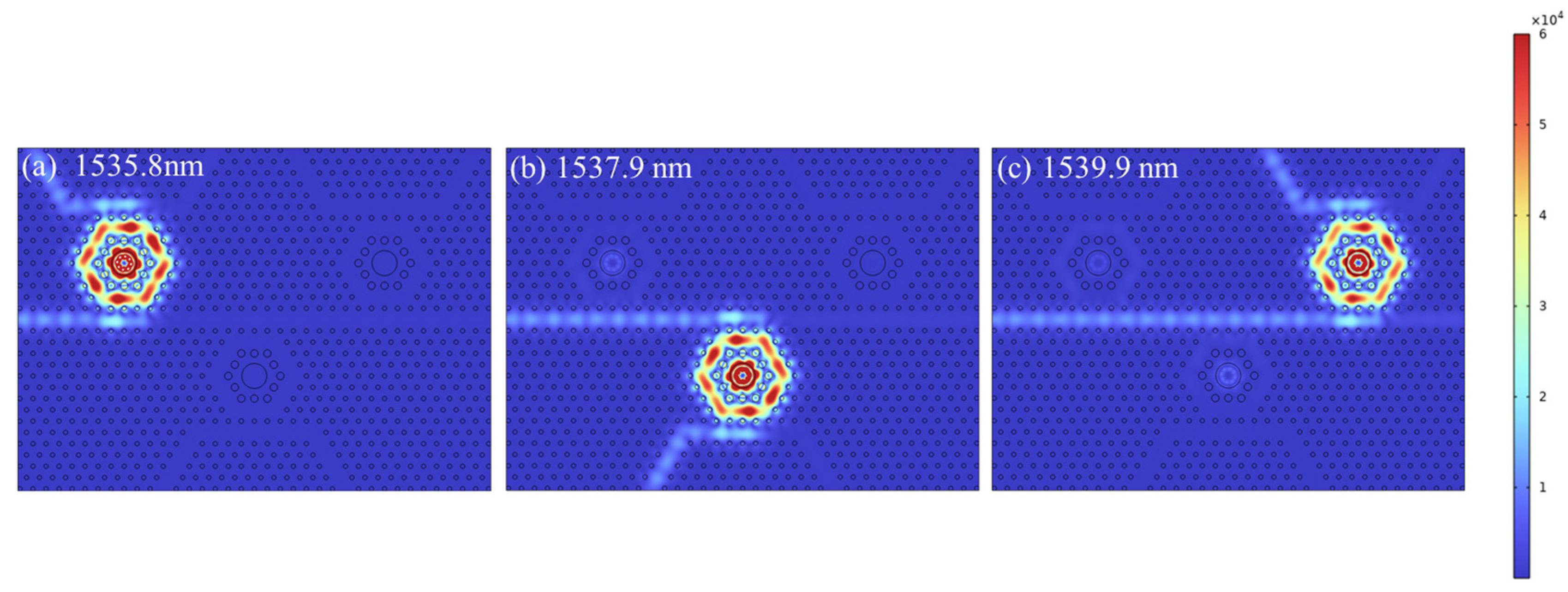
3. Description of the Optimal Three-Channel Filter
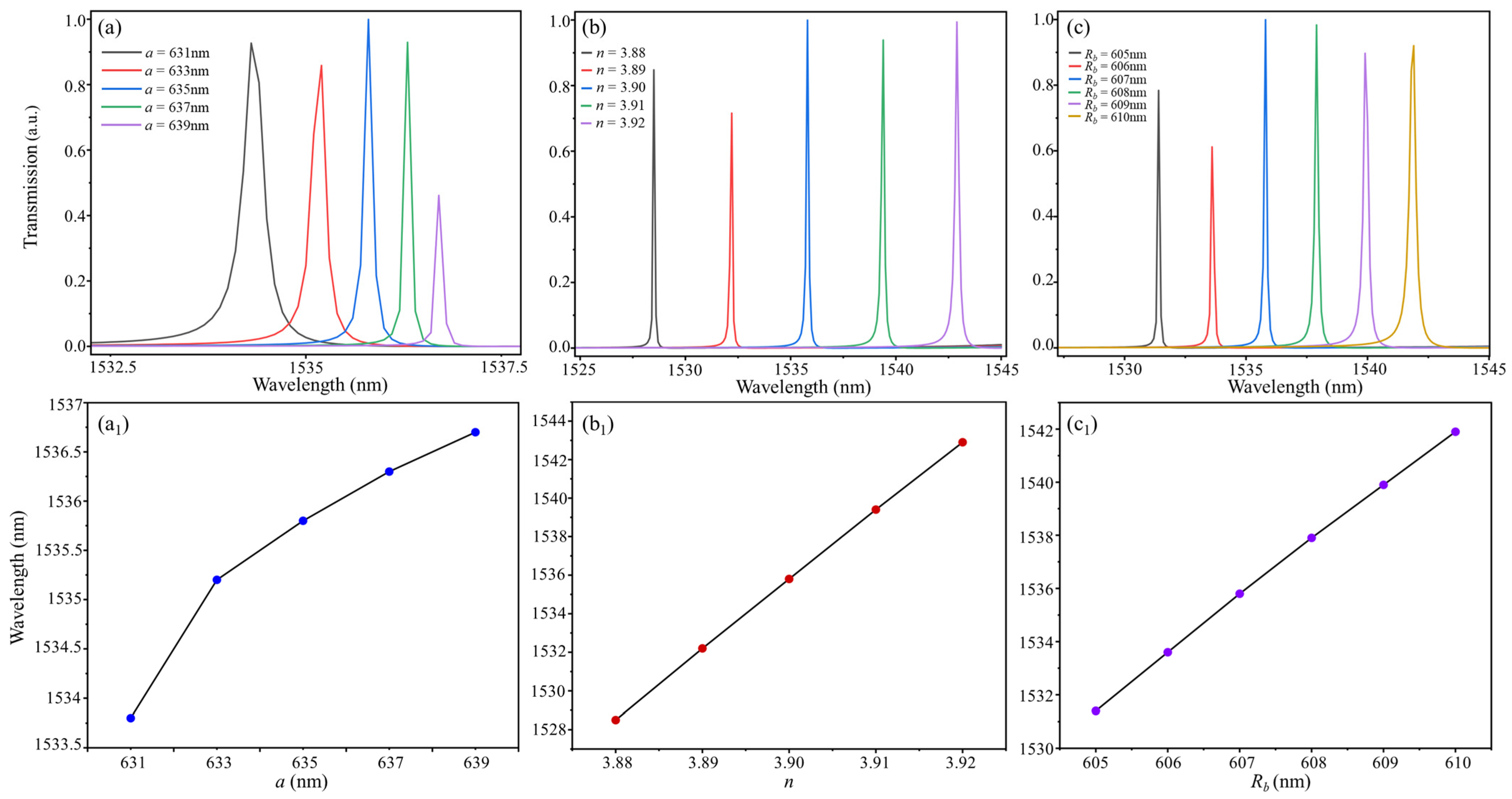
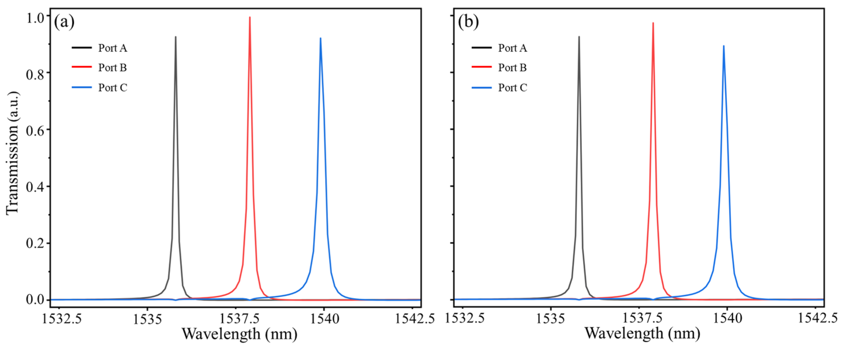
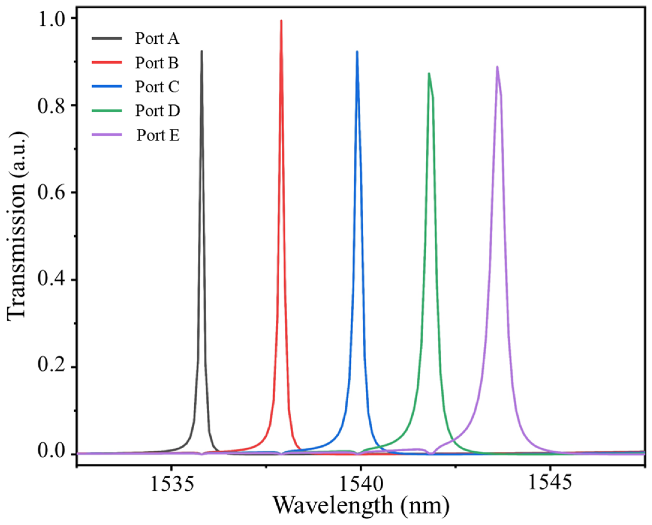
4. The Scalability Analysis
5. Conclusions
Author Contributions
Funding
Institutional Review Board Statement
Informed Consent Statement
Data Availability Statement
Conflicts of Interest
References
- Yablonovitch, E. Inhibited spontaneous emission in solid-state physics and electronics. Phys. Rev. Lett. 1987, 58, 2059–2062. [Google Scholar] [CrossRef]
- Plihal, M.; Maradudin, A.A. Photonic band structure of two-dimensional systems: The triangular lattice. Phys. Rev. B 1991, 44, 8565–8571. [Google Scholar] [CrossRef] [PubMed]
- John, S. Strong localization of photons in certain disordered dielectric superlattices. Phys. Rev. Lett. 1987, 58, 2486–2489. [Google Scholar] [CrossRef] [PubMed]
- Su, J.-Y.; Huang, X.-Q.; Xu, H.-L.; Zhou, J.-Y.; Meng, Z.-M. Ultrafast all-optical switching in a silicon-polymer compound slotted photonic crystal nanobeam cavity. Opt. Rev. 2023, 30, 33–40. [Google Scholar] [CrossRef]
- Gupta, P.K.; Paltani, P.P.; Tripathi, S. Pressure sensor based on two-dimensional photonic crystal ring resonator. Phys. Scr. 2023, 98, 125522. [Google Scholar] [CrossRef]
- Ghadrdan, M.; Mansouri-Birjandi, M.A. Concurrent implementation of all-optical half-adder and AND & XOR logic gates based on nonlinear photonic crystal. Opt. Quantum Electron. 2013, 45, 1027–1036. [Google Scholar]
- Al-Hawary, S.I.S.; Alkhayyat, A.; Shafieezadeh, M.M.; Dwijendra, N.K.A.; Khalaf, E.; Muda, I. A novel microstructure of 2-bit optical analog to digital converter based on kerr effect nonlinear nanocavities in 2D photonic crystal. J. Sens. 2023, 2023, 5795945. [Google Scholar] [CrossRef]
- Jervakani, A.T.; Darki, B.S. An ultracompact optical polarizer based on the one-dimensional photonic crystals containing anisotropic layers. Opt. Commmun. 2023, 526, 128884. [Google Scholar] [CrossRef]
- Wu, F.; Chen, M.; Xiao, S. Wide-angle polarization selectivity based on anomalous defect mode in photonic crystal containing hyperbolic metamaterials. Opt. Lett. 2022, 47, 2153–2156. [Google Scholar] [CrossRef]
- She, Y.; Liu, D.; Li, J.; Yao, M.; Zheng, Y.; Wu, F. Tunable wide-angle high-efficiency polarization selectivity based on a one-dimensional photonic crystal containing elliptical metamaterials. Phys. Lett. A 2024, 494, 129299. [Google Scholar] [CrossRef]
- Alagappan, G.; Wu, P. Design of sharp transmission filters using band-edge resonances in one-dimensional photonic crystal hetero-structures. Appl. Phys. B 2009, 96, 709–713. [Google Scholar] [CrossRef]
- Li, L.; Liu, G.Q. Photonic crystal ring resonator channel drop filter. Opt. Int. J. Light Electron Opt. 2013, 124, 2966–2968. [Google Scholar] [CrossRef]
- Kang, M.; Jin, H.; Jeon, H. Photonic crystal L3 cavity laser fabricated using maskless digital photolithography. Nanophotonics 2022, 11, 2283–2291. [Google Scholar] [CrossRef]
- Geiss, R.; Diziain, S.; Steinert, M.; Schrempel, F.; Kley, E.; Tünnermann, A.; Pertsch, T. Photonic crystals in lithium niobate by combining focussed ion beam writing and ion-beam enhanced etching. Phys. Status Solidi A 2014, 211, 2421–2425. [Google Scholar] [CrossRef]
- Saha, N.; Brunetti, G.; di Toma, A.; Armenise, M.N.; Ciminelli, C. Silicon Photonic Filters: A Pathway from Basics to Applications. Adv. Photonics Res. 2024, 2024, 2300343. [Google Scholar] [CrossRef]
- Liu, K.; Jin, N.; Cheng, H.; Chauhan, N.; Puckett, M.W.; Nelson, K.D.; Behunin, R.O.; Rakich, P.T.; Blumenthal, D.J. Ultralow 0.034 dB/m loss wafer-scale integrated photonics realizing 720 million Q and 380 μW threshold Brillouin lasing. Opt. Lett. 2022, 47, 1855–1858. [Google Scholar] [CrossRef]
- Saha, N.; Brunetti, G.; Armenise, M.N.; Ciminelli, C. Tunable narrow band add-drop filter design based on apodized long period waveguide grating assisted co-directional coupler. Opt. Express 2022, 30, 28632–28646. [Google Scholar] [CrossRef] [PubMed]
- Zhu, T.; Hu, Y.; Gatkine, P.; Veilleux, S.; Bland-Hawthorn, J.; Dagenais, M. Arbitrary on-chip optical filter using complex waveguide Bragg gratings. Appl. Phys. Lett. 2016, 108, 101104. [Google Scholar] [CrossRef]
- Gatkine, P.; Veilleux, S.; Hu, Y.; Bland-Hawthorn, J.; Dagenais, M. Arrayed waveguide grating spectrometers for astronomical applications: New results. Opt. Express 2017, 25, 17918–17935. [Google Scholar] [CrossRef]
- Takada, K.; Abe, M.; Shibata, T.; Okamoto, K. 10-GHz-spaced 1010-channel tandem AWG filter consisting of one primary and ten secondary AWGs. IEEE Photonic Technol. Lett. 2001, 13, 577–578. [Google Scholar] [CrossRef]
- Dai, D.; He, S. Highly sensitive sensor based on an ultra-high-Q Mach-Zehnder interferometer-coupled microring. J. Opt. Soc. Am. B 2009, 26, 511–516. [Google Scholar] [CrossRef]
- Chergui, I.; Bounaas, F.; Labbani, A. Novel design of four-channel wavelength division demultiplexer based on two-dimensional photonic crystal ring resonators. In Proceedings of the 2022 International Conference of Advanced Technology in Electronic and Electrical Engineering (ICATEEE), M’sila, Algeria, 26–27 November 2022; pp. 1–4. [Google Scholar]
- Dhandrapati, L.; Tupakula, S. A novel 8-channel DWDM demultiplexer on silicon photonic crystal slab: Design and analysis. Optik 2022, 256, 168734. [Google Scholar] [CrossRef]
- Al Dujaili, M.J.; Abed, N.H. Design a Photonic Crystal Narrowband Band Pass Filter at a Wavelength of 1570 nm for Fiber Optic Communication Applications. Wirel. Pers. Commun. 2023, 131, 877–886. [Google Scholar] [CrossRef]
- Chanu, S.A.; Sonkar, R.K. High coupling efficiency photonic crystal waveguide for compact channel drop filter design on silicon-on-insulator platform. Opt. Eng. 2023, 62, 087101. [Google Scholar] [CrossRef]
- Olivier, S.; Benisty, H.; Weisbuch, C.; Smith, C.J.M.; Krauss, T.F.; Houdré, R. Coupled-mode theory and propagation losses in photonic crystal waveguides. Opt. Express 2003, 11, 1490–1496. [Google Scholar] [CrossRef] [PubMed]
- Adachi, S. Optical dispersion relations for GaP, GaAs, GaSb, InP, InAs, InSb, AlxGa1−xAs, and In1−xGaxAsyP1−y. J. Appl. Phys. 1989, 66, 6030–6040. [Google Scholar] [CrossRef]
- Guo, S.; Albin, S. Simple plane wave implementation for photonic crystal calculations. Opt. Express 2003, 11, 167–175. [Google Scholar] [CrossRef]


| Parameter | Illustration | Value |
|---|---|---|
| a | Lattice constant | 635 nm |
| n | Common dielectric rods refractive index | 3.9 |
| n0 | Air refractive index | 1 |
| r | Common dielectric rods radius | 106 nm |
| R | Intracavity light-green dielectric rods radius | 180 nm |
| Rb | Intracavity dark-green large dielectric rods radius | 607 nm |
| Rc | Scattering dielectric rods radius | 115 nm |
| Xij (dB) | Port A | Port B | Port C |
| Port A | —— | −48.80 | −50.61 |
| Port B | −38.10 | —— | −40.28 |
| Port C | −30.16 | −45.71 | —— |
| Ref. | Cavity Shape | Transmittance (%) | Q Factor | Average Transmittance (%) | Average Q Factor |
|---|---|---|---|---|---|
| [22] | Octagonal ring cavity | 99.9 | 3883.2 | 99.45 | 1613 (four-channel) |
| [23] | Regular hexagonal ring cavity | 50 | 5000 | 70.4 | 5150 (eight-channel) |
| [24] | Nested circular ring cavity | 97.4 | 4268 | —— | —— |
| [25] | Line defect cavity | —— | —— | 88.0 | 4783 (three-channel) |
| Proposed | A dielectric column with large radius inside hexagonal ring resonator | 99.7 | 12,798.4 | 94.6 | 10,617 (three-channel) |
Disclaimer/Publisher’s Note: The statements, opinions and data contained in all publications are solely those of the individual author(s) and contributor(s) and not of MDPI and/or the editor(s). MDPI and/or the editor(s) disclaim responsibility for any injury to people or property resulting from any ideas, methods, instructions or products referred to in the content. |
© 2024 by the authors. Licensee MDPI, Basel, Switzerland. This article is an open access article distributed under the terms and conditions of the Creative Commons Attribution (CC BY) license (https://creativecommons.org/licenses/by/4.0/).
Share and Cite
Zhang, A.; Yang, X.; Wang, J. Design of Channel Drop Filters Based on Photonic Crystal with a Dielectric Column with Large Radius inside Ring Resonator. Photonics 2024, 11, 554. https://doi.org/10.3390/photonics11060554
Zhang A, Yang X, Wang J. Design of Channel Drop Filters Based on Photonic Crystal with a Dielectric Column with Large Radius inside Ring Resonator. Photonics. 2024; 11(6):554. https://doi.org/10.3390/photonics11060554
Chicago/Turabian StyleZhang, Ailing, Xiangyu Yang, and Junfeng Wang. 2024. "Design of Channel Drop Filters Based on Photonic Crystal with a Dielectric Column with Large Radius inside Ring Resonator" Photonics 11, no. 6: 554. https://doi.org/10.3390/photonics11060554
APA StyleZhang, A., Yang, X., & Wang, J. (2024). Design of Channel Drop Filters Based on Photonic Crystal with a Dielectric Column with Large Radius inside Ring Resonator. Photonics, 11(6), 554. https://doi.org/10.3390/photonics11060554