Article

Laser Machining at High ∼PW/cm2 Intensity and High Throughput

by
Nan Zheng
1,†,
Ričardas Buividas
1,2,*,†,
Hsin-Hui Huang
1,*,
Dominyka Stonytė
3,
Suresh Palanisamy
4,
Tomas Katkus
1,
Maciej Kretkowski
5,
Paul R. Stoddart
6 and
Saulius Juodkazis
1,3,7
1
Optical Sciences Centre, ARC Training Centre in Surface Engineering for Advanced Materials (SEAM), Swinburne University of Technology, Hawthorn, VIC 3122, Australia
2
Quoba Systems Pty. Ltd., 26-28 Roberna St., Moorabbin, VIC 3189, Australia
3
Laser Research Center, Physics Faculty, Vilnius University, Saulėtekio Ave. 10, 10223 Vilnius, Lithuania
4
Department of Mechanical Engineering and Product Design Engineering, Swinburne University of Technology, Hawthorn, VIC 3122, Australia
5
Research Institute of Green Science and Technology, Shizuoka University, Hamamatsu Campus, Hamamatsu 432-8011, Japan
6
Department of Engineering Technologies, Swinburne University of Technology, Hawthorn, VIC 3122, Australia
7
WRH Program, International Research Frontiers Initiative (IRFI), Tokyo Institute of Technology, Nagatsuta-cho, Midori-ku, Yokohama 226-8503, Japan
*
Authors to whom correspondence should be addressed.
These authors contributed equally to this work.
Photonics 2024, 11(7), 598; https://doi.org/10.3390/photonics11070598
Submission received: 2 June 2024 / Revised: 21 June 2024 / Accepted: 22 June 2024 / Published: 26 June 2024
(This article belongs to the Special Issue Advanced Photonic Sensing and Measurement II)

Abstract

:
Laser machining by ultra-short (sub-ps) pulses at high intensity offers high precision, high throughput in terms of area or volume per unit time, and flexibility to adapt processing protocols to different materials on the same workpiece. Here, we consider the challenge of optimization for high throughput: how to use the maximum available laser power and larger focal spots for larger ablation volumes by implementing a fast scan. This implies the use of high-intensity pulses approaching ∼PW/cm2 at the threshold where tunneling ionization starts to contribute to overall ionization. A custom laser micromachining setup was developed and built to enable high speed, large-area processing, and easy system reconfiguration for different tasks. The main components include the laser, stages, scanners, control system, and software. Machining of metals such as Cu, Al, or stainless steel and fused silica surfaces at high fluence and high exposure doses at high scan speeds up to 3 m/s were tested for the fluence scaling of ablation volume, which was found to be linear. The largest material removal rate was 10 mm3/min for Cu and 20 mm3/min for Al at the maximum power 80 W (25 J/cm2 per pulse). Modified surfaces are color-classified for their appearance, which is dependent on surface roughness and chemical modification. Such color-coding can be used as a feedback parameter for industrial process control.

1. Introduction

Tools have defined technical advancement throughout human history. They should provide the required virtues for particular tasks and very often for material processing, where they should have high resolution and high throughput of area or volume processing. However, resolution and throughput are usually considered a trade-off [1], which is known as Tennant’s law in the fields of optical and related lithographies [2] and ultrafast laser processing [3]. It becomes an optimization task to simultaneously achieve a specific resolution required for an application and to enhance throughput, usually through power scaling of the writing source (laser, electron beam, or ion beam). In optical lithography for microelectronic applications, high throughput was achieved via large-area projection systems [4,5,6,7], while resolution was gained by using shorter wavelengths [8,9,10,11]. However, these large-area processing tools are naturally losing flexibility to be adapted for different processes and are increasingly expensive due to the requirement for highly uniform exposure conditions over larger areas. Also, the multi-step fabrication processes in microelectronics create an additional challenge for overall throughput.
The recent decade of advances in 3D printing has stemmed from flexibility, on-demand fabrication, and prototyping capabilities which are well aligned with the relatively small footprint of tools/printers and low ownership and maintenance costs. One common virtue of 3D printing approaches based on the use of light, fluidics, moulding, embossing, etc., is the direct writing approach. While this sacrifices the productivity gains of large-area projection tools, it benefits from the ability to deliver the required exposure dose of energy/material for building a workpiece with tailored properties on the surface and inside the volume. When the depth of energy deposition becomes important for volume-per-time modification (rather than the saturation of thin-film "resist" exposure), laser machining is a very appealing approach [12].
Laser 3D processing of materials by the direct write approach is one of the most rapidly developing computer numerical control (CNC) machining methods, especially when ultra-short-pulsed lasers are used [13]. This leads to precise laser machining applications such as nano-scaled gratings [14,15] and nano-alloys [16]. A frontier science of high-energy research requires large-area patterned photo-electrodes for electron emitters and accelerators, which can be made using ablated ripple patterns [17] on Cu substrates [18]. Periodic patterns on Si can be used for a tunable visible-near-IR light source produced by free-electron bunch/beam and are compatable with CMOS technology [19]. Uniquely for sub-ps lasers, the pulse energy can be delivered and deposited faster than the material response: it takes ∼10 ps for energy transfer from the absorbing electronic sub-system of solid/liquid/gaseous phases to the atomic/molecular/ionic core sub-system. Subsequent hydrodynamic movement and phase transitions occur on time scales from tens-of-ps to microseconds. With a burst mode, where fs-pulses can be bunched into bursts with time separation corresponding to even higher MHz-GHz frequencies while keeping low frequencies of <MHz between the bursts, the fastest material removal rates ∼3 mm3/min become accessible and are comparable with mechanical CNC machining [20]. Similar arguments about using different energy deposition modes for high throughput modification of refractive index n in transparent materials predict that energy per volume is more effective than the power of exposure for a large change of n [21]. High-power 25 W laser machining of diamond for cutting tool applications was demonstrated using longer picosecond (355 nm/10 ps) pulses [22].
A particular aim of this study was to test the possibility of assembling the laser, stages, scanners, and 3D CNC machining software into a functional unit and to demonstrate the feasibility of laser ablation/patterning of large volumes/surfaces. Using the resulting setup, we apply high-pulse intensity/fluence per pulse [W/cm2 and J/cm2] with different total exposure doses up to 0.3 kJ/cm2 (per focal diameter) for laser machining of strongly reflective metals Al, Cu, and stainless steel based on a laser with 1030 nm wavelength and 200 fs pulses at a 0.1 MHz repetition rate when thermal accumulation is not dominant. The ablated volume reached significant removal rates V a 10 4   μ m3 at high beam travel speeds of ∼1 m/s and scaled linearly with the fluence per pulse, i.e., V a F p γ with γ 1 . The irradiance used for laser machining ∼0.2 PW/cm2 was approaching conditions where tunneling ionization becomes important (above 1 PW/cm2; see Appendix A). As compared with avalanche and multi-photon ionizations, which are dominant at 1–10 TW/cm2, tunneling ionization is of interest for more deterministic material machining due to the possibility of reaching higher precision, resolution, and polarization-controlled chemical bond breaking. The presented purpose-focused fs-laser machining setup can be assembled for a specific function and be acquired on a lower budget compared with commercial multi-functional fs-laser machining stations.

2. Experimental Section: Setup and Materials

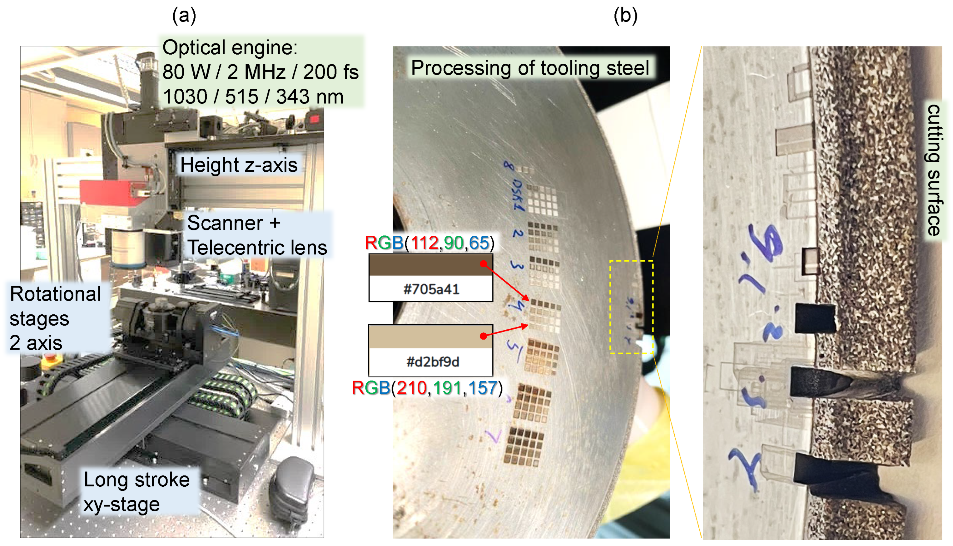
2.1. Assembly of fs-Laser Machining Setup

The multi-axis femtosecond laser CNC micro-machining system (Quoba Systems, Figure 1a) includes a high-power femtosecond laser, high-speed galvanometer scanner, 5-axis sample-positioning stages, system control, and software. The laser: 80 W Carbide (Light Conversion), wavelength of choice λ = 1030 , 515 , 343 nm, pulse duration t p = 200 fs, maximum pulse energy of 0.8 mJ, maximum repetition rate f = 2 MHz, and tunable GHz and MHz burst with burst-in-burst (bi-burst) capability. In burst mode, the output consists of pulse packets instead of single pulses, where each packet consists of a certain number of equally separated pulses. The MHz-burst contains up to 10 pulses with a 15 ns period and GHz-burst contains up to 10 pulses with a 440 ps period. Intra-burst amplitude slope can also be adjusted. Switching and adjusting bi-burst mode is fully automated. The Carbide laser comes with a fast energy control (FEC) capability, which allows changing the energy of each laser pulse at the MHz repetition rate. Switching between linear and circular polarization is also implemented across different wavelengths.
The telecentric fused-silica F-theta lens (Jenoptic, JENar, Jena, Germany) with F = 160 mm focal length was used with a galvanometer scanner (Raylase, SUPERSCAN IV, Weßling, Germany). The laser beam diameter D = 5 mm. This defines F-number F # = F / D = 32 and numerical aperture N A = 1 / ( 2 F # ) = 0.0156 . Theoretical diameter at focus 2 r = 4 λ π F # = 42 μ m. The depth of focus, D o F , = 8 λ π F # 2 = 2.69 mm for λ = 1030 nm; the axial extent of the pulse c t p = 60 μ m. With the most conservative estimate of the laser beam quality factor M 2 = 1.2 (measured value M 2 = 1.1 ), the beam diameter at focus becomes 50.5 μ m and D o F = 3.87 mm. Specifications of the F-theta lens focusing for the input beam at the conditions used give an estimate of 2 r = 60 μ m for the entire scanning field of 50 × 50 mm2. This was used for the calculation of fluence and intensity. Due to long D o F , multiple scans N s c = 1 10 were used to ablate deeper structures without a change in focusing depth. A change in scan direction was used between subsequent layers. Galvanometer scanners were equipped with dual-coating mirrors to accommodate for 1030 and 515 nm wavelengths.
High-precision, direct drive stages (Standa, Vilnius, Lithuania) with non-contact optical encoders ensure high positioning accuracy: 0.5 μ m bidirectional repeatability and 1 μ m absolute accuracy over the whole travel area of 400 × 400 mm. Maximum acceleration and speed are 2 g and 2 m/s, respectively. Stages were used for translating samples beyond the scanning field of the galvanometer scanner ( 50 × 50 mm in this case). The galvanometer scanner was mounted on a 200 mm travel Z stage with a high 20 kg vertical load capacity and similar positioning accuracy specifications as XY stages. System controllers (Polaris, Medina, MN, USA) were used to synchronize all axes with the laser, providing an infinite field of view (IFOV) capability, which splits motions task between stages and scanners, optimizing scanning speed and accuracy and eliminating stitching errors.
The system is controlled using a very capable and flexible software package (Direct Machining Control, DMC), which simplifies the laser machining design providing a user-friendly interface and ability to import various format fabrication tasks and also generate very complex machining paths without any G-code or other programming knowledge. DMC also integrates machine vision capability and provides automated galvo scanner field calibration.
The system is very modular and allows easy modifications to suit different fabrication requirements. Two high-precision rotational axes are available for a full 5-axis fabrication capability. Software and controllers are designed to control all 7 axes in real time and can accommodate up to 32 axes in total. The system also allows simple integration of high- N A objectives for high resolution (down to sub μ m) fabrication and Bessel beam setup integration for high-speed cutting of transparent materials. The presented modular structure of a versatile fs-laser machining setup can benefit from the latest developments in external pulse compressors (n2 Photonics GmbH, Hamburg, Germany), which are suitable for compression to 50 fs and 10 fs pulses in one or two stages, respectively, when high-peak-power fs-lasers are used; those compressors were not used in this study.

2.2. Ablation and Structural Characterization

Focusing and processing conditions were informed by the beam diameter on the surface 2 r = 60 μ m (nominal, without a telescope before F-theta lens) and twice as small with a beam expander, depth of focus D o F 2.7 mm (nominal), and scan speed for linear beam travel v s c = 100 1 mm/s (along x-direction), which defines the number of pulses per diameter from 60 to 6000 at f = 0.1 MHz (usual fabrication sequence was at a constant density of pulses per length of scan). Hatching between neighboring lines was chosen slightly smaller than the focal diameter and was Δ y = 50 μ m. The maximum fluence per pulse was F p = 28.3 J/cm2 and consequently average intensity I p = 0.14 PW/cm2.
A Geiger counter (Radhound with an SS315 probe) sensitive to hard X-rays above an energy level of 20 keV was used to monitor the emission of bremsstrahlung background. The background noise from the lab environment was 25 ± 5 counts per min (cpm). Shielding the direct view of the fabrication location on a workpiece with a sub-mm thick Al sheet was enough to reduce the X-ray counts back down to background level. RDS-32 monitor was used to determine radiation dose in μ Sv (∼20 cm from fabrication site) and was always at the background level for the highest power and pulse-to-pulse overlap (6000 pulses per diameter of 60 μ m).
Optical microscope (Nikon Optiphot-Pol., Tokyo, Japan) and profilometer (Bruker, Billerica, MA, USA) were used to image laser-machined regions and to determine the depth, which was evaluated with a precision of ∼0.1 μ m using high-numerical-aperture objective N A = 0.4–0.9 lenses.

2.3. Material Properties

Light–matter interaction is defined by the permittivity, which is the square of the complex refractive index ϵ 1 + i ϵ 2 ( n + i κ ) 2 = ( n 2 κ 2 ) + i 2 n κ of material at the wavelength of excitation (see Appendix B for another definition of the permittivity of metals). Herein, we collect material parameters relevant to the analysis (Section 3). Energy values for good metals: electron work function for Cu w e = 5.10 eV 100 orientation, 4.48 eV 110 , 4.94 eV 111 , and for Al 4.20; 4,06; 4.26 eV ( 100 ; 110 ; 111 ). For stainless steels, w e = 4.08–4.19 eV [23]. The refractive index at 1030 nm: n + i κ = 1.4033 + i 9.8532 (Al: absorption coefficient α = 1.2021 × 10 6 cm−1), 0.33769 + i 6.7731 (Cu: α = 8.2634 × 10 5 cm−1), n = 2.9421 + i 3.9094 and α = 4.7696 × 10 5 cm−1 for Fe (the main component of stainless steel).
The molar enthalpy of vaporization (and atomization) of Cu is 300 kJ/mol (338 kJ/mol) and similar values for Al 293 kJ/mol (326 kJ/mol). Solid density of Cu ρ C u = 8920 kg·m−3 (molar volume 7.11 cm3 and molar mass M C u = 63.546 g/mol) and that of Al ρ A l = 2700 kg·m−3 (molar volume M A l ρ A l = 10 cm3 where molar mass M A l = 26.98154 g/mol).

3. Framework for Analysis and Bench-Marking of Ablation Efficiency

Normalization of the ablation rate for the volume removal per pulse energy (for a photon) and the number of pulses (per pulse), e.g., μ m3/μJ/pulse, can be introduced to compare the ablation efficiencies of different fabrication methods and conditions.
The material removal for a dielectric by fs-laser was matched to the mechanical CNC machining rate in a burst mode for dental tissue ablation by ∼800 fs laser pulses [20] reaching V r = 5 × 10 7 μ m3/s (or ∼3 mm3/min) with N i b = 25 pulses (in a burst) of E p = 4 μ J/pulse energy at f i b = 1.7 GHz (in a burst), and separation between bursts was f b b = 1 kHz. At those conditions, good final quality of the ablated cavity was achieved via proper thermal management (no cracks were formed). The measure of ablation volume per single pulse is estimated as a removal rate per pulse and normalized to its energy as η p = V r / ( f b b N b E p ) [ μ m3/ μ J/pulse]. This estimate is still dependent on the in-a-burst frequency f i b . The η p was increasing for smaller E p when f i b is large in a nonlinear way due to thermal accumulation. For the burst removal of dental tissue, the efficiency per pulse was η p = 500 μ m3/ μ J/pulse. This example shows the ablation efficiency of a material of complex composition using single and burst modes of laser irradiation.
For industrial applications, the energy specific volume is introduced [24]: γ a = d V / d t P a v e = d V d E = s 2 d Δ t P a v e = d Δ x Δ y f r N s l P a v e [m3/J], where P a v e [W] is the average laser power, f r [Hz] is the laser repetition rate, Δ x = Δ y are the spot and line distances, respectively, s is the side length of the ablated square, d is its measured depth, and N s l is number of pulses (spot and line) per area of the side length s. The parameter γ a = d V d E [ μ m3/ μ J] defines the specific volume removal rate and has units of volume V per deposited energy E.

3.1. Energy Deposition Depth: Localization Mechanism

A common phenomenon of different ablation modes by ultra-short laser pulses with and without bursts is shallow energy deposition. It is responsible for the most efficient material removal rates in terms of volume per time and volume per photon. It is instructive to analyze energy deposition at the ablation threshold for metals (m) and dielectric (d) materials using the Gamaly model for the pulse fluence [25]:
F t h ( m ) = 3 8 ( ϵ b + w e ) λ n e 2 π , F t h ( d ) = 3 4 ( ϵ b + J i ) l s n e A ,
where ϵ b is the binding energy or enthalpy of vaporization, J i is the ionization potential, w e is the electron work function (escape energy from a metal), l s = c / ( ω κ ) λ / ( 2 π κ ) is the absorption depth (the skin depth) in the plasma with electron density n e and refractive index n = n + i κ with c and ω being the speed and cyclic frequency of light, respectively, and A is the absorption coefficient (for good metals A 2 ω l s c ). At high intensity, the pulse can exceed the ionization threshold and the first ionization is completed (before the end of the pulse), at which the number density of free electrons saturates at the level n e n a , where n a is the number density of atoms in the target material.
For ablation of dielectrics and semiconductors, which are ionized during the fs-pulse, a metal-like reflective plasma has A 0.5 ; i.e., half of the light is absorbed by the strongly excited material. The exact absorbed portion A = 1 R (where R is the reflection coefficient) can be precisely calculated from the refractive index n for the excited material as A = 4 n / [ ( n + 1 ) 2 + κ 2 ] . The most direct improvement of efficient (shallow) light energy deposition is achieved by the use of a shorter wavelength since l s λ . Interestingly, the ablation threshold of metals (Equation (1)) also scales with wavelength F t h ( m ) λ [25].
Equation (1) is based on the required energy budget to evaporate material ϵ b and to ionize it: w e for metals and J i for dielectrics. For metals, the electron work function enters the energy budget required to free electrons from the metal. The absorbed energy required for ablation is deposited into the skin depth l s of the excited material (dielectric or metal) with electron density n e and the portion of light absorption is defined by A ( A = 0.5 for the 50% absorbance). These ablation thresholds are confirmed by experiments for metals and dielectrics [25].

3.2. Ablation Rate

Given that T = 0 for the energy balance R + T + A = 1 , the theoretical limit of ablation rate per pulse is reached when the absorbed energy ( 1 R ) E p is equal to the enthalpy of vaporization ϵ b (binding, cohesive, atomization energy) in the volume where it is deposited. Since light absorption follows an exponentially decaying dependence via the Beer–Lambert law, shallow deposition into skin depth l s = 1 / α provides the most efficient material ablation. Such ablation is taking place by evaporation only as follows from the chosen energy balance. When ionization of material and plasma formation is taking place, the ablation requires a higher energy budget ( ϵ b + J i ) (Equation (1)).
The temperature of electrons in the skin depth is T e = ( 1 R ) F p / ( l s c e n 0 ) [25], where F p is the fluence per pulse, c e 3 / 2 is the electron specific heat, which acquires the value of 3/2 of the ideal gas after full ionization of material, and n 0 is the atomic number density of the material. This energy pool delivered to electrons acts as an energy reservoir for ablation after an ultra-short laser pulse, with T e reaching ∼2 keV in metal and silicon drilling [26], for example. The maximum material removed by a single pulse can be estimated from energy conservation [25]:
V m a x = ( 1 R ) E p / ( n 0 E a t / N a ) ,
where E a t [J/mol] is the molar enthalpy of atomization and N A the Avogadro constant.
While the practical ablation rates by vaporization in terms of removed volume V r [ μ m3/s] will not be the fastest, they are the most efficient in terms of deposited light energy. Kinetic factors are very important and are qualitatively discussed here for different ablation conditions.

3.3. Power Scaling of Direct Energy Deposition per Volume

Interestingly, the ablation efficiency of the burst ablation of dental tissue (dielectric) scales as η p E p 2 [20], while there is a linear dependence for single-pulse ablation and it extends over all tested pulse energy values for the case of direct absorption η p E p [12]. This difference can be explained by the density of absorbed energy, which scales as W a b s [ W / cm 3 ] = 2 A F p / l a b s n e n c r F p [25,27], where n e F p is the photo-excited electron density (which is also proportional to the fluence per pulse F p ), n c r = ϵ 0 m e e 2 ω 2 is the critical electron density where m e is the electron mass, e is the electron charge, ω = 2 π c / λ is the cyclic frequency of light, ϵ 0 is the permittivity of vacuum, and l a b s is the axial extent of energy deposition along the beam propagation direction ( n c r = 9.48 × 10 21 cm−3 at a 343 nm wavelength [12] and 1.04 × 10 21 cm−3 for 1035 nm, used in burst-ablation).
For the conditions where electron density n e < n c r , the absorbed energy density follows a nonlinear W a b s ( I p ) n e ( I p ) F p / n c r dependence on pulse intensity (irradiance) I p , while it becomes linear when the plasma reaches the critical density n e = n c r . For two-photon absorption in silica, the cavitation ablation rate followed the third power law γ = 3 [12]. Two-photon absorption corresponds to electron excitation n e I p 2 , and hence the absorbed energy density in the volume, which is proportional to the ablated volume, is W a b s F p 3 ; the pulse energy, fluence, and irradiance are all proportional to each other: E p F p I p . In the case of burst-ablation of dental tissue, the ablation rate was proportional to F p 2 [20], which can be explained by the linear absorption with n e I p . For metals, where absorption of the laser pulse is not increasing the electron density, which is close to n c r , a linear scaling with γ = 1 is expected and was confirmed in this study.

4. Results

We aimed to use the maximum available laser power of P = 80 W with pulse energy E p = 0.8 mJ per pulse at the repetition rate f = 0.1–1 MHz to maximize the use of the available light energy. The scan speed and focus were tuned for the required quality of the processed surface (smooth or rough) and the depth of ablated structures (hence removed volume V a mm3/min). Typical ablation thresholds are defined by the material properties (Equation (2)): for metals only 0.1 J/cm2 is needed [25] with pulses of λ 1 μ m and pulse duration t p = 200 fs; 0.2 J/cm2 is needed for silicon [28],; and ∼2 J/cm2 for wide-bandgap glass and crystals (fused silica and Al2O3) [25,29].

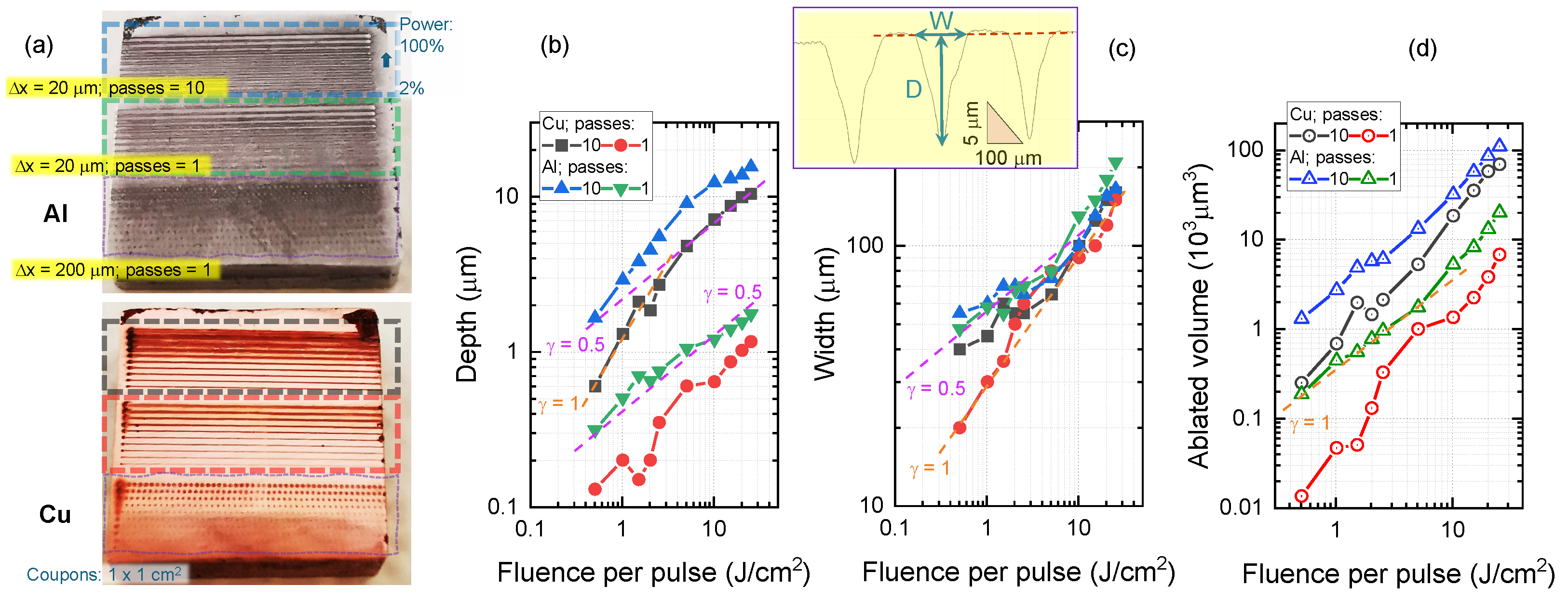
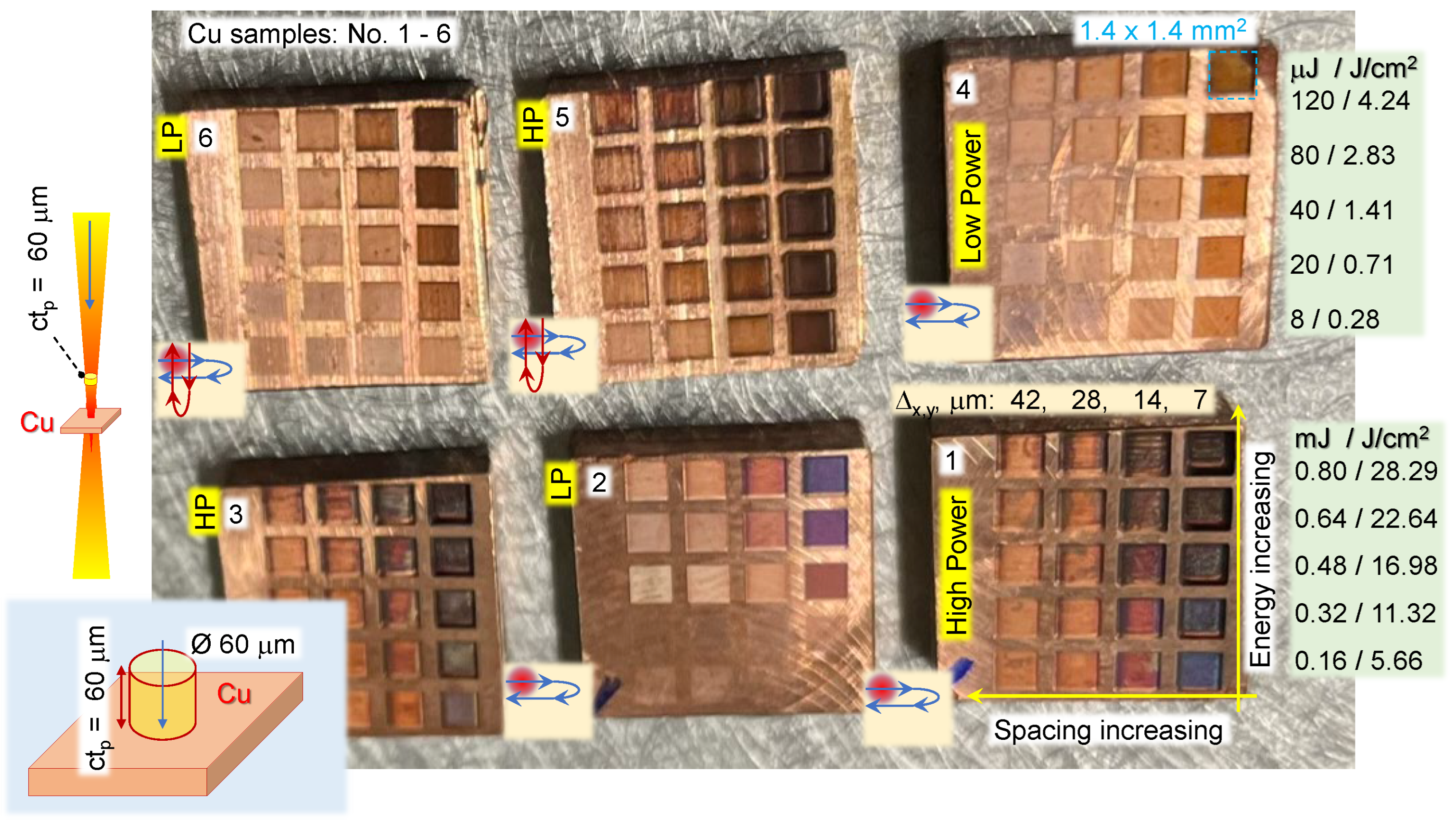
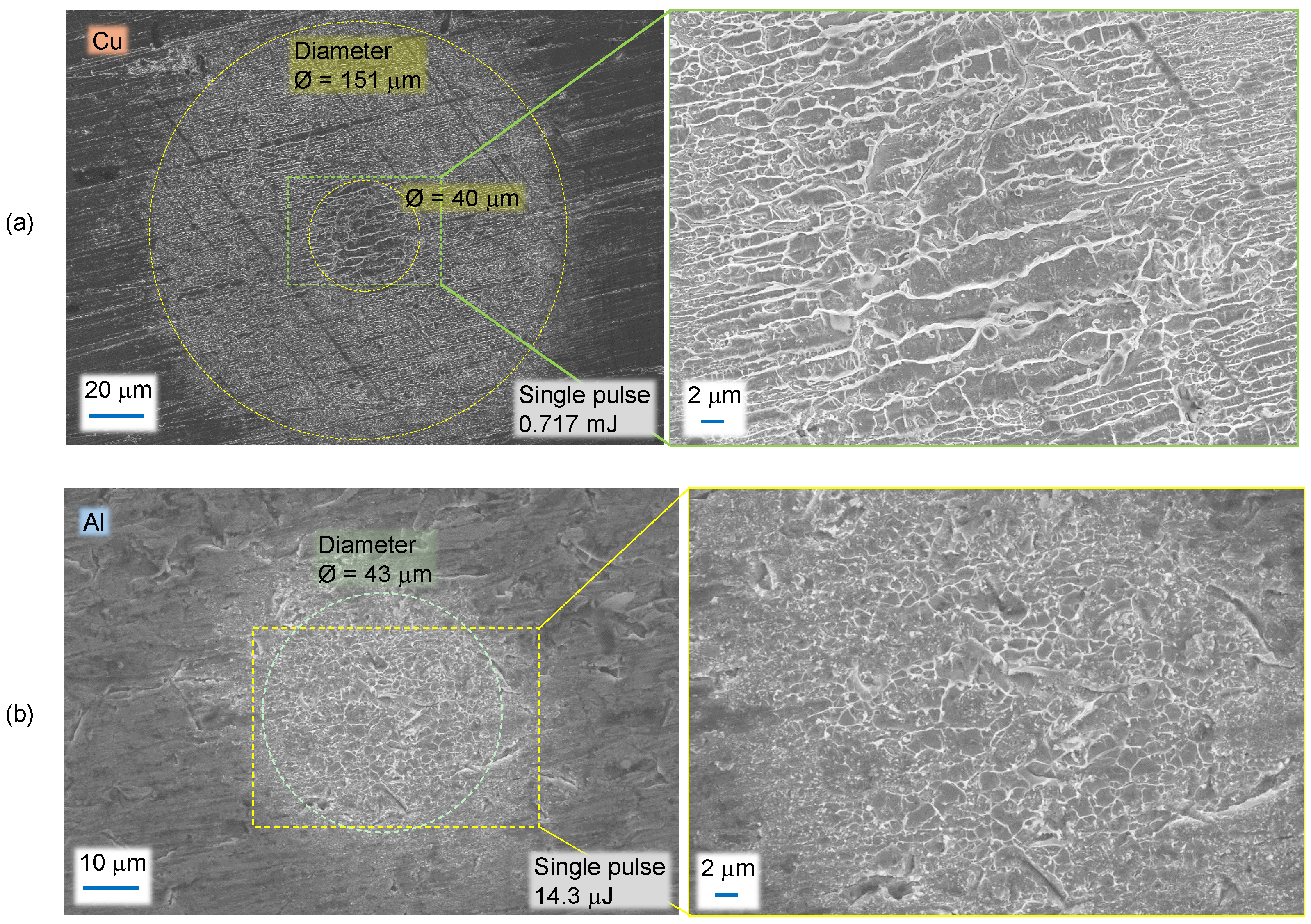
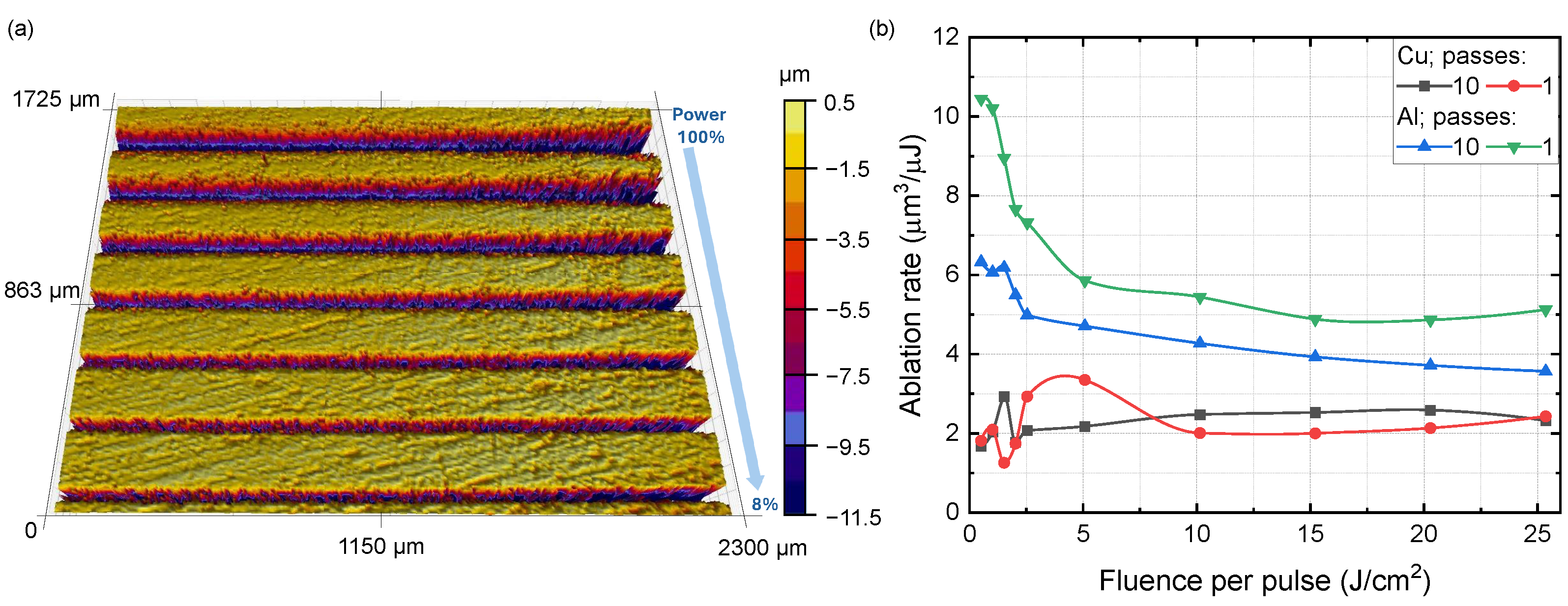
4.1. Cu and Al Ablation at High Scan Speed

Figure 2 shows typical samples of Cu which were ablated at an extensive range of conditions: from full power of 80 W corresponding to pulse energy E p = 800 μ J down to 16 μ J. The repetition rate was set to f = 0.1 MHz and the linear travel speed of the 60 μ m focal spot was v s c = 0.5 , 1 , 2 , 3 m/s, corresponding to pulse-to-pulse separations of Δ x , y 7 , 14 , 28 , 42 μ m; these are the measured separations determined from the ablation patterns and are slightly larger than expected from the set conditions due to very fast scan rates, which were the focus of this study. The same spacings were used in the x- and y-directions for the most uniform material removal. Surface coloration is caused by nano-micro-structure formation over the ablated regions, laser polishing at low fluence, and surface oxidation into CuO2 and CuO [30].
The depth, width, and volume ablated using single scans and scans repeated ten times are shown in Figure 3b–d, respectively. The log-log presentation reveals the scaling dependencies. The depth evolved as F p 0.5 , which indicates a heat diffusion process. A strong difference in depth for one and ten passes was observed. However, for the width, both single- and multi-pass structures converged and showed γ = 1 dependence. For the ablated volume, a close-to-linear dependence was observed for both Al and Cu. Since the critical density n c r for 1030 nm is smaller than the electron density in those metals n e , the linear scaling of ablated volume with fluence per pulse is expected. as shown above.
Figure 3. (a) Ablated lines at different pulse energies (powers) at 1 and 10 repeated passes on Cu and Al 1 × 1 cm2 coupons. Depth D (b) and width W (c) of the ablated line as a function of fluence per pulse; 1030 nm/200 fs/0.1 MHz at scanning speed corresponding to in-line separation between pulses Δ x = 20 μ m and 200 μ m (single-pulse regime Figure 4) and distance between lines 0.25 mm. Inset shows the cross-section from an optical profilometer. (d) Ablated volume of cone V = π D [ W / 2 ] 2 / 3 at different fluence per pulse (in terms of average power from 2% to 100%). The slopes of power dependencies D , W , V F p γ correspond to linear γ = 1 and diffusional γ = 0.5 .
Photonics 11 00598 g003
The specific ablation rates at different pulse energies and numbers of scans were dependent on the Cu and Al material properties, as summarized in Table 1. The ablation rate of copper increased from 1.81 to 2.43 μ m3/μJ for single-pass ablation and is a bit lower for 10 passes. The single-pass ablation efficiency of aluminum decreased with higher pulse energy from 10.44 to 5.13 μ m3/μJ, and from 6.33 to 3.57 μ m3/μJ for 10 passes. The tendency of γ a to reduce at large fluence for metals is common; here, 0.8 mJ pulses corresponded to an average fluence of 28.3 J/cm2, while for 16 μ J it was 5.7 J/cm2. The largest specific ablation rates γ a are observed at ∼1 J/cm2 in metals and are pulse-duration dependent. The largest material removal rate was 10.4 mm3/min for Cu and 22.1 mm3/min for Al at the maximum power 80 W (25 J/cm2 per pulse). Figure 5 shows ablation rates at a wider range of fluences.
It is noteworthy that for short pulses of ∼50 fs in dielectrics, γ a increases for lower fluences [24] due to the accumulation of optical defects during multi-pulse exposure causing a stronger ablation. Also, better edge quality and lower roughness are observed for ∼50 fs pulses, which are conveniently produced with an external cavity compressor module (MIKS1S, n2 Photonics GmbH, Hamburg, Germany) [24].
When the scanning speed was large enough to separate single pulses, SEM images revealed a nano-texture formation even for single pulses at low and high pulse fluence (Figure 4). The surface of the Al and Cu coupons had a micro-texture which was enhanced by ablation. This could contribute to lower reflectivity of the laser-treated regions and favor stronger energy deposition in subsequent passes. This tendency can be inferred from scaling γ > 1 in Figure 3.
Figure 4 shows typical single-pulse ablation sites on Al and Cu characterized by SEM. The surface of the coupons used in this work had micron-scale structures due to mechanical cutting. Those structures affected the light distribution and consequently the ablation. They are reminiscent of typical ablation ripples, which have a period (0.8–1) λ for absorbing samples under multi-pulse exposure. However, here they were produced by single-pulse exposure at high or low pulse energy. Interestingly, the affected region was larger than the directly exposed region ( I m a x / e 2 -level) for the highest pulse energy. Since the threshold of laser ablation fluence is only ∼0.1 J/cm2, low-intensity regions of the laser beam can already be delivering the required ablation fluence. The threshold of ablation is dependent on the energy distribution of the surface atoms, and it was shown to require time to be established; i.e., the high-energy side of the Maxwellian velocity distribution has to be established before evaporation from the surface can take place [31]. Ablation in a vacuum showed an approximately twice-higher ablation threshold [31] and is linked to slower thermalization when there is no ambient air. It would be useful to measure the ablation threshold at low pressure ∼ 10 3 bar (∼ 10 2 Pa) for the conditions used in this study, which was performed in ambient air.

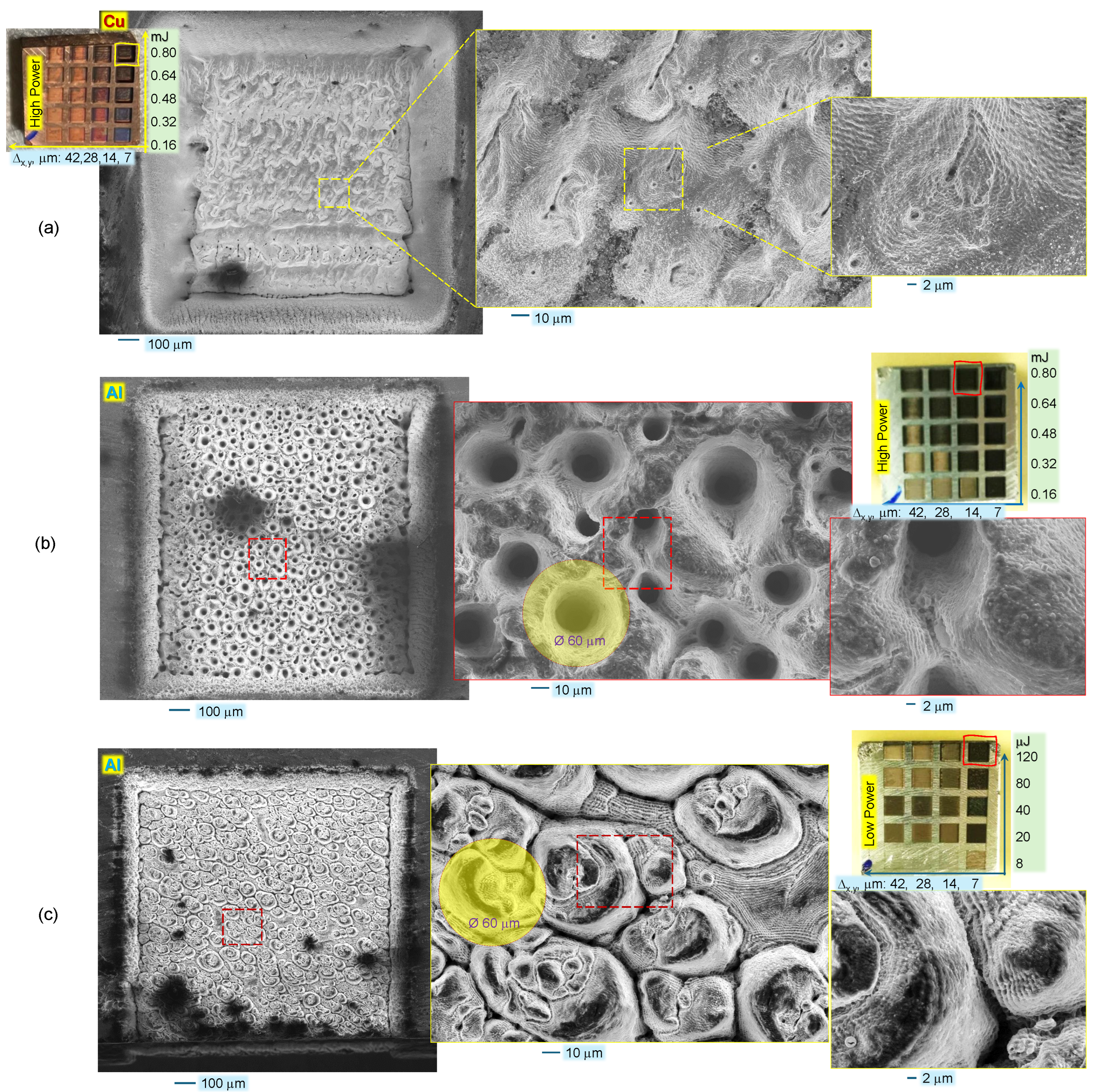
4.2. Silica Ablation and Defect Accumulation

The same high average power ablation as used for metals was applied to scan lines on fused silica (Figure 6). Analysis of ablation width vs. pulse fluence was carried out using the Liu method [32]. The single-pulse ( N = 1 ) ablation threshold for silica is F t h ( 1 ) = 2 J/cm2. For a linear scan with Δ x = 20 μ m translation steps between laser pulses, a smaller threshold was observed F t h ( N = 3 ) 0.8 J/cm2. This can be explained by the accumulation of defects, which causes increasingly stronger absorption for subsequent pulses. Phenomenologically, it is defined by the accumulation exponent γ a : F t h ( N ) = F t h ( 1 ) N γ a 1 , where γ a = 1 corresponds to absence of accumulation. Accumulation was present in the case of N 3 for silica. The slope of the w 2 F p dependence (Figure 6) changed approximately when the width of the ablated groove became larger than the focal diameter. In this case, the absorbed energy spreads by heat diffusion and is high enough to facilitate material removal by the ablation mechanisms of explosive boiling, evaporation, or ionization. The threshold for ablation at these conditions was ∼9 J/cm2, which is considerably larger than the single-pulse threshold of 2 J/cm2 typical for glasses [33]. The optical energy deposition and absorption scale is e 2 = 7.39 for intensity according to the Beer–Lambert law, which is usually applied to the depth profile of energy deposition in ablation studies [34].

4.3. X-ray Emission

X-ray emission was monitored and observed during laser fabrication with different pulse overlaps. In all cases, the same 100 kHz repetition rate, 200 fs pulse duration, and 0.8 mJ energy were used, with spot size 60 μ m and fluence 28 J/cm2. The X-ray emission was already six times above the background at 150 cpm (counts per minute) when the gap between pulses is at 1 μ m (60 pulse overlap per focal spot along the scan). The emission reached the highest level of ∼ 1.5 × 10 5 cpm when the gap between pulses was reduced to 0.1 μ m, i.e., an overlap of 600 pulses per focal spot. However, the emission drops down to ∼1850 cpm when the gap between pulses becomes even smaller at 0.01 μ m (overlap of 6 × 10 3 pulses per focal spot). This drop is related to a larger volume removed from the focal volume by ablation and the reduced amount of material affected, hence generating less bremsstrahlung radiation.

5. Discussion

It has been shown that a broad color gamut can be produced by fs-laser ablation of stainless steel using burst and bi-burst modes, resulting in intricate nanoscale patterns and structures [35]. Here, the color of the ablated matrices, which are typically used for optimization of two independent parameters of surface processing while keeping others constant, can be digitized into HEX codes (or RGB values), as shown in Figure 1b for two segments. Parametric information represented by color has the advantage of being both human- and machine-readable for purposes of automated process control. However, in an RGB color system, the color information is acquired in a device-dependent manner. Using cameras operating in RGB color space requires color calibration for the particular illumination conditions to obtain good color acquisition fidelity. Likewise, the reproduction of color on a display also has to be calibrated. Calibrated imaging systems can be very powerful and efficient in encoding various parameters, even more so in the trichromatic XYZ color space [36], which is device-independent and captures colors within the full vision gamut [37]. XYZ color space is much more accurate and can be also re-calculated (with loss) to RGB, sRGB, L*a*b* (lossless), and other high-fidelity color systems.
For the ablation matrices, the choice of the color acquisition instrument (camera vs. colorimeter) is dictated by the required precision of color identification. The color change that results from varying the ablation parameters can also be used for aesthetic and functional purposes. In the case of materials where coatings may not be desirable (like stainless steel or copper), a typical silkscreen layer used for marking the product can be replaced by ablation marks with colors of choice induced by chosen laser parameters. Conventional mechanical or laser engraving is very limited in that respect and usually requires additional setup in the production process. With femtosecond laser machining, the simplification of the processing setup may provide an advantage in production costs. Moreover, using materials that exhibit color change induced either electrically [38] or via mechanical stress [39] can open up a wide range of applications for laser-machined sensors/devices working on purely mechanical principles, such as low-energy consumption strain indicators, cutting tools with the level of wear indicated by color change, and many other applications. In addition to the above, recent developments in AI technology, coupled with increasing throughput, allow for five-axis laser machining to be introduced to the market with much more user-friendly software packages with learning curves much less steep than in conventional cutting [40,41]. With the non-contact approach to processing materials with lasers, thin-walled and fragile components can be manufactured with great precision at relatively low cost, which benefits many fields of applications, most notably single-use biomedical components, surgical tools, and healthcare equipment.
Colorimetric quantification of laser-processed areas on metals may have other applications for laser-processed regions inside the volume of transparent materials (Figure A2). In this case, laser-damaged regions show stress-induced birefringence for circularly polarized light. This polychromatic polarization microscope (PPM) imaging is promising for color analysis under white light illumination.
The black appearance of some ablated surfaces has another potential application in the IR spectral range. Such surfaces have high emissivity ϵ 1 according to the Kirchhoff law ϵ α = 1 R [42], where R is the reflectance, and such emissivity improvement has been demonstrated on aluminum [43], sapphire [44], and metal-on-insulator metasurfaces [45]. Metals are usually reflective but not emissive. The formation of black metal surfaces (see Al surfaces in the insets of Figure A1b,c) and their characterization in the IR-THz spectral range may support their use for radiative cooling in the 7–14 μ m spectral window of atmospheric transmission.

6. Conclusions and Outlook

Normalization to the number of pulses and pulse energy (number of photons) is a useful tool for comparing very different ablation modes with high-frequency bursts, as well as single pulses and with different pulse-overlapping modes during laser machining. The accumulation exponent of the ablation threshold is a useful parameter to assess the contribution of accumulation. The ablated volume of Al and Cu was found to scale linearly with pulse fluence at high-intensity conditions and the specific volume ablation rates of 2.43 μ m3/ μ J (Cu) and 5.13 μ m3/ μ J (Al) were achieved for a single pass at the full power of 80 W. As typical for metals closer to the threshold of ablation fluence < 1 J/cm2, the low melting point Al showed a higher ∼10.4 μ m3/ μ J removal rate at 80 W. This shows that there is always an optimization challenge for the most efficient use of photons for material removal. Lower roughness and sharper edges of ablated patterns are also obtained near threshold. The largest material removal rate was 10 mm3/min for Cu and 20 mm3/min for Al at the maximum power 80 W (25 J/cm2 per pulse).
The ablation thresholds are defined by fundamental material parameters such as binding energy, electron ionization potential and work function, and the skin depth electron density (original for metals and photo-excited for dielectrics), and they are dependent on the ambient pressure. The permittivity ε = n ˜ 2 of the material defines the energy deposition via the skin depth l s κ . This shows the importance of the energy per unit volume (J/cm3) in analyzing ablation and material removal for the defined fluence per pulse J/cm2. The absolute limit of material removal per pulse energy is based on energy conservation (Equation (2)).
Ablation of lower-melting-temperature metals such as Al showed micro-structures with feature sizes comparable with the dimensions of the focal spot. Black surfaces were formed on the usually reflective Al in the visible spectral range. Feature sizes of tens of micrometers make such surfaces anti-reflective and, hence, emissive at the longer IR-to-THz spectral range and will be investigated in a follow-up study. Laser-machined surfaces have a distinct color appearance at the visible spectral range. Color indexing can be used for in situ monitoring of laser-machined workpieces and may provide feedback for fully automated laser processing.

Author Contributions

Conceptualization, R.B., H.-H.H. and S.J.; methodology, R.B., H.-H.H., N.Z. and T.K.; software, R.B., M.K. and T.K.; validation, N.Z., D.S., S.P. and P.R.S.; formal analysis, N.Z. and R.B.; investigation, N.Z.; resources, P.R.S.; data curation, R.B. and N.Z.; writing—original draft preparation, S.J., N.Z. and H.-H.H.; writing—review and editing, all the authors; visualization, N.Z. and S.J.; supervision, R.B.; project administration, R.B.; funding acquisition, R.B. and P.R.S. All authors have read and agreed to the published version of the manuscript.

Funding

This research was partly funded by the Australian Research Council Linkage LP220100153 and Discovery DP240103231 grants.

Institutional Review Board Statement

Not applicable.

Informed Consent Statement

Not applicable.

Data Availability Statement

All the data are presented within this manuscript.

Acknowledgments

We acknowledge support by Swinburne University of Technology for lab allocation to test the 80 W fs-laser machining system. We are grateful for the demonstration of external pulse compression of Carbide fs-laser to 50 fs by Darius Gailevičius at the Laser Center, Vilnius University and for Jeremy Brown for X-ray and particles’ check.

Conflicts of Interest

The authors declare no conflicts of interest.

Appendix A. Tunneling Ionization

The atomic intensity I a = ε 0 c E a 2 / 2 = 3.51 × 10 16 W/cm2 corresponds to the electrical field strength E a = e 4 π ε 0 a B 2 = 5.1 × 10 9 V/m at the electron orbit of the Bohr radius a B = 2 m e e 2 = 0.53 Å in the hydrogen atom [46,47,48]. At laser intensity I L I a , tunneling ionization dominates. This condition is defined by the Keldysh parameter γ K ω L 2 E i o n / I L < 1 , where ω L is the cyclic frequency of laser and E i o n is the ionization potential. When the external electrical field of strength E e x is applied to an atom, the potential is given by V ( x ) = Z e 2 x e E e x x along the x direction. From the condition d V ( x ) d x = 0 , the position of barrier is x m a x = Z e / E e x , where Z is the atomic number (nuclear charge number). By setting V ( x m a x ) = E i o n , the critical (threshold) field strength for barrier suppression ionization (tunneling) is obtained E c = E i o n 2 4 Z e 3 . The corresponding laser intensity defines the appearance intensity for the ion in charge Z state, i.e., I a p p = c E c 2 / ( 8 π ) = c E i o n 4 128 π Z 2 e 6 = 4 × 10 9 E i o n [ eV ] 4 Z 2 W/cm2. For the H+ ion with E i o n = 13.61 eV, I a p p = 1.4 × 10 14 W/cm2, for Xe+ with 12.13 eV: 8.6 × 10 13 W/cm2, for C+ with 11.2 eV: 6.4 × 10 13 W/cm2 [49,50]. Hence, for the hydrogen, which is used to define the atomic intensity I a , the appearance intensity I a p p of H+ is only 0.4% of I a . Interestingly, the ionization threshold intensity was always higher for the circularly polarized light as compared with linearly polarized irradiation [49]. This is consistent with molecular alignment using two-pulse ionization [51].

Appendix B. Permittivity of Conductive Materials

The other popular definition of the permittivity of conductive materials (semiconductors and metals) is defined as ε = ε 1 i 4 π σ ω [52], where σ is the conductivity and ω = 2 π ν = 2 π c / λ is cyclic frequency of light (primed version of the same parameters as used in the main text is defined for distinction, e.g., the real part of permittivity is here ε 1 ). Then, the complex refractive index n ˜ = n ( 1 i κ ) . With this definition, one can find useful expression to link optical and electrical (free electron) responses from ε = n ˜ 2 : ε 1 = n 2 ( 1 + κ ) 2 for the real part and n 2 κ = 2 π σ ω = σ ν (from the imaginary part of the refractive index). This section above shows the importance of the expressions used for the complex refractive indices: ( n + i κ ) vs. n ( 1 i κ ) ; the former is used in our analysis (not-primed). In the primed notations, ( n , κ ) for λ = 600 nm: Cu 0.62 ( 1 i 4.15 ) and Al 1.44 ( 1 i 3.63 ) .
The permittivity (epsilon) is linked to the ( n , κ ) via [52]:
n 2 = 1 2 ε 1 2 + ( 2 σ / ν ) 2 + ε 1 ; n 2 κ 2 = 1 2 ε 1 2 + ( 2 σ / ν ) 2 ε 1 .
For good conductors, when σ can be assumed frequency-independent and equal to the dc conductivity, the Hagen–Rubens relation can be used R 1 2 2 ε 0 ω / σ .

Appendix C. Ablated Textures on Metals

Figure A1 shows characteristic examples of laser-ablated Cu and Al at high fluence. While the surface of Cu (melting T m = 1085 °C) had a typically uneven surface at the bottom of the laser-ablated square box area (Figure A1a), there were no significant structural differences between regions ablated at different pulse energies and pulse overlap. In contrast, other patterns were observed on the surface of Al (melting T m = 660 °C) dependent on the pulse energy and overlap (Figure A1b,c). At lower pulse energies E p 0.1 mJ (c), the ablated surface had a pattern of hillocks with a footprint area of tens of micrometers in cross-section. A clear light diffraction/interference pattern is recognizable on the ablated 3D surfaces. This indicates that surface formation by ablation rather than hydrodynamic flows induced by surface tension governed the surface pattern. When E p > 0.5 mJ, a typical pit structure formed (b) with a density of holes dependent on the pulse overlap (b). The surface was not dominated by molten flows even at higher irradiance. This is unique to short-pulse laser ablation. The feature size of conical holes (b) is close to the full width at half maximum (FWHM) measure of the focal spot size. It is instructive to estimate the photon pressure exerted by a pulse of irradiance I p = 0.1 PW/cm2 or 10 18 W/m2: P p h = I p / c 1 3 × 10 10 Pa = 3.3 GPa, where c 3 × 10 8 m/s is the speed of light. This pressure is applied when the fs-laser pulse energy is deposited (absorbed), while reflection doubles the momentum transfer and hence pressure due to the reversal of photon direction. When pulse overlap was large, 75–95% of focal diameter between the adjacent pulses at a ∼0.1 MHz repetition rate, and when heat accumulation is not prominent, the formation of deep conical pits is partly due to high-pressure application to softened/molten Al (Cu with higher melting temperature was not exhibiting this surface morphology). Such pits were more abundant in the regions of laser over-exposure at the turning points of the laser scan (change of direction). The ablation pressure has to be calculated considering laser ablation plasma conditions (temperature); however, the momentum conservation argument used for the above estimation is predicting high pressure 1–5 GPa application onto the surface of ablated metals. This is promising for the laser peening applications [53]. The texture of ablated surfaces is qualitatively analyzed here without deep studies in chemical modifications and residual stress which can be assessed from X-ray photo-electron spectroscopy (XPS) and X-ray diffraction (XRD), which are planned for the next stage of the study.
Figure A1. SEM images of characteristic examples of Cu (a) and Al for high (b) and low (c) powers ablated by 1030 nm/200 fs/0.1 MHz irradiation at different scanning speeds corresponding to different in-line separation between pulses Δ x and different pulse energies E p . The focal spot size is ∼ 60 μ m. Photo-insets show optical images of Cu and Al coupons. Polarization on the sample is close to circular (reflections on galvano-mirrors are making it slightly elliptical).
Photonics 11 00598 g0a1

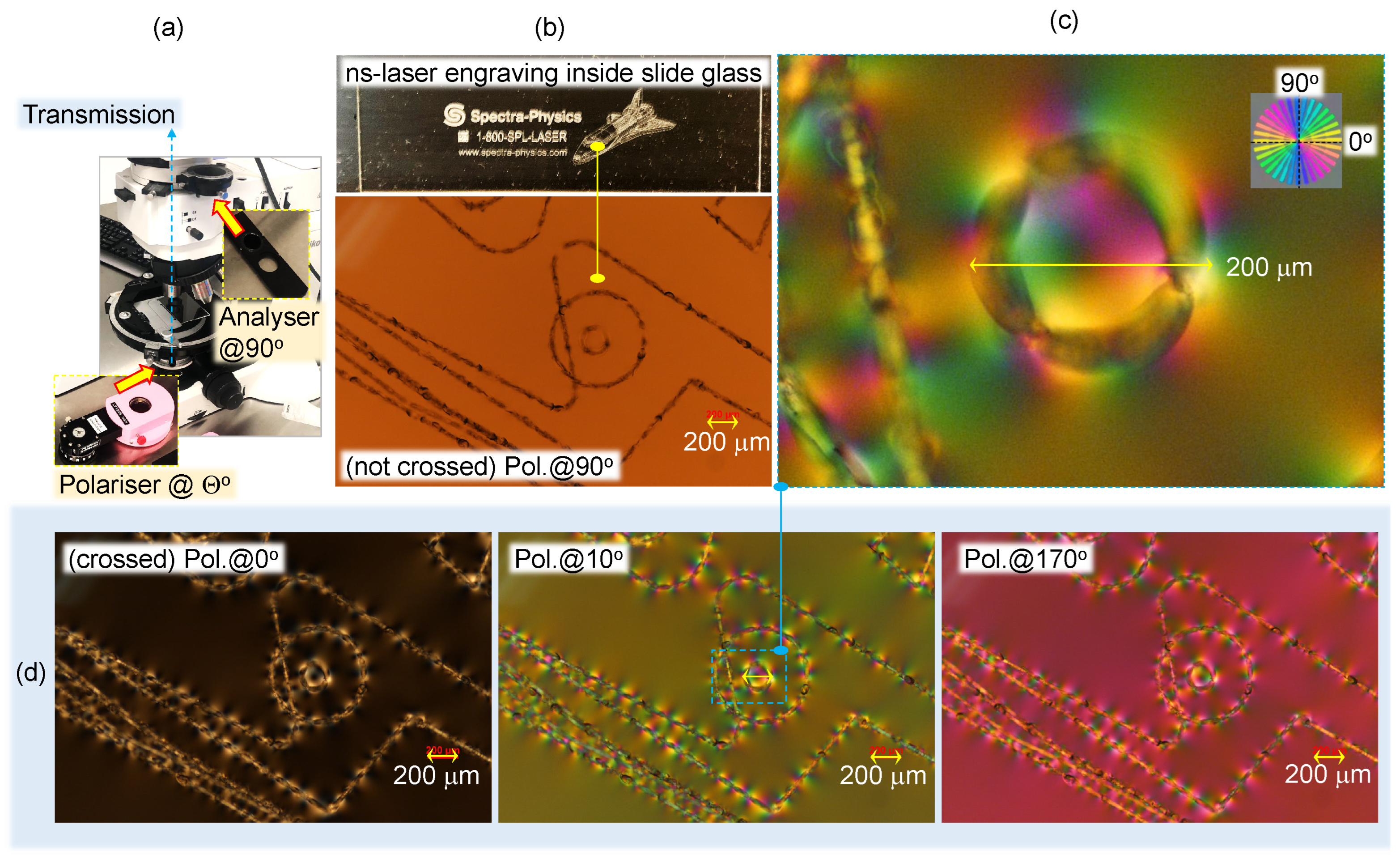
Appendix D. Polarisation Analysis

Visualization of stress inside laser-processed regions inside dielectric materials (glasses and crystals) is usually visualized using a crossed-Nikol setup with an analyzer-polarizer for linear polarization. By using a circularly polarized setup based on optical activity, there is the indifference of orientation for visualization of stress-induced birefringence (Figure A2); in the case of linear polarizers, orientation of stress should be at 45° with respect to the slow/fast axis of the polarizers for highest contrast. Marking traces inscribed with ns-laser pulses have strong stress-induced birefringence around them.
Figure A2. (a) Polychromatic polarization microscope (PPM) based on Nikon Optiphot with circular polarizer-analyzer units for transmission geometry. Polarizers are based on the optical activity (a birefringence for the circularly polarized light). (b) Optical images of a slide-glass with ns-laser-engraved (Hippo, Spectra Physics) pattern [54] (courtesy Dr. M. Li). (c) Closeup view of the ∼200- μ m-diameter circular structure using PPM. (d) PPM images at different settings of the analyzer orientation; θ = 0° corresponds to the cross-Nikol condition.
Photonics 11 00598 g0a2

References

  1. Ng, S.H.; Han, M.; Hyde, L.; Durandet, Y.; Katkus, T.; Zaccaria, R.P.; Juodkazis, S. High Intensity Laser Applications: Space Prospective. In Proceedings of the 2021 Photonics & Electromagnetics Research Symposium (PIERS), Hangzhou, China, 21–25 November 2021; pp. 2670–2677. [Google Scholar]
  2. Mack, C.A. Will stochastics be the ultimate limiter for nanopatterning? In Proceedings of the Novel Patterning Technologies for Semiconductors, San Jose, CA, USA, 25–28 February 2019; Volume 10958, p. 1095803. [Google Scholar]
  3. Malinauskas, M.; Žukauskas, A.; Hasegawa, S.; Hayasaki, Y.; Mizeikis, V.; Buividas, R.; Juodkazis, S. Ultrafast laser processing of materials: From science to industry. Light Sci. Appl. 2016, 5, e16133. [Google Scholar] [CrossRef] [PubMed]
  4. Jain, K.; Dunn, T.J.; Farmiga, N.; Zemel, M.; Weisbecker, C. Large-area high-throughput high-resolution lithography systems for flat-panel displays and microelectronic modules. In Proceedings of the Emerging Lithographic Technologies II, Santa Clara, CA, USA, 23–25 February 1998; Volume 3331, pp. 197–206. [Google Scholar]
  5. McKee, D.C.; Bandera, C. Multistage foveal target detection system. In Proceedings of the Signal Processing, Sensor Fusion, and Target Recognition VII, Orlando, FL, USA, 13–15 April 1998; Volume 3374, pp. 194–203. [Google Scholar]
  6. Jia, W.; Leung, Y.S.; Mao, H.; Xu, H.; Zhou, C.; Chen, Y. Hybrid-Light-Source Stereolithography for Fabricating Macro-Objects With Micro-Textures. J. Manuf. Sci. Eng. 2021, 144, 031003. [Google Scholar] [CrossRef]
  7. Maksimovic, J.; Hu, J.; Ng, S.H.; Katkus, T.; Seniutinas, G.; Rivera, T.P.; Stuiber, M.; Nishijima, Y.; John, S.; Juodkazis, S. Beyond Lambertian light trapping for large-area silicon solar cells: Fabrication methods. Opto-Electron. Adv. 2022, 5, 210086. [Google Scholar] [CrossRef]
  8. Hilfiker, J.N.; Singh, B.; Synowicki, R.A.; Bungay, C.L. Optical characterization in the vacuum ultraviolet with variable angle spectroscopic ellipsometry: 157 nm and below. Proc. SPIE Int. Soc. Opt. Eng. 2000, 3998, 390–398. [Google Scholar]
  9. Kitayama, T.; Itoga, K.; Watanabe, Y.; Uzawa, S. Proposal for a 50 nm proximity x-ray lithography system and extension to 35 nm by resist material selection. J. Vac. Sci. Technol. B Microelectron. Nanometer Struct. Process. Meas. Phenom. 2000, 18, 2950–2954. [Google Scholar] [CrossRef]
  10. Rothschild, M.; Bloomstein, T.M.; Efremow, N.; Fedynyshyn, T.H.; Fritze, M.; Pottebaum, I.; Switkes, M. Nanopatterning with UV Optical Lithography. MRS Bull. 2005, 30, 942–946. [Google Scholar] [CrossRef]
  11. Kozawa, T.; Tagawa, S. Radiation Chemistry in Chemically Amplified Resists. Jpn. J. Appl. Phys. 2010, 49, 030001. [Google Scholar] [CrossRef]
  12. Hua, J.G.; Ren, H.; Huang, J.; Luan, M.L.; Chen, Q.D.; Juodkazis, S.; Sun, H.B. Laser-Induced Cavitation-Assisted True 3D Nano-Sculpturing of Hard Materials. Small 2023, 19, 2207968. [Google Scholar] [CrossRef] [PubMed]
  13. Žemaitis, A.; Gaidys, M.; Brikas, M.; Gečys, P.; Račiukaitis, G.; Gedvilas, M. Advanced laser scanning for highly-efficient ablation and ultrafast surface structuring: Experiment and model. Sci. Rep. 2018, 8, 17376. [Google Scholar] [CrossRef]
  14. Buividas, R.; Mikutis, M.; Juodkazis, S. Surface and bulk structuring of materials by ripples with long and short laser pulses: Recent advances. Prog. Quantum Electron. 2014, 38, 119–156. [Google Scholar] [CrossRef]
  15. Wang, L.; Chen, Q.D.; Cao, X.W.; Buividas, R.; Wang, X.; Juodkazis, S.; Sun, H.B. Plasmonic nano-printing: Large-area nanoscale energy deposition for efficient surface texturing. Light Sci. Appl. 2017, 6, e17112. [Google Scholar] [CrossRef] [PubMed]
  16. Maksimovic, J.; Mu, H.; Han, M.; Smith, D.; Katkus, T.; Anand, V.; Nishijima, Y.; Ng, S.H.; Juodkazis, S. Si-Cr Nano-Alloys Fabricated by Direct Femtosecond Laser Writing. Materials 2023, 16, 1917. [Google Scholar] [CrossRef] [PubMed]
  17. Zhang, Y.; Jiang, Q.; Long, M.; Han, R.; Cao, K.; Zhang, S.; Feng, D.; Jia, T.; Sun, Z.; Qiu, J.; et al. Femtosecond laser-induced periodic structures: Mechanisms, techniques, and applications. Opto-Electron. Sci. 2022, 1, 220005. [Google Scholar] [CrossRef]
  18. Martinez-Calderon, M.; Groussin, B.; Bjelland, V.; Chevallay, E.; Fedosseev, V.N.; Himmerlich, M.; Lorenz, P.; Manjavacas, A.; Marsh, B.A.; Neupert, H.; et al. Hot electron enhanced photoemission from laser fabricated plasmonic photocathodes. Nanophotonics 2024, 13, 1975–1983. [Google Scholar] [CrossRef]
  19. Roques-Carmes, C.; Kooi, S.; Yang, Y.; Massuda, A.; Keathley, P.; Zaidi, A.; Yang, Y.; Joannopoulos, J.; Berggren, K.; Kaminer, I.; et al. Towards integrated tunable all-silicon free-electron light sources. Nat. Commun. 2019, 10, 3176. [Google Scholar] [CrossRef]
  20. Kerse, C.; Kalaycıoğlu, H.; Elahi, P.; Çetin, B.; Kesim, D.K.; Akçaalan, O.; Yavaş, S.; Aşık, M.D.; Öktem, B.; Hoogland, H.; et al. Ablation-cooled material removal with ultrafast bursts of pulses. Nature 2016, 537, 84–88. [Google Scholar] [CrossRef] [PubMed]
  21. Khurgin, J. Energy and Power Requirements for Alteration of the Refractive Index. Light Sci. Appl. 2024, 18, 2300836. [Google Scholar] [CrossRef]
  22. Lin, Z.; Ji, L.; Wang, W. Precision machining of single crystal diamond cutting tool via picosecond laser irradiation. Int. J. Refract. Met. Hard Mater. 2023, 114, 106226. [Google Scholar] [CrossRef]
  23. Marlow, F.; Josten, S.; Leiting, S. Electronics with stainless steel: The work functions. J. Appl. Phys. 2023, 133, 085104. [Google Scholar] [CrossRef]
  24. Neuenschwander, B.; Remund, S.; Nussbaum, C.; Kling, R.; Fritsch, K.; Franke, C.; Ballukonis, D.; Hochner, U. Michromachining of dielectrics and semiconductors with external pulse compression below 100 fs, 2024. In Proceedings of the LPM2024, San Sebastian, Spain, 11–14 June 2024. [Google Scholar]
  25. Gamaly, E.G.; Rode, A.V.; Luther-Davies, B. Ablation of solids by femtosecond lasers: Ablation mechanism and ablation thresholds for metals and dielectrics. Phys. Plasmas 2002, 18, 949–957. [Google Scholar] [CrossRef]
  26. Juodkazis, S.; Okuno, H.; Kujime, N.; Matsuo, S.; Misawa, H. Hole Drilling in Stainless Steel and Silicon by Femtosecond Pulses at Low Pressure. Appl. Phys. A 2004, 79, 1555–1559. [Google Scholar] [CrossRef]
  27. Jonušauskas, L.; Gailevičius, D.; Rekštytė, S.; Baldacchini, T.; Juodkazis, S.; Malinauskas, M. Mesoscale laser 3D printing. Opt. Express 2019, 27, 15205–15221. [Google Scholar] [CrossRef] [PubMed]
  28. Bonse, J.; Baudach, S.; Krüger, J.; Kautek, W.; Lenzner, M. Femtosecond laser ablation of silicon–modification thresholds and morphology. Appl. Phys. A 2002, 74, 19–25. [Google Scholar] [CrossRef]
  29. Gamaly, E.E.; Juodkazis, S.; Nishimura, K.; Misawa, H.; Luther-Davies, B.; Hallo, L.; Nicolai, P.; Tikhonchuk, V. Laser-matter interaction in a bulk of a transparent solid: Confined micro-explosion and void formation. Phys. Rev. B 2006, 73, 214101. [Google Scholar] [CrossRef]
  30. Groussin, B.; Martinez-Calderon, M.; Beldarrain, O.; Rodriguez, A.; Olaizola, S.M.; Marsh, B.A.; Granados, E. Efficient Composite Colorization of Copper by Spatially Controlled Oxidation with Deep-UV Ultrafast Lasers. Adv. Opt. Mater. 2024, 12, 2302071. [Google Scholar] [CrossRef]
  31. Gamaly, E.G.; Madsen, N.R.; Duering, M.; Rode, A.V.; Kolev, V.Z.; Luther-Davies, B. Ablation of metals with picosecond laser pulses: Evidence of long-lived nonequilibrium conditions at the surface. Phys. Rev. B 2005, 71, 174405. [Google Scholar] [CrossRef]
  32. Liu, J.M. Simple technique for measurements of pulsed Gaussian-beam spot sizes. Opt. Lett. 1982, 7, 196–198. [Google Scholar] [CrossRef] [PubMed]
  33. Vanagas, E.; Kudryashov, I.; Tuzhilin, D.; Juodkazis, S.; Matsuo, S.; Misawa, H. Surface nanostructuring of borosilicate glass by femtosecond nJ energy pulses. Appl. Phys. Lett. 2003, 82, 2901–2903. [Google Scholar] [CrossRef]
  34. Vanagas, E.; Kawai, J.; Tuzilin, D.; Kudryashov, I.; Mizuyama, A.; Nakamura, K.G.; Kondo, K.I.; Koshihara, S.Y.; Takesada, M.; Matsuda, K.; et al. Glass cutting by femtosecond pulsed irradiation. J. Microlith. Microfab. Microsyst. 2004, 3, 358–363. [Google Scholar] [CrossRef]
  35. Gaidys, M.; Selskis, A.; Gečys, P.; Gedvilas, M. Stainless steel colouring using burst and biburst mode ultrafast laser irradiation. Opt. Laser Technol. 2024, 174, 110561. [Google Scholar] [CrossRef]
  36. Kretkowski, M.; Jabłoński, R.; Shimodaira, Y. Development of an XYZ Digital Camera with Embedded Color Calibration System for Accurate Color Acquisition. IEICE Trans. Inf. Syst. 2010, E93.D, 651–653. [Google Scholar] [CrossRef]
  37. Kretkowski, M.; Shimodaira, Y.; Jabłoński, R. Color calibration method providing uniform distribution of color difference throughout the whole vision gamut. J. Autom. Mob. Robot. Intell. Syst. 2013, 3, 213–216. [Google Scholar]
  38. Jia, R.; Xiang, S.; Wang, Y.; Chen, H.; Xiao, M. Electrically Triggered Color-Changing Materials: Mechanisms, Performances, and Applications. Adv. Opt. Mater. 2024, 12, 2302222. [Google Scholar] [CrossRef]
  39. Tian, B.; Wang, Z.; Smith, A.T.; Bai, Y.; Li, J.; Zhang, N.; Xue, Z.; Sun, L. Stress-induced color manipulation of mechanoluminescent elastomer for visualized mechanics sensing. Nano Energy 2021, 83, 105860. [Google Scholar] [CrossRef]
  40. Cangueiro, L.; Ramos-de Campos, J.A.; Bruneel, D. Prediction of Thermal Damage upon Ultrafast Laser Ablation of Metals. Molecules 2021, 26, 6327. [Google Scholar] [CrossRef] [PubMed]
  41. Garasz, K.; Kocik, M.; Barbucha, R.; Tański, M.; Petrov, T.; Mohamed-Seghir, M. Optimisation of femtosecond laser micromachining of copper with AI algorithms. J. Achiev. Mater. Manuf. Eng. 2023, 121, 267–274. [Google Scholar]
  42. Greffet, J.J.; Nieto-Vesperinas, M. Field theory for generalized bidirectional reflectivity: Derivation of Helmholtz’s reciprocity principle and Kirchhoff’s law. J. Opt. Soc. Am. A 1998, 15, 2735–2744. [Google Scholar] [CrossRef]
  43. Greffet, J.J.; Carminati, R.; Joulain, K.; Mulet, J.P.; Mainguy, S.; Chen, Y. Coherent emission of light by thermal sources. Nature 2002, 416, 61–64. [Google Scholar] [CrossRef] [PubMed]
  44. Wang, X.; Seniutinas, G.; Balcytis, A.; Kasalynas, I.; Jakstas, V.; Janonis, V.; Venckevicius, R.; Buividas, R.; Appadoo, D.; Valusis, G.; et al. Laser structuring for control of coupling between THz light and phonon modes. arXiv 2016, arXiv:1605.04493. [Google Scholar]
  45. Nishijima, Y.; Balčytis, A.; Naganuma, S.; Seniutinas, G.; Juodkazis, S. Kirchhoff’s metasurfaces towards efficient photo-thermal energy conversion. Sci. Rep. 2019, 9, 8284. [Google Scholar] [CrossRef]
  46. Gibbon, P. Introduction to Plasma Physics. In Proceedings of the CAS-CERN Accelerator School: Plasma Wake Acceleration, Geneva, Switzerland, 23–29 November 2014; Volume CERN-2016-001, pp. 51–65. [Google Scholar]
  47. Gibbon, P.; Förster, E. Short-pulse laser-plasma interactions. Plasma Phys. Control. Fusion 1996, 38, 769–793. [Google Scholar] [CrossRef]
  48. Gibbon, P. Short Pulse Laser Interactions with Matter: An Introduction; World Scientific: Singapore, 2005. [Google Scholar]
  49. Auguste, T.; Monot, P.; Lompre, L.; Mainfray, G.; Manus, C. Multiply charged ions produced in noble gases by a 1 ps laser pulse at λ = 1053 nm. J. Phys. B At. Mol. Opt. Phys. 1992, 25, 4181–4194. [Google Scholar] [CrossRef]
  50. Gibbon, P. Physics of High Intensity Laser Plasma Interactions. In Proceedings of the Varenna Summer School on Laser-Plasma Acceleration, Varenna, Italy, 20–25 June 2011. [Google Scholar]
  51. Normand, D.; Lompre, L.; Comaggia, C. Laser-induced molecular alignment probed by a double-pulse experiment. J. Phys. B At. Mol. Opt. Phys. 1992, 25, L497–L503. [Google Scholar] [CrossRef]
  52. Collett, E. Field Guide to Polarisation; SPIE Press: Bellingham, WA, USA, 2005. [Google Scholar]
  53. Zhou, L.; Li, X.Y.; Zhu, W.J.; Wang, J.X.; Tang, C.J. The effects of pulse duration on ablation pressure driven by laser radiation. J. Appl. Phys. 2015, 117, 125904. [Google Scholar] [CrossRef]
  54. Vanagas, E.; Ye, J.Y.; Li, M.; Miwa, M.; Juodkazis, S.; Misawa, H. Analysis of stress induced by a three-dimensional recording in glass. Appl. Phys. A 2005, 81, 725–727. [Google Scholar] [CrossRef]
Figure 1. (a) Laser CNC machining assembly: laser, stages, and beam scanners for typical fs-laser setup. (b) Laser machining of tooling steel and material cutting section where abrasive micro-sharp materials are bound to the wheel shown at different resolutions (see text for parameter study). The correspondence between the fabrication parameter space can be mapped onto color as a color-to-condition map (see HEX color codes on the two selected matrix patches and their RGB values in (b); made with online tool https://html-color.codes/). These ablation matrices allow parameter dependencies to be explored: power/fluence vs. pulse density, repetition rate vs. scan speed, etc., defining the exposure dose.
Photonics 11 00598 g001
Figure 2. Typical 1 × 1 cm2 Cu coupon samples used to determine ablation rates. Samples were not polished. High and low power ranges were used to explore the different surface roughness and material removal rates of the ablated surfaces (see pulse energy E p and fluence F p [J/cm2]). F-theta lens had focal diameter on the sample 2 r = 60 μ m, depth of focus D o F = 2.7 mm, field of scan 50 × 50 mm2, and axial pulse extent of c t p = 60 μ m for pulse duration of t p = 200 fs. The melting temperature of Cu is 1085 °C, evaporation/boiling point is 2595 °C. For samples Nos. 1 and 2, the focal spot was placed 6 mm deeper along the beam propagation direction from the top surface of the sample. Hatching passes in X-/Y-directions are shown schematically; the total number of passes was always 10.
Photonics 11 00598 g002
Figure 4. SEM images of single-pulse ablation sites (see Figure 3a) at high (a) and low (b) pulse energies on coupons of Cu (a) and Al (b), respectively. The focal spot size is ∼ 60 μ m.
Photonics 11 00598 g004
Figure 5. (a) The 3D image of ablation lines on Cu ( Δ x = 20 μ m; passes = 10). (b) Ablation rate in μ m3/μJ on Cu and Al coupons with 1 and 10 repeated passes at different pulse energies.
Photonics 11 00598 g005
Figure 6. The width vs. pulse fluence w 2 F p [32] for 1030 nm/200 fs/0.1 MHz irradiation of silica glass at scanning speed corresponding to an in-line separation between pulses of Δ x = 20 μ m. The focal spot size is ∼ 60 μ m. Insets show optical transmission and cross-polarized images of the ablated trenches.
Photonics 11 00598 g006
Table 1. Specific volume removal rates γ a [ μ m3/μJ] for λ = 1030 nm, t p = 200 fs pulses.
MaterialPassesPulse Energy ( μ J)Ablation Rate (10−12 m3/J = μ m3/μJ)
Cu10161.67
108002.32
1161.81
18002.43
Al10166.33
108003.57
11610.44
18005.13
Disclaimer/Publisher’s Note: The statements, opinions and data contained in all publications are solely those of the individual author(s) and contributor(s) and not of MDPI and/or the editor(s). MDPI and/or the editor(s) disclaim responsibility for any injury to people or property resulting from any ideas, methods, instructions or products referred to in the content.

