Abstract
The pinhole plate is a key component of the point diffraction interferometer (PDI). The reasonable improvement and simulation of this device would enhance the application of point diffraction interferometry technology during the measurement of wavefronts. The traditional point diffraction interferometry measurement method is easily disturbed by environmental noise, making it difficult to obtain high-precision dynamic measurements. This paper introduces a four-step phase-shift PDI that can be employed in a common optical path. By using the principle of the finite-difference time-domain method (FDTD), a simulation model of the orthogonal polarization point diffraction pinhole plate (OP-PDPP) structure is established. The results show that when Cr is used as the film material in the pinhole plate, the parameters include a film thickness of 150 nm, a pinhole diameter of 2 μm, a wire grid period of 150 nm, and a wire grid width of 100 nm; in addition, the comprehensive extinction ratio of the pinhole plate is the greatest and the diffraction wavefront error is the smallest. Finally, the constructed experimental system is used to test the wavefront of a flat sample with a 25.4 mm aperture, and the test results are compared with those of the ZYGO interferometer. The difference in the peak-to-valley (PV) value between the OP-PDI and the ZYGO interferometer measurement is 0.0028λ, with an RMS value difference of 0.0011λ; this verifies the feasibility of the scheme proposed in this paper. The experimental results show that the proposed OP-PDPP is an effective tool for high-precision dynamic measurement.
1. Introduction
High-precision optical components are widely used in the fields of aerospace, ultraviolet lithography, displacement sensors, and laser nuclear fusion [1,2,3,4,5]. However, the high price of the testing instruments required for high-precision optical components severely limits their use [6,7]. The PDI uses micron-sized pinhole diffraction to generate a nearly ideal spherical wave as a reference wave, which can theoretically achieve nanometer or even sub-nanometer detection accuracy [8]; in addition, it represents a detection method for high-precision optical components. Therefore, it is essential to study the PDI in research.
The point diffraction pinhole plate (PDPP) is the core component of the PDI, and its hole size is in the micron range; this makes processing difficult and costly. Therefore, it is important to simulate and analyze the parameters of the PDPP. In the past 20 years, many researchers have conducted studies that perform simulation analysis of the PDPP. In 2004, Otaki et al. suggested that, due to the pinhole size of the pinhole plate reaching the order of the wavelength, the accurate estimation of the diffracted waves can only be achieved using vector diffraction theory. They conducted a two-dimensional modeling of the pinhole plate and utilized the rigorous coupled wave (RCW) method to obtain the far-field optical field distribution of the diffracted waves [9]. In 2010, Zengxiong Lu et al. from Changchun Institute of Optics, Fine Mechanics and Physics, Chinese Academy of Sciences, carried out a three-dimensional modeling simulation of the pinhole plate in the extreme ultraviolet wavelength band. Then, they analyzed the effects of different pinhole diameters, different numerical aperture sizes, and different polarization states of the incident light on the diffracted wavefront by using the FDTD method for electromagnetic fields. Finally, they explored the asymmetry wavefront error and light intensity uniformity of the diffracted wave [10]. In 2020, Yuankai Chen analyzed the diffracted wavefront quality of a PDPP based on waveguide theory [11].
In the above works, the simulation analysis of PDPP can be divided into two types according to the principle of the analysis method: one type is based on scalar diffraction theory and the other is based on vector diffraction theory. The scalar diffraction theory-based pinhole plate simulation and analysis method is used to determine the optical field distribution of the diffracted wave, considering the pinhole as a transmittance function without thickness. This method greatly simplifies the complexity of determining the diffraction wave light field. However, it cannot analyze situations in which the size of the pinhole is close to or smaller than the wavelength of the incident light. The simulation analysis of PDPP based on vector diffraction theory fully considers the vector characteristics of the optical field, preserves all the light field components, and precisely analyzes the electric field distribution diffracted by the pinhole plate. As such, this paper adopts the PDPP simulation analysis method based on vector diffraction theory. Meanwhile, the designed PDPP is processed, and the PDI based on the PDPP is set up in the laboratory.
The Section 2 of this paper introduces the basic principle of the orthogonal polarization point diffraction interferometer (OP-PDI), which provides a theoretical basis for the design of the pinhole plate; the Section 3 presents the simulation results and analysis, so as to determine the actual parameters of the pinhole plate; the Section 4 describes the optical system of this experiment. Finally, the Section 5 of this study is given.
2. Principle of the OP-PDPP
2.1. Point Diffraction Interference Systems
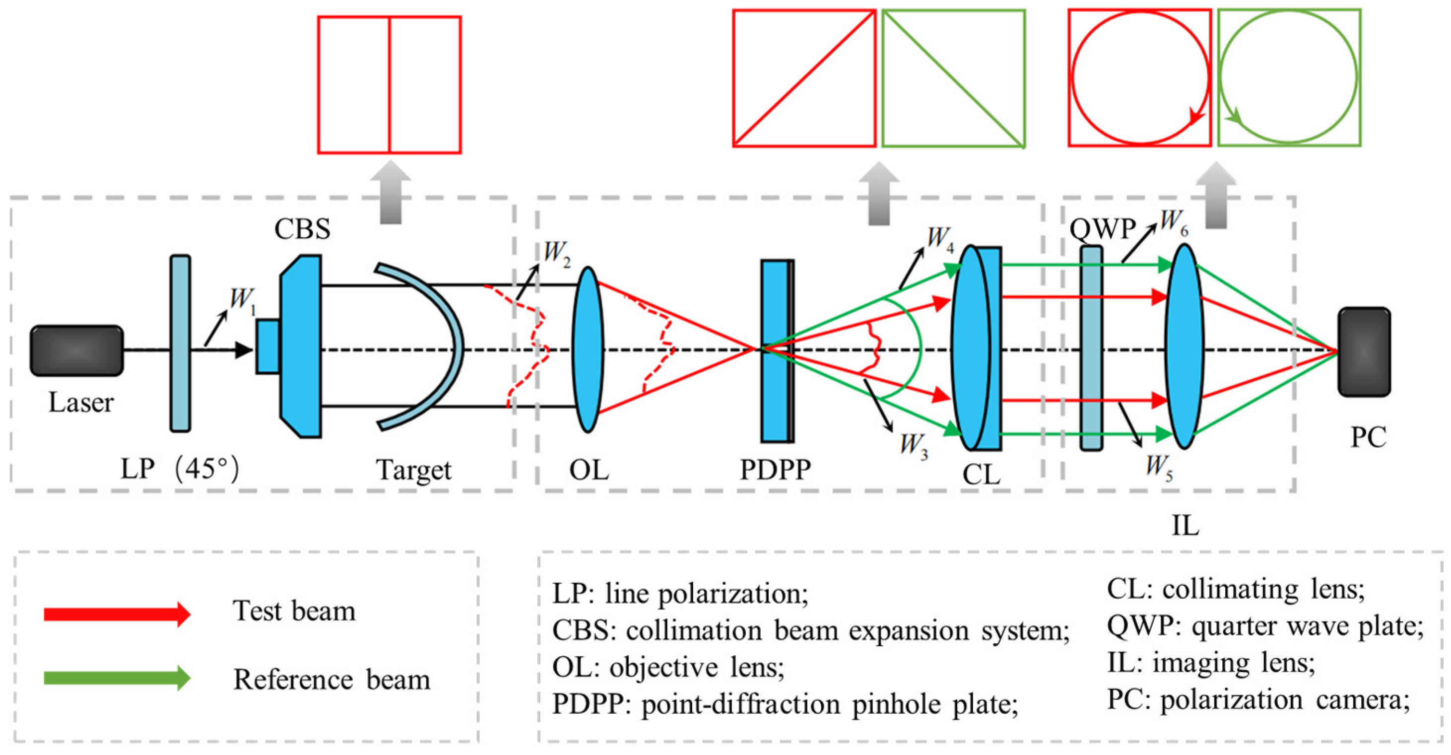
The basic principle of the traditional PDI is as follows: the converging sphere carrying the wavefront information of the target converges at the small hole on the point diffraction plate; then, a portion of the light is diffracted through the pinhole to produce a reference light that approximates a standard spherical wave. The other part of the light directly passes through the point diffraction plate, carrying the wavefront information that is to be measured as the test light. The reference light interferes with the test light so that the interference fringe pattern can be obtained. Then, the wavefront information can be restored from the fringe pattern. Depending on whether the reference light and the test light are on the same optical path, the system can be divided into a common path PDI [12] and a non-common path PDI [13]. The optical path difference of the non-common path PDI is easily affected by environmental vibration and temperature, which leads to the occurrence of unstable interference fringes and affects the detection accuracy of the system. The common optical path PDI can avoid the influence of the optical path difference. However, its reference wavefront is obtained by using a part of the wavefront to be measured for small aperture diffraction. Introducing a phase shift in the optical path is difficult, and this limits the further improvement of its detection accuracy [14]. In this paper, we use an orthogonal polarization common optical path PDI, which can introduce a four-step phase shift in a single shot in order to obtain high-precision dynamic wavefront measurements.
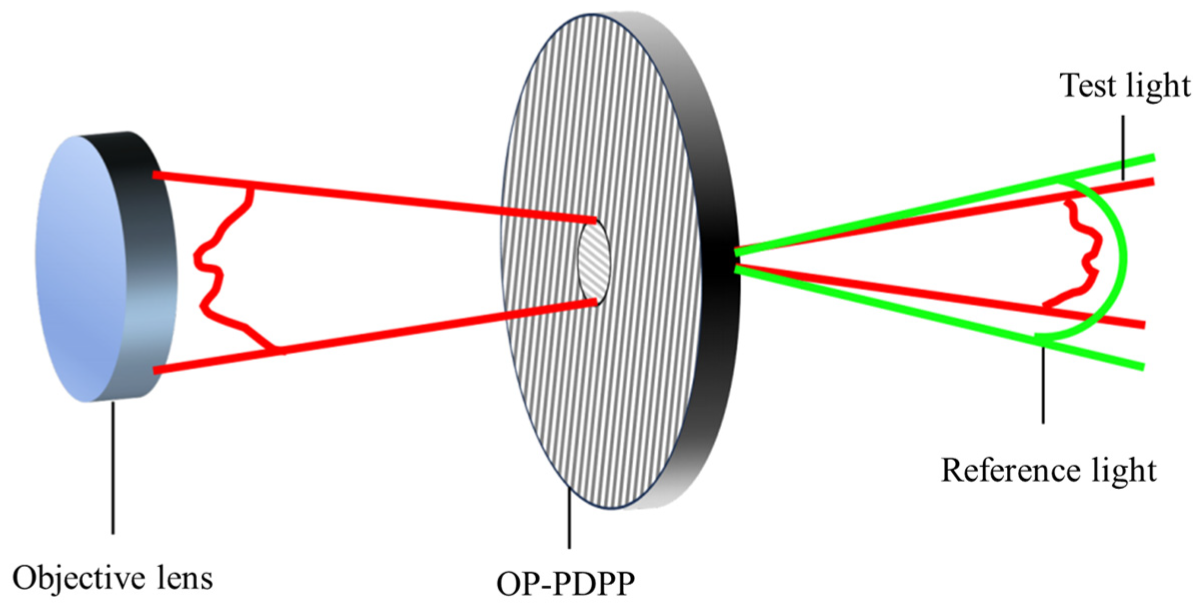
The change in the wavefront of the OP-PDI is shown in Figure 1. The polarization direction and intensity of the linearly polarized light emitted by the He-Ne laser are adjusted by a linear polarizer so that it outputs linearly polarized light (W1). W2 is the linear polarized light that carries information about the surface of the target after it has passed through the beam expander and the component to be tested. Figure 2 shows the specific internal and external structure of the pinhole plate. The pinhole plate that we proposed has mutually orthogonal metal gratings inside and outside the pinhole, which is used to generate four-step phase shifting. W3 is the test light that carries information about the wavefront of the target, in which the polarization direction is perpendicular to the optical axis of the wire grating outside the hole. The reference light (W4) is the light diffracted from the wave (W2) that passes through the inner aperture grating; this generates an ideal spherical wave that is perpendicular to the polarization direction of the grating axis within the aperture, which no longer carries the surface shape information to be measured.
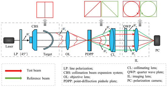
Figure 1.
Wavefront variation diagram of the OP-PDI. The red and green beams represent the test and reference beams, respectively.
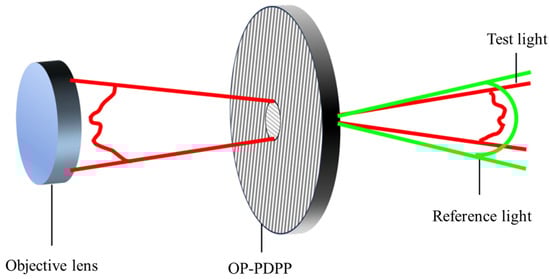
Figure 2.
Schematic diagram of the OP-PDPP.
At this time, the two light waves (W3 and W4) do not interact because their vibration directions are orthogonal to each other. After passing through the quarter-wave plate, the linearly polarized light (W3) carrying the measured surface shape information becomes left-handed circularly polarized light (W5); in addition, the linearly polarized light (W4), which is close to an ideal spherical wave, becomes right-handed circularly polarized light (W6). The two orthogonal circularly polarized lights (W5 and W6), after being focused by an imaging lens, pass through an array-type polarizing camera and are transformed into two beams of linearly polarized light with the same polarization direction; however, these have phase differences of 0, π/2, π, and 3π/2, respectively, after the 0°, 45°, 90°, and 135° linear polarizer. Finally, four interference images with a phase shift of π/2 are presented on the CCD camera.
2.2. Theoretical Model of the OP-PDPP
The OP-PDPP has low requirements regarding the polarization state and the incident angle of the incident light and has good polarization characteristics; these can be used to separate the reference light and the test light using the polarization state in the case of the reference light and the test light in the completely common optical path. The structure of the pinhole plate is shown in Figure 2. The polarization characteristics of the subwavelength metal gratings are used to improve the traditional PDPP. By designing subwavelength metal gratings that are orthogonal to each other inside and outside the small holes, the transmitted light with a polarization state that is perpendicular to the grating can pass through; meanwhile, the reflected light with a polarization state parallel to the grating is absorbed. In this paper, the Jones matrix is used to describe the experimental optical path [15], and the Jones matrix of the light wave that is obtained after transmission through the element to be measured is :
where is the phase information of the target. Equation (1) indicates that the light passing through the element to be measured carries the phase information.
The PDPP with the optical axis of the grating is placed in the hole at an angle of 45° to the horizontal direction, and the Jones matrix of the intra-aperture grating can be expressed as ; is diffracted inside the small hole to obtain the standard spherical reference light.
where is the Jones matrix of the pinhole external grating, and is the test beam that passes outside the hole.
The Jones matrices of the reference light and the test light after passing through the quarter-wave plate are as follows:
The Jones matrices of the reference light and the test light passing through a 0° polarizer are as follows:
From Equations (5) and (6), it can be seen that a 0-phase shift is introduced between the reference light and the test light after the light is passed through the 0° polarizer of the polarization camera. Similarly, by referring to the Jones matrix of the reference light and the test light passing through the 0° polarizer, as mentioned above, it is clear that the reference light and the test light introduce π/2, π, and 3π/2 phase shifts after passing through the 45°, 90°, and 135° polarizers, respectively. We can therefore obtain the entire light propagation process of the four phase-shift interferograms.
3. Simulation Model and Analysis OP-PDPP Based on FDTD
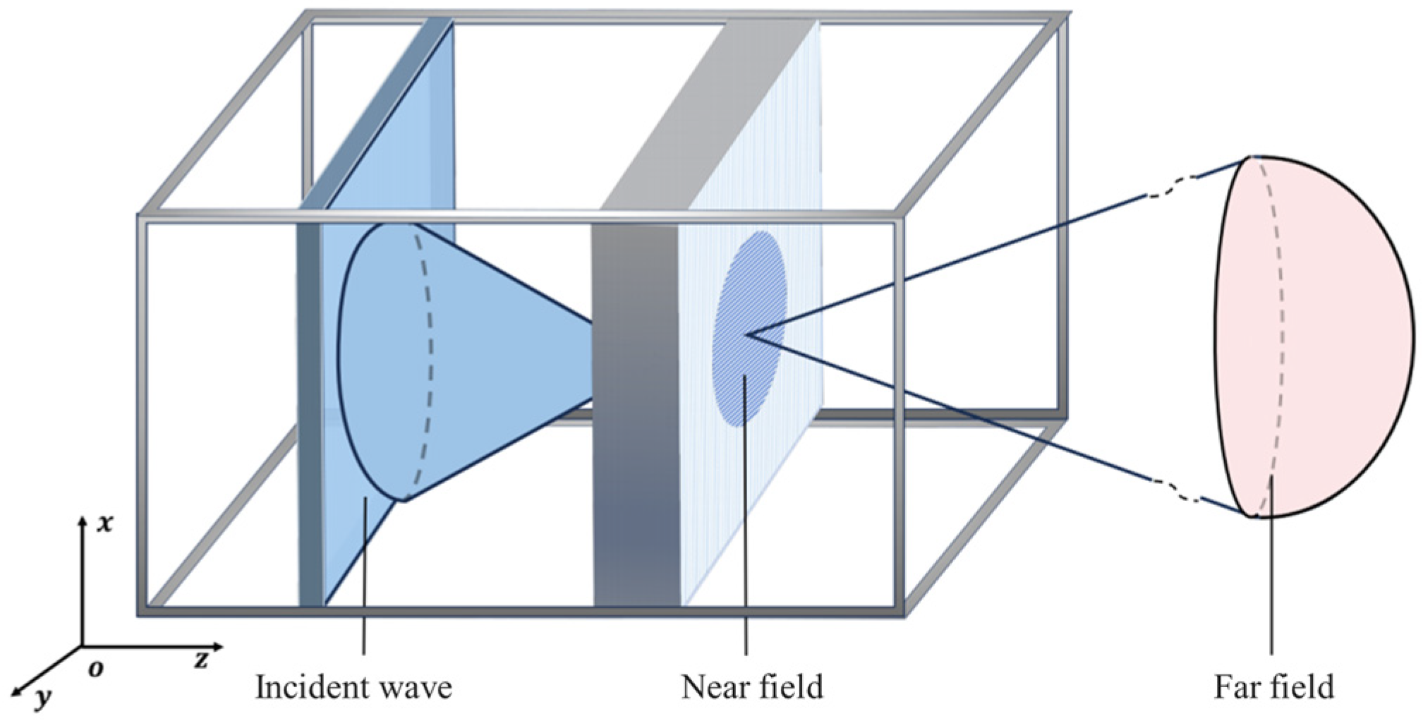
The FDTD method describes the electromagnetic field using the field quantities obtained at a series of discrete points in space and time [16,17]. According to the need for numerical stability, the spatial grid, time step, and cutoff conditions are reasonably selected to ensure that the numerical solution converges to the true solution after the iterative calculations. In the OP-PDI proposed in this paper, the diameter of the pinhole in the pinhole plate is in the sub-micron range, and the scalar diffraction theory cannot strictly describe its diffraction; in order to ensure the accuracy and high precision of the calculation results, the vector diffraction theory is used to model the OP-PDPP. Figure 3 shows the simulation model of the OP-PDPP. The process of constructing the OP-PDPP simulation model mainly involves near-field simulation based on FDTD, near-field long-distance propagation based on vector diffraction theory [18], and an analysis of the quality of the pinhole plate.
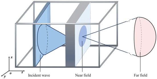
Figure 3.
Simulation model diagram of the OP-PDPP.
Since the beam waist of the converging spot is larger than the size of the small hole in the pinhole plate, the light is considered to exhibit a parallel incidence; therefore, the linearly polarized plane wave with a wavelength of 632 nm is used as the excitation source, and the lengths of the simulation region in the x, y, and z directions are set as x = 1000·Δl = 15.8 μm, y = 1000·Δl = 15.8 μm, and z = 200·Δl = 3.16 μm. In addition, the spatial step size Δl = λ/40 (corresponding to a length of 15.8 nm), and the time step is Δt = Δl/2c. FDTD calculations can only be performed in a limited area, and the calculation space must be artificially truncated, together with the appropriate absorbing boundary conditions. In addition, the perfectly matched layer (PML) [19] with a good absorption effect is selected as the absorbing boundary [20]. According to the field equivalence principle and the Huygens principle, the corresponding far-field distribution is derived from the near-field distribution of the electromagnetic field. The extinction ratio is used to evaluate its polarization performance, and the diffraction wavefront error [21] is used to analyze the quality of the diffraction wavefront.
3.1. OP-PDPP Film Layer Material and Thickness Selection
The PDPP requires metal wire grids with good polarization properties, i.e., a high extinction ratio (ER). The extinction ratio is defined as follows:
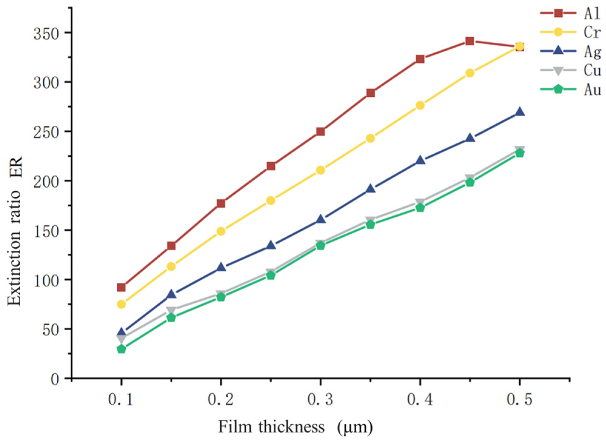
where is the transmittance of the wave, and refers to the transmittance of the wave. In order to determine the material and thickness of the metal wire grating in the OP-PDPP, the FDTD method is used to simulate the polarization characteristics of five common metals when under the same wire grating structure and different thicknesses: these included aluminum (Al), gold (Au), silver (Ag), copper (Cu), and chromium (Cr). The metal wire grid period is 150 nm, the width of the wire grid is 100 nm, the thickness of the wire grid is increased from 100 nm to 500 nm, and the shape of the wire grid is rectangular; the results are shown in Figure 4.
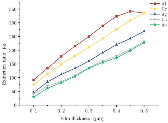
Figure 4.
Influence of the wire grid material and thickness on the extinction ratio.
It can be seen that out of the five metals, namely Cr, Al, Au, Ag, and Cu, Al has the highest extinction ratio, followed by Cr, Cu, Au, and Ag. Due to the active nature of its chemical properties, it is easy to oxidize Al in the air to form a thin film of alumina, and this results in unstable performance. In addition, after a comprehensive consideration of the cost of the metal materials, Cr was selected.
The height of the grating also affects its extinction ratio. When the height of the grating increases from 100 nm to 500 nm, the excessive depth-to-width ratio increases the difficulty of preparing and stripping the grating during lithography, even though the extinction ratio increases with the thickness of the metal grating. To achieve polarization characteristics, the grating’s period needs to be less than the incident wavelength, which is 632 nm. In order to reduce the difficulty associated with processing the grating, a depth-to-width ratio of about 1:3 is more appropriate, so the height of the metal wire grid should be between 100 nm and 200 nm. Because the grating has a significant extinction ratio when the thickness is 150 nm, this paper adopts h = 150 nm as the thickness of the metal grating.
3.2. OP-PDPP Pinhole Size Selection
The pinhole in the pinhole plate is the main structure required to perform point diffraction and generate an ideal spherical reference wavefront. Both the diffraction aperture angle of the reference spherical wavefront produced via diffraction and the wavefront error directly affect the measurement range and accuracy of the OP-PDI; they also have an impact on the quality of the diffracted wavefront and the range of diffraction apertures.
In order to determine the pinhole size of the OP-PDPP, the FDTD method is used to simulate the maximum diffraction aperture angle and the quality of the diffraction wavefront when different pinhole diameters are used. The pinhole plate film is a 150 nm thick chromium film, the line grid period is 100 nm, the width of the line grid is 50 nm, and the diameters of the pinhole are 500 nm, 1000 nm, 1500 nm, 2000 nm, 2500 nm, and 3000 nm, respectively.
- (1)
- The effect of pinhole diameter on the diffraction aperture angle
The maximum diffraction aperture angle is the angle between the beam passing through the edge of the pinhole and the optical axis, which can be expressed as follows:
where dpinhole represents the diameter of the pinhole, λ represents the wavelength of the He-Ne laser, f represents the focal length of the collimating lens, and D represents the diameter of the collimating lens. θmax is the maximum aperture angle.
The maximum aperture angle of the spherical wavefront of pinhole diffraction determines the measurement range of the PDI. The near-field amplitude and phase distributions of the pinhole diffraction obtained using the FDTD method are shown in Figure 5.
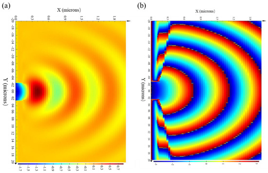
Figure 5.
Near-field distribution, (a) amplitude distribution, and (b) phase distribution of the OP-PDPP.
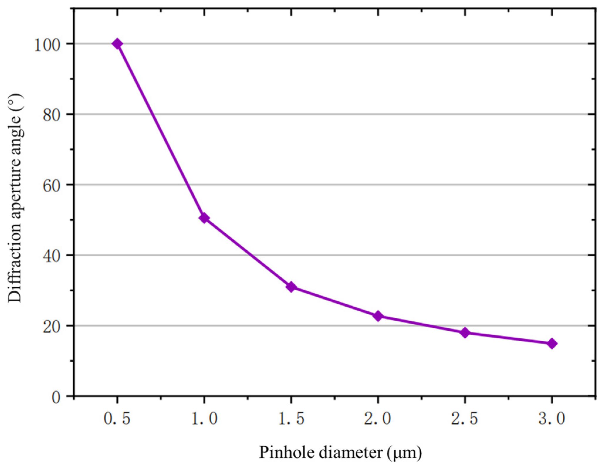
From the figure, it can be seen that the main energy of the diffracted wavefront of the pinhole is concentrated in the range of the diffraction aperture angle. It can also be observed that the distribution of its phase in the range of the diffraction aperture angle is ideal, which is close to the ideal spherical wave. The maximum aperture angle of the diffracted wavefront of the pinhole plates with a diameter of 500 nm, 1000 nm, 1500 nm, 2000 nm, 2500 nm, and 3000 nm is simulated and analyzed, and the results are shown in Figure 6.
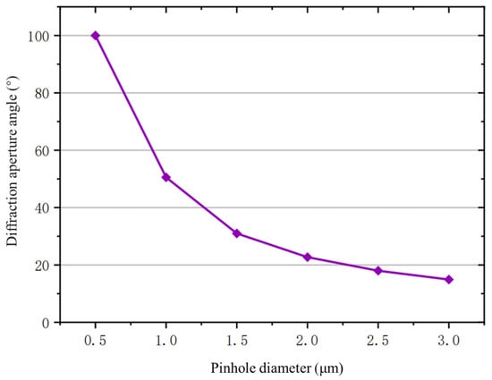
Figure 6.
Influence of the pinhole diameter on the diffraction aperture angle.
The maximum aperture angle of the diffracted wavefront decreases from 100° to 15° as the diameter of the pinhole of the OP-PDPP increases from 500 nm to 3000 nm. The maximum aperture angle before the diffraction wave decreases with the increase in the pinhole diameter of the OP-PDPP.
- (2)
- The effect of pinhole diameter on the quality of diffracted wavefront
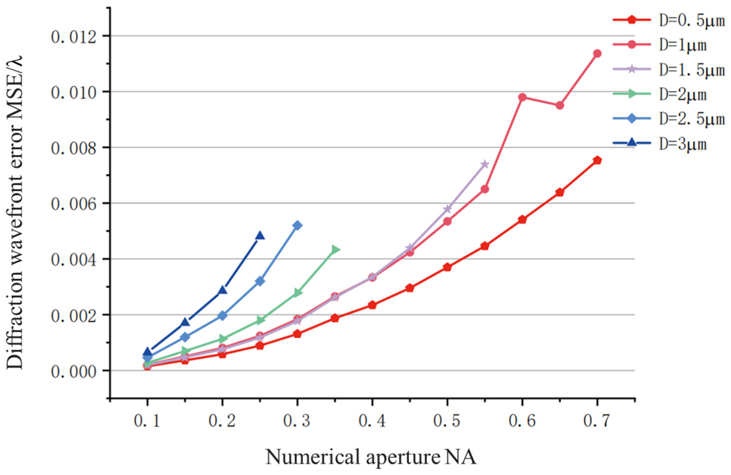
The spherical wavefront error of pinhole diffraction determines the measurement accuracy of the OP-PDI. In order to analyze the diffraction wavefront error corresponding to different pinhole diameters in different numerical aperture ranges, the diffraction wavefront error of pinholes with a diameter of 500 nm, 1000 nm, 1500 nm, 2000 nm, 2500 nm, and 3000 nm is simulated and analyzed, and the results are shown in Figure 7.
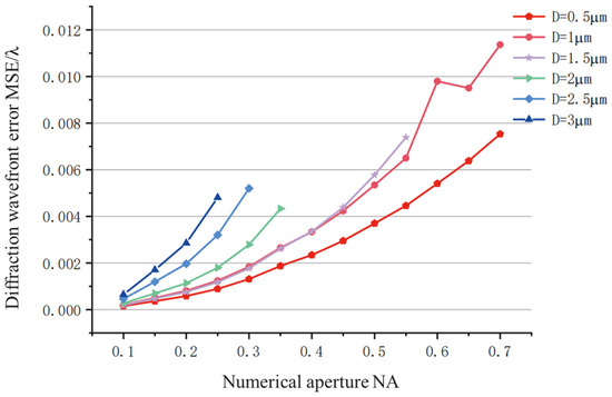
Figure 7.
Diffraction wavefront errors of different pinhole diameters in the range of the corresponding numerical aperture.
When the pinhole plate’s pinhole diameter is certain and the numerical aperture NA is increased from 0.1 to 0.7, the value of the diffraction wavefront error increases with the increase in the numerical aperture NA range. When the numerical aperture range is certain and the pinhole diameter is increased from 0.5 μm to 3 μm, the diffraction wavefront error becomes smaller as the pinhole diameter of the pinhole plate decreases. When the pinhole diameter is 3 μm, the corresponding maximum numerical aperture is 0.25, and the corresponding diffraction wavefront error value is 0.0048λ.
- (3)
- Effect of pinhole diameter on polarization performance
Effect of pinhole diameter on polarization performance
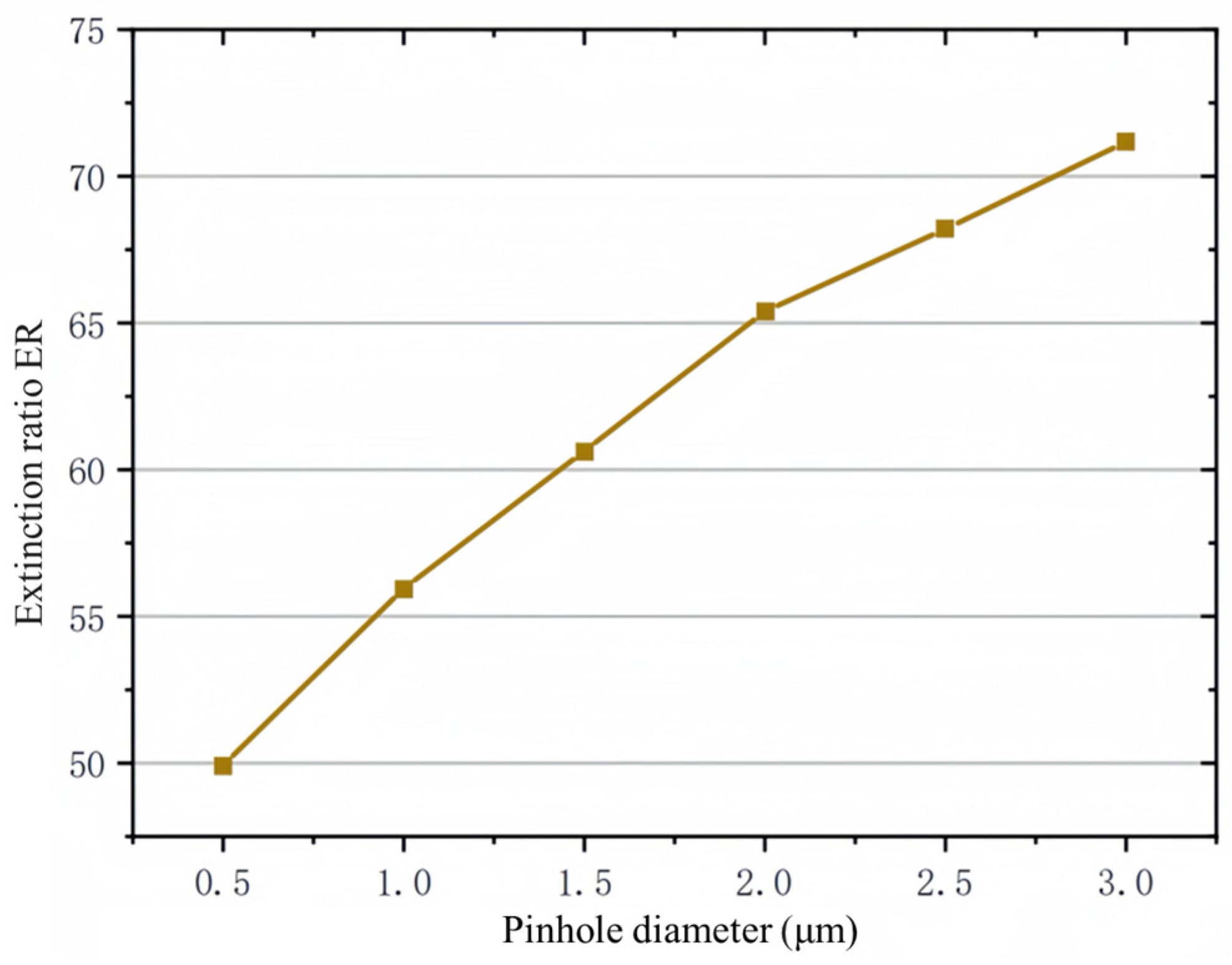
It can be seen from Figure 7 that, with the reduction in the pinhole diameter, the diffraction aperture angle of the pinhole plate increases, and the diffraction wavefront error becomes smaller. However, an excessively small pinhole diameter may affect the polarization performance of the grating in the pinhole region of the OP-PDPP. The polarization performance of the line grid in the pinhole region is simulated and analyzed for pinhole diameters of 500 nm, 1000 nm, 1500 nm, 2000 nm, 2500 nm, and 3000 nm. The results are shown in Figure 8.
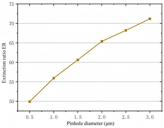
Figure 8.
Extinction ratio of pinhole plate under different pinhole diameters.
As the pinhole diameter increases from 0.5 μm to 3.0 μm, the extinction ratio of the line grating in the pinhole region of the OP-PDPP increases from 50 to 72; in addition, the extinction ratio of the line grating in the pinhole region of the OP-PDPP becomes smaller with the decrease in the pinhole diameter.
In summary, in order to select the pinhole diameter of the OP-PDPP, the effects of the diffraction aperture angle and the polarization performance of the internal grating should be considered simultaneously. According to the above simulation, when the pinhole diameter becomes smaller, the diffraction aperture angle increases, the diffraction wavefront error decreases, and the extinction ratio becomes smaller. Merely reducing the pinhole diameter in the OP-PDPP to improve the quality of the diffraction wavefront and increase the aperture angle can lead to a decrease in the polarization performance of the grating. Therefore, it is necessary to choose the appropriate pinhole diameter to balance these three aspects. When considering the actual range requirements of the point diffraction interferometry numerical aperture and aiming to avoid an excessively small pinhole diameter in the pinhole plate, which may introduce system errors due to increased difficulty associated with alignment, an OP-PDPP with a pinhole diameter of 2 μm should be comprehensively considered.
3.3. OP-PDPP Line Grid Period and Duty Cycle Selection
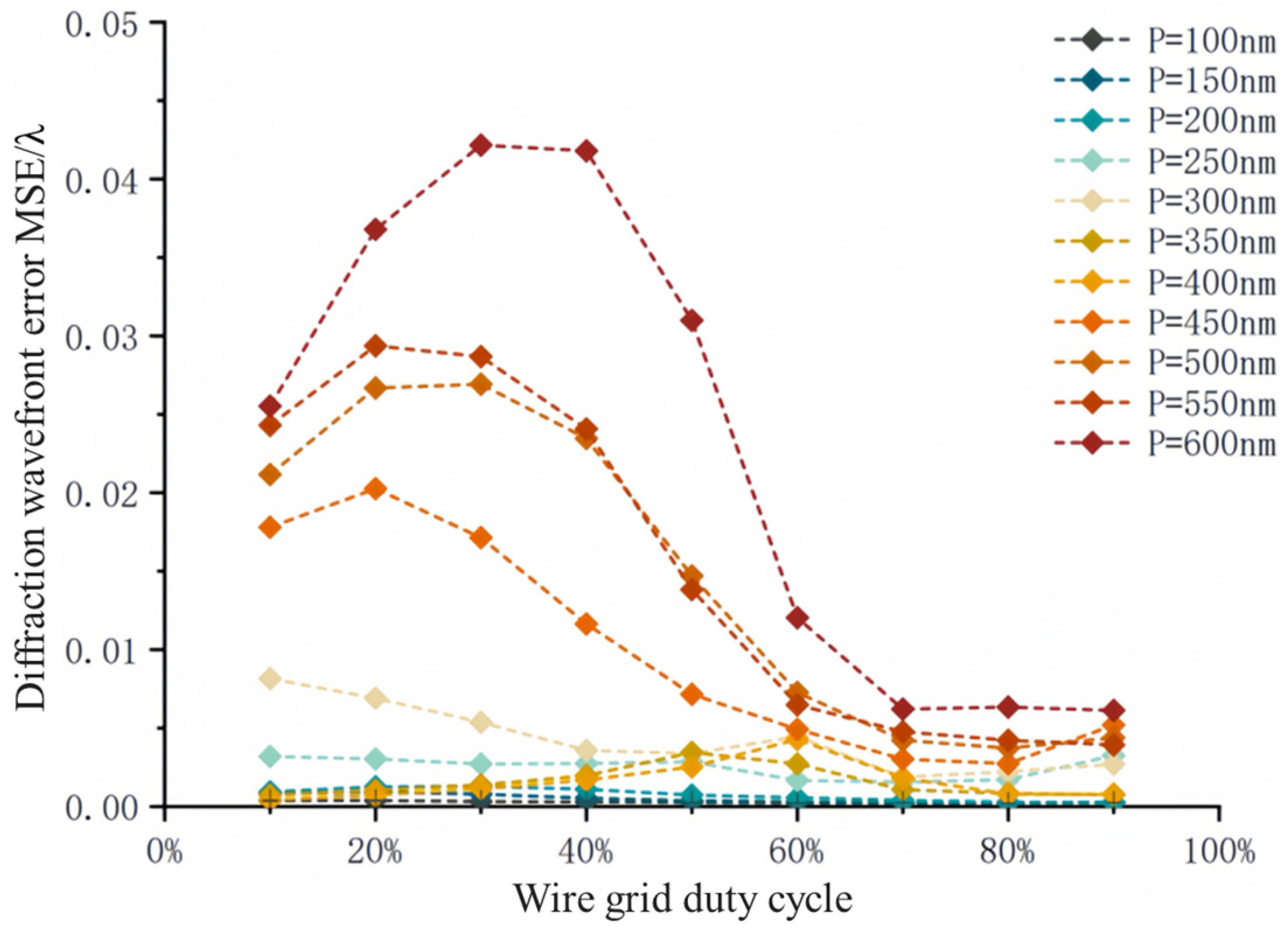
The period and duty cycle of the grid play a decisive role in the polarization properties of the metal wire grid, and these are the most important parameters when designing the structural parameters of the OP-PDPP. To determine the period and duty cycle of the OP-PDPP, the FDTD method is used to simulate the quality of the diffraction wavefront at different grid periods and duty cycle ratios. When the period of the metal wire grid satisfies T < λ/ns, where ns is the refractive index of the substrate, the grid exhibits polarization characteristics. Therefore, the period of the grating should be less than 632 nm. The pinhole plate film is a chromium film with a thickness of 150 nm and a hole diameter of 2 μm. The simulation area for the grid period ranges from 100 nm to 600 nm, with a sampling interval of 50 nm. The simulation area for the grid duty cycle ranges from 10% to 90%, with a sampling interval of 10%. The results are shown in Figure 9.

Figure 9.
Influence of different grid periods and duty ratios on the diffraction wavefront error.
As can be seen in Figure 9, the diffraction wavefront error increases with the increase in the line grid period when the line grid period of the pinhole plate is increased from 100 nm to 600 nm. In addition, the diffraction wavefront error increases and then decreases with the increase in the duty cycle when the line grid duty cycle of the pinhole plate is increased from 10% to 90%.
According to the above simulation, the diffraction wavefront error increases with the increase in the wire grid period. Therefore, it is advisable that the grating period of the pinhole plate is minimized to values within the manufacturing standards. To minimize the diffraction wavefront error, it is advised that the duty cycle of the pinhole plate is maximized to values within the manufacturing standards. Meanwhile, considering the difficulty of the process, the final pinhole plate period chosen is 150 nm, and the width of the grating is 100 nm.
4. Experimental Results and Analysis
- A. Processing of OP-PDPP
The substrate used for the OP-PDPP is sapphire (Al2O3) with dimensions of 25.4 mm × 25.4 mm and a thickness of 500 µm. Magnetron sputtering deposition technology and spin-coating photoresist were used to deposit a thin film of chromium metal on the substrate, and software L-edit was used to draw the required patterns. The instrument then directly wrote the patterns on the sample using electron beam lithography. Inductively coupled plasma (ICP) etching was used to remove the photoresist and form the final pattern on the sample.
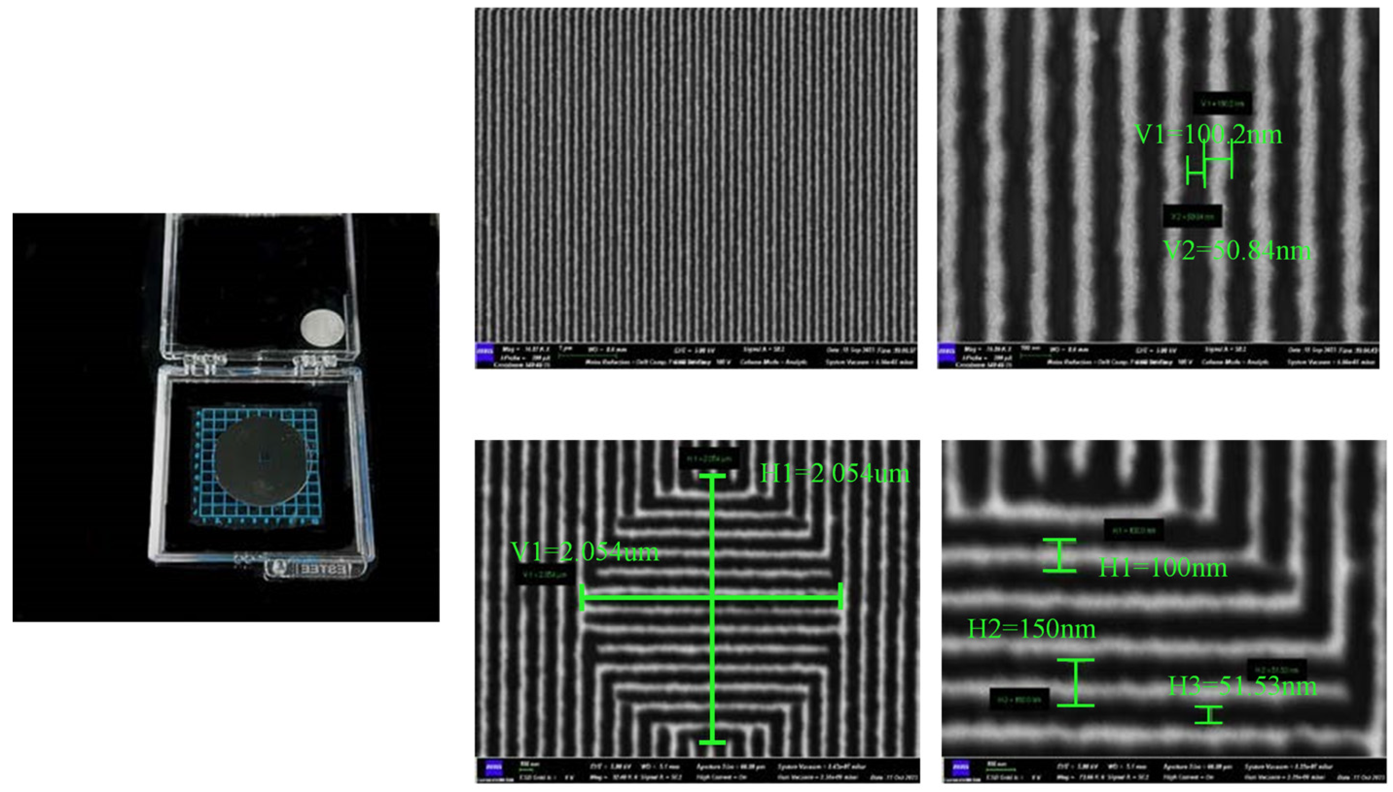
The scanning electron microscopy (SEM) image of the OP-PDPP is shown in Figure 10. The image shows that the diameter of the perforations on the OP-PDPP is approximately 2.004 µm, that the grating period is around 151.04 nm, and that the grating width inside the perforations is 100.2 nm. The processing error is within 5%, and the processing accuracy meets the experimental requirements. This pinhole plate can therefore be used in OP-PDI experimental systems.

Figure 10.
Scanning electron microscopy images of the OP-PDPP.
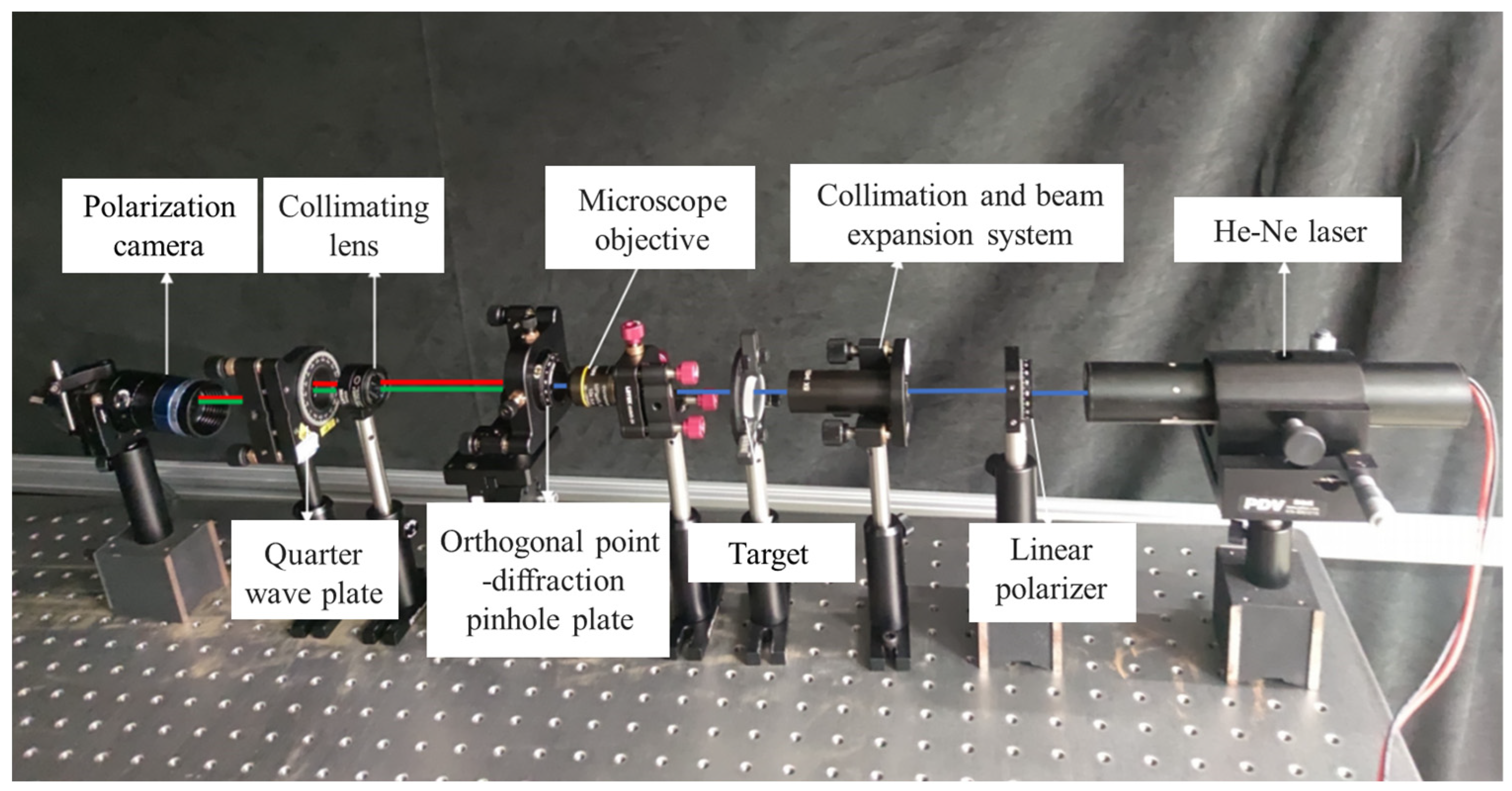
- B. Experiment optical path construction
To validate the feasibility of the OP-PDI proposed in this paper and the accuracy of the measurement results, a detection experiment system based on the fabricated pinhole plate was set up in the laboratory. This system was used to measure the target optical plane, and a linearly polarized He-Ne laser 633-2-P was used as the light source. In addition, the following equipment was employed: a FLP20-VIS thin-film linear polarizer with an operating wavelength in the range of 400 nm–700 nm and an extinction ratio of 5000:1 at 632.8 nm; an LBE633-10 achromatic fixed-magnification laser diffractor; a flat-field semi-refractive achromatic objective of Olympus MPLFLN10X (Tokyo, Japan); a MBCX10609-A laser beam spreader; an MBCX10609-A laser beam spreader; an MBCX10609-A collimating lens; a Molite ML-MC5020XR-18C anti-vibration macro-imaging lens; a Hikvision MV-CH050-10UP (Hangzhou, China) array polarization camera; and a Shanghai Union XYZT60H-10U (Shanghai, China) three-dimensional displacement stage.
To ensure the measurement accuracy of the OP-PDI, the centers of all components in the system should be aligned along the same optical axis. Therefore, the components were aligned precisely by using the pinhole plate with the lowest height as a reference, with the center of the pinhole plate 160 mm away from the optical platform. In the experiment, the polarizing direction of the OP-PDPP was at a 45-degree angle from the horizontal line. When adjusting the polarization direction of the pinhole plate, two linear polarizers and a power meter were needed to adjust the polarization direction in order to maximize the power measured by the power meter. The specific experimental optical setup is shown in Figure 11.
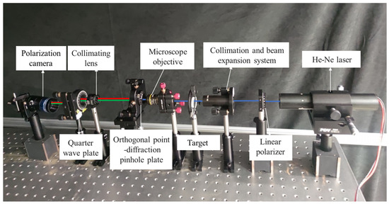
Figure 11.
Optical path of the OP-PDI.
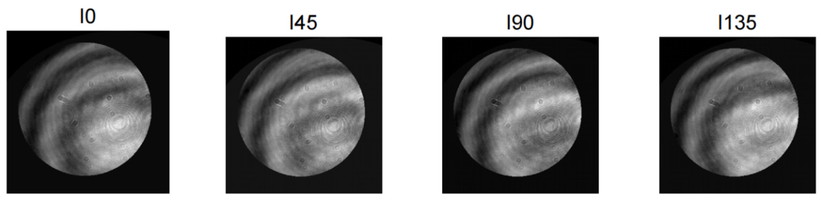
- C. Image Acquisition and Processing
The surface of a quartz flat plate with a diameter of D = 25.4 mm was inspected, and finally, the interferograms were captured on the CCD at four phase shifts. Figure 12 shows the interferograms captured in the experiments.
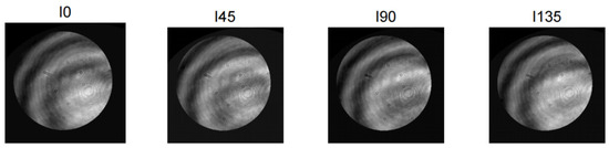
Figure 12.
Interferogram acquired by OP-PDI.
After denoising the interferogram images shown in Figure 12 by using the BM3D denoising algorithm [22], the four-step phase-shifting algorithm was used for phase extraction. I0°, I45°, I90°, and I135° represent the interference intensities captured by the polarized camera under four-step phase shifting. Δϕ represents the phase information of the test surface. The test phase information Δϕ can be obtained by solving the following equation:
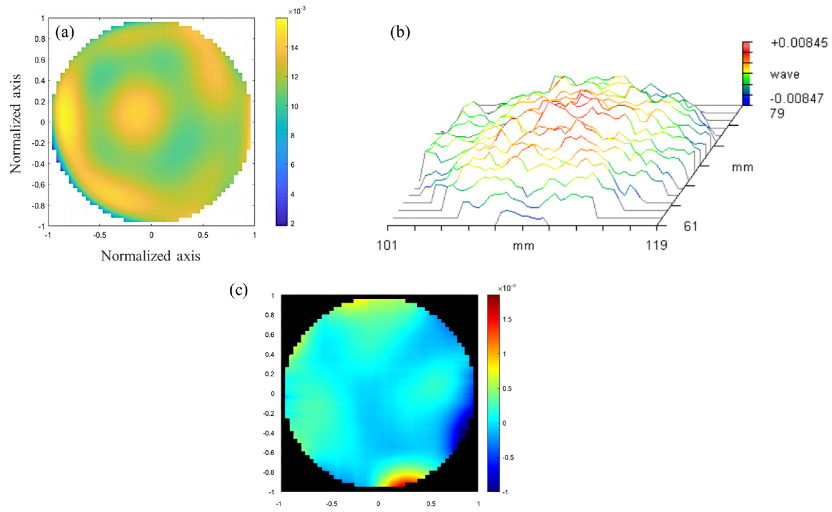
Subsequently, the discrete cosine transform least squares algorithm was used for phase unwrapping [23]; this was followed by the performance of the Zernike polynomial fitting algorithm for wavefront fitting processing. Information regarding the final fitted test surface is shown in Figure 13a, with a peak-to-valley (PV) value of 0.0142λ and a root mean square (RMS) value of 0.0019λ. As shown in Figure 13b, the same test component was examined under the same experimental conditions using the ZYGO interferometer, and the detection results of the ZYGO interferometer showed a PV value of 0.017λ and an RMS of 0.003λ. As shown in Figure 13c, the difference in the PV value between the OP-PDI and the ZYGO interferometer measurement is 0.0028λ, with the RMS value differing by 0.0011λ. The OP-PDI built in this article exhibits an accuracy error of approximately λ/300 compared to standardized commercial interferometers, validating the feasibility of the constructed system and the correctness of the measurement results.
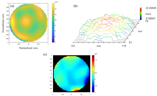
Figure 13.
Results of wavefront distribution. (a) Wavefront distribution of Zernike polynomial fitting result; (b) wavefront distribution of ZYGO; and (c) the difference in the wavefront distribution between the experimental results and the ZYGO.
5. Conclusions
In this paper, we analyze the effects of the pinhole plate film material, film thickness, aperture size, grating period, and grating duty cycle on the extinction ratio and diffraction wavefront quality of a pinhole plate, which is the core element of an OP-PDI; in addition, this analysis is based on the FDTD simulation model. The results show that the best extinction ratio and diffraction wavefront quality are obtained when the OP-PDPP features have a pinhole diameter of 2 μm, a Cr wire grating with a period of 150 nm, a width of 100 nm, and a thickness of 150 nm. In this study, the point diffraction plate is processed and a complete OP-PDI is constructed. The difference in the PV value between the OP-PDI and the ZYGO interferometer measurement is 0.0028λ, with the RMS value differing by 0.0011λ., which proves the feasibility of the OP-PDI.
This work provides a simple and compact structure that avoids the interference of environmental noise and vibration; it can also achieve the high-precision dynamic measurement of the target by introducing four-step phase shifting with an array-type polarized camera in a single shot. The polarization characteristics of the sub-wavelength gratings are then used to solve the problems associated with phase shifting in traditional common-path PDI, providing an effective means of improving the point diffraction pinhole plate.
Author Contributions
Conceptualization, Z.H., W.F., Z.Z. and Q.L.; methodology, Z.H.; investigation, Z.H.; writing, Z.H.; supervision, Q.L. All authors have read and agreed to the published version of the manuscript.
Funding
This paper was supported by the National Natural Science Foundation of China (62004166); the Natural Science Foundation of Zhejiang Province (LY23F040002); and the Natural Science Foundation of Ningbo (202003N4062).
Institutional Review Board Statement
Not applicable.
Informed Consent Statement
Not applicable.
Data Availability Statement
Data are contained within the article.
Conflicts of Interest
The authors declare no conflicts of interest.
References
- Levinson, H.J. High-NA EUV lithography: Current status and outlook for the future. Jpn. J. Appl. Phys. 2022, 61, SD0803. [Google Scholar] [CrossRef]
- van de Kerkhof, M.; Benschop, J.; Banine, V. Lithography for now and the future. Solid State Electron. 2019, 155, 20–26. [Google Scholar] [CrossRef]
- Ma, Z. The Progress and the State-of-Art Facilities of Inertial Confinement Fusion. J. Phys. Conf. Ser. 2022, 2386, 12057. [Google Scholar] [CrossRef]
- Xiao, Q.; Wu, S.; Wang, Y.; Liu, C.; Feng, W.; Yao, Y.; Huang, P.; Wang, X.; Lu, Q. Error analysis and realization of a phase-modulated diffraction grating used as a displacement sensor. Opt. Express 2023, 31, 7907–7921. [Google Scholar] [CrossRef]
- Lu, Q.; Xiao, Q.; Liu, C.; Wang, Y.; Zhu, Q.; Xu, M.; Wang, X.; Wang, X.; Huang, W. Inverse design and realization of an optical cavity-based displacement transducer with arbitrary responses. Opto Electron. Adv. 2023, 6, 220018. [Google Scholar] [CrossRef]
- Li, D.; Wang, R.; Zhang, X. Optical elements based on phase measurement deflection technique. J. Appl. Opt. 2020, 41, 13. [Google Scholar]
- Hou, X.; Zhang, S.; Hu, X.; Quan, H.; Wu, G.; Jia, X.; He, Y.; Chen, Q.; Wu, F. The research progress of surface interferometric measurement with higher accuracy. Opto Electron. Eng. 2020, 47, 200209. [Google Scholar]
- Zhou, Y.; Chang, L.; He, T.; Yu, Y. Detection technology of ultra-precision planar optical elements. Chin. J. Nat. 2023, 45, 157–176. [Google Scholar]
- Lu, Z.; Jin, C.; Zhang, L.; Wang, L. Mass analysis of wavefront by three-dimension pinhole vector diffraction in extreme ultraviolet. Acta Opt. Sin. 2010, 10, 2849–2854. [Google Scholar]
- Lu, Z.; Jin, C.; Ma, D.; Zhang, H. Effect of tiny hole deviation on far-field wavefront quality. Acta Opt. Sin. 2011, 31, 0812002. [Google Scholar]
- Chen, Y.; Bai, J.; Wang, C.; Xue, Y.; Yang, Y. Comparison of Fiber-to-Waveguide Couplers in Point Diffraction Interferometer Based on Waveguide Reference Wavefront Source. Appl. Sci. 2020, 10, 9115. [Google Scholar] [CrossRef]
- Otaki, K.; Bonneau, F.; Ichihara, Y. Absolute measurement of a spherical surface using a point diffraction interferometer. In Proceedings of the Optical Engineering for Sensing and Nanotechnology (ICOSN’99), Yokohama, Japan, 7 May 1999; pp. 602–605. [Google Scholar]
- Gong, Q.; Eichhorn, W. Alignment and testing of piston and aberrations of a segmented mirror. In Proceedings of the Optics and Photonics 2005, San Diego, CA, USA, 19 August 2005; p. 586912. [Google Scholar]
- Zhou, X.; Guo, R.; Zhu, W.; Zheng, D.; Chen, L. Dynamic wavefront measurement with a pinhole linear polarizer point-diffraction interferometer. Appl. Opt. 2017, 56, 8040–8047. [Google Scholar] [CrossRef]
- Yeh, P. Extended Jones matrix method. J. Opt. Soc. Am. 1982, 72, 507–513. [Google Scholar] [CrossRef]
- Dhatt, G.; Lefrançois, E.; Touzot, G. Finite Element Method; John Wiley & Sons: Hoboken, NJ, USA, 2012. [Google Scholar]
- Sullivan, D.M. Electromagnetic Simulation Using The FDTD Method; IEEE Press: Piscataway, NJ, USA, 2013; pp. 1–19. [Google Scholar]
- Lehmkuhl, D. The Equivalence Principle (s). In The Routledge Companion To Philosophy of Physics; Routledge: London, UK, 2021; pp. 125–144. [Google Scholar]
- Ramadan, O. Unsplit-Field PML Algorithm for Truncating Nonlinear FDTD Domains. Int. J. Infrared Millim. Waves 2005, 26, 1151–1161. [Google Scholar] [CrossRef]
- Yu, Z. A simple and effective method for the reflection coefficient extraction in rectangular waveguide discontinuity analysis by the FDTD. Microw. Opt. Technol. Lett. 1997, 15, 57–59. [Google Scholar] [CrossRef]
- Ma, Q.; Liu, W.; Li, X.; Kang, Y.; Wei, Z.; Feng, R.; Liu, H. Analysis of wavefront error of pinhole diffraction in point diffraction interferometer. Acta Opt. Sin. 2008, 28, 2321–2324. [Google Scholar]
- Lu, Q.; Liu, C.; Feng, W.; Xiao, Q.; Wang, X. Deep learning optical image denoising research based on principal component estimation. Appl. Opt. 2022, 61, 4412–4420. [Google Scholar] [CrossRef]
- Zhang, Z.; Wang, X.; Liu, C.; Han, Z.; Xiao, Q.; Zhang, Z.; Feng, W.; Liu, M.; Lu, Q. An efficient and robust phase unwrapping method based on SFNet. Opt. Express 2024, 32, 15410–15432. [Google Scholar] [CrossRef]

Disclaimer/Publisher’s Note: The statements, opinions and data contained in all publications are solely those of the individual author(s) and contributor(s) and not of MDPI and/or the editor(s). MDPI and/or the editor(s) disclaim responsibility for any injury to people or property resulting from any ideas, methods, instructions or products referred to in the content. |
© 2024 by the authors. Licensee MDPI, Basel, Switzerland. This article is an open access article distributed under the terms and conditions of the Creative Commons Attribution (CC BY) license (https://creativecommons.org/licenses/by/4.0/).