Article

Simulation and Analysis of a Near-Perfect Solar Absorber Based on SiO2-Ti Cascade Optical Cavity

1
Joint Laboratory for Extreme Conditions Matter Properties, Key Laboratory of Manufacturing Process Testing Technology of Ministry of Education, State Key Laboratory of Environment-Friendly Energy Materials, Southwest University of Science and Technology, Mianyang 621010, China
2
College of Physics and Electronics, Central South University, Changsha 410083, China
3
School of Physics and Optoelectronic Engineering, Yangtze University, Jingzhou 434023, China
4
School of Chemistry and Chemical Engineering, Jishou University, Jishou 416000, China
5
Department of Physics, Jinzhong University, Jinzhong 030619, China
6
College of Science, Zhejiang University of Technology, Hangzhou 310023, China
7
Guangxi Key Laboratory of Precision Navigation Technology and Application, Guilin University of Electronic Technology, Guilin 541004, China
8
School of Physics and Electronic-information Engineering, Hubei Engineering University, Xiaogan 432000, China
*
Author to whom correspondence should be addressed.
These authors contributed equally to this work.
Photonics 2024, 11(7), 604; https://doi.org/10.3390/photonics11070604
Submission received: 16 May 2024 / Revised: 19 June 2024 / Accepted: 25 June 2024 / Published: 26 June 2024
(This article belongs to the Special Issue Group IV Photonics: Advances and Applications)

Abstract

:
The main development direction for current solar technology is to improve absorption efficiency and stability. To bridge this gap, we design in this paper a structure consisting of two multilayer disc stacks of different radii, one topped by a TiO2 disc and the other by a cascade disc stack composed of SiO2-Ti, for use in thermal emitters and solar absorbers. The innovation of our work is the exploitation of multiple Fabry–Perot resonances in SiO2-Ti cascade optical cavities to develop absorber bandwidths while investigating it in the field of thermal emission and many aspects affecting the efficiency of the absorber. The finite difference time domain method (FDTD) results show absorption averages as high as 96.68% with an absorption bandwidth of 2445 nm (A > 90%) at 280 nm–3000 nm solar incidence and even higher weighted averages as high as 98.48% at 1.5 solar air mass (AM) illumination. In order to investigate the physical mechanisms of our designed absorber in a high absorption state, we analyzed the electric field distributions of its four absorption peaks and concluded that its high absorption is mainly caused by the coupling of multiple Fabry–Perot resonance modes in the cascaded optical cavity. While considering this high efficiency, we also investigated the effect of complex environments such as extreme high temperatures and changes in the angle of incidence of the absorber, and the results show that the thermal radiation efficiency of the emitter is 96.79% at an operating temperature of 1700 K, which is higher than its thermal radiation efficiency of 96.38% at an operating temperature of 1500 K, which is a perfect result. On the other hand, we conclude that the designed structure is independent of polarization, while the absorber still has 88.22% absorption at incidence angles of up to 60°, both in transverse electric (TE) and transverse magnetic (TM) modes. The results of this study can help improve the performance of future solar absorbers and expand their application areas.

1. Introduction

With the large amounts of fossil fuels being consumed, research into diverse energy sources for the future has led to extensive research around the globe, with photovoltaic absorption technology developing extremely fast [1,2,3,4]. Eternal, clean solar energy could be a good substitute for traditional energy sources to solve the growing energy needs of mankind [5,6]. Nowadays, solar energy has been applied in the field of desalination, greenhouse gas reduction, and energy conversion [7,8,9,10] and has a very promising future. However, the efficiency of solar energy conversion has not been deemed satisfactory, and many problems have been faced when investigating it in order to design a perfect absorber. For example, the absorber has a narrow absorption bandwidth [11], the overall absorption efficiency is not high [12], the material structure is not resistant to high temperatures [13], or the absorption angle is too sensitive and not well adapted to actual environmental changes and other shortcomings [14,15].
In order to make up for these shortcomings, people started with the material of absorbers [16] and found that nanoarray-placed precious metals have high optical absorption and excellent electrical conductivity [17,18,19], which is good for solving the problem of the low absorption rate of solar absorbers, but considering limited resources as well as the cost [20,21], it has not been put into practical use in a large number of cases. Many metamaterials have also been studied to achieve perfect performance with the use of artificially orientated synthetic materials, but the achieved performance is limited [22,23,24,25]. Considering the limitations of heavy metals and metamaterials, we choose Ti and its oxide TiO2, which is a potential high-temperature material with a unique energy gap structure that enhances the absorption of photons by the material, which is helpful in extending the bandwidth [26]. And the refractory metal W with a certain thickness can prevent light penetration well so that light will be reflected and scattered inside the absorber, which can then absorb more solar energy well [27]. At the same time, Si and its oxide SiO2 both have good light absorption ability, which makes their performance in the bandwidth of the visible and near-infrared regions tend toward perfection [28]. On the other hand, Surface Plasmon Resonance (SPR) due to shape structure has a significant impact on the absorber’s performance [29,30,31,32,33]. In previous studies, the emergence of equal-width arranged structures of discs of different sizes [34], stacked structures of complex trapezoidal shapes [35], and regularly arranged structures of elliptic and disc arrays [36] showed that highly absorbing physical properties are the result of both SPR and multiple resonance modes [37]. For nanomaterials, this effect is strongly followed by small shape structure changes in the same material [38,39]. Therefore, designing unique shapes to create enhanced local electromagnetic fields on the surface of metallic or semiconducting nanomaterials can help concentrate sunlight near the surface of nanostructures [40,41,42], which improves the light–absorber interaction to increase overall absorption efficiency. And in many studies, SPR technology has been used as a main idea to improve the performance of solar absorbers in a targeted manner.
At the same time, thermal radiation, as a way of transferring energy, is also an indispensable factor in the study of absorbers. Absorbers transfer energy with their surroundings by emitting electromagnetic waves, mainly in the infrared band [43], and when subjected to thermal radiation from the environment, resulting in an increase in temperature on the surface as well as inside the absorber, the elevated temperature is converted into heat energy and lost according to the law of the conservation of energy [44]. At the same time, excessively high temperatures may also damage materials and structures with low melting points, greatly reducing their ability to absorb solar energy.
For this reason, we designed a multilayer stacked nanoarray structure. Firstly, TiO2 discs were introduced in the top layer, and the SPR phenomenon enhanced absorption in the visible wavelength band, followed by the introduction of a cascade disc optical cavity composed of SiO2-Ti. The coupling effect of multiple Fabry–Perot resonances in this optical cavity maintained absorption in the infrared wavelength band, and the coupling effects of the different resonances provided ideas for high-efficiency absorption at long wavelengths for the absorber in the future. The bottom layer was made of Si and W films as the substrate to further improve light absorption and block light transmission, respectively. The simulation shows that the bandwidth with absorption greater than 90% is 2445 nm, the bandwidth with absorption greater than 95% is 2311 nm, and the average absorption in this bandwidth reaches an amazing 98.42%. At 444.5 nm, 980.5 nm, 1796 nm, and 2390.5 nm (visible infrared band), the absorption rates are all approximately 99% with nearly perfect absorption. We also studied the radiation effect at high temperatures of 1500 K and 1700 K. The radiation efficiencies of the two are 96.38% and 96.79%, respectively.

2. Modeling and Structural Parameters of the Absorber

Figure 1a depicts a solar absorber under solar radiation. The structure consists of a periodic array of refractory tungsten and silicon films with a structural period of P = 400 nm, and a silicon film with a thickness of H1 = 50 nm is used to provide excellent light absorption and thermal conductivity. An opaque tungsten metal film with a thickness of D1 = 150 nm was used as a substrate to eliminate light transmission. The uppermost layer is a titanium dioxide disc with a thickness of H3 = 200 nm and a radius of R1 = 80 nm. Titanium dioxide is widely used for solar energy utilization due to its low cost, high temperature resistance, and excellent optical and electrical properties [45]. On the other hand, SiO2, as a common nanomaterial for absorbers, improves absorption by reducing reflected light in the absorber cavity, and for this purpose, a multilayer absorber disc structure with cascaded optical cavities consisting of Ti and SiO2 between the substrate and TiO2 discs was designed. This multilayer disc structure has a radius of R2 = 150 nm, where the SiO2 and Ti films form an optical cavity, which mainly generates multiple Fabry–Perot resonance modes coupled with SPR resonance modes to capture sunlight, thus enhancing the absorption effect. The thickness of the SiO2 film is H2 = 50 nm, and the thickness of the Ti film is D3 = 10 nm. A thick Ti film deposited on the substrate was used as the last optical cavity, with a thickness of D2 = 150 nm [46]. We used planar light with wavelengths from 280 nm to 3000 nm illuminated from above the Z-axis to compute a given model structure while making exactly matched layers in the Z-direction with periodic boundary conditions in the X- and Y-directions. We used a mesh precision of 5 and further divided the thinnest Ti disc structure in the cascade optical cavity with a finer mesh precision of 2. The dielectric constants of Ti, TiO2, Si, SiO2, and W were taken from Palik [47]. The light absorption can be expressed as A = 1 − T − R [48]. Since the transmittance is cancelled out completely, it is shown that T = 0. Therefore, the absorptivity can be expressed as A = 1 − R.

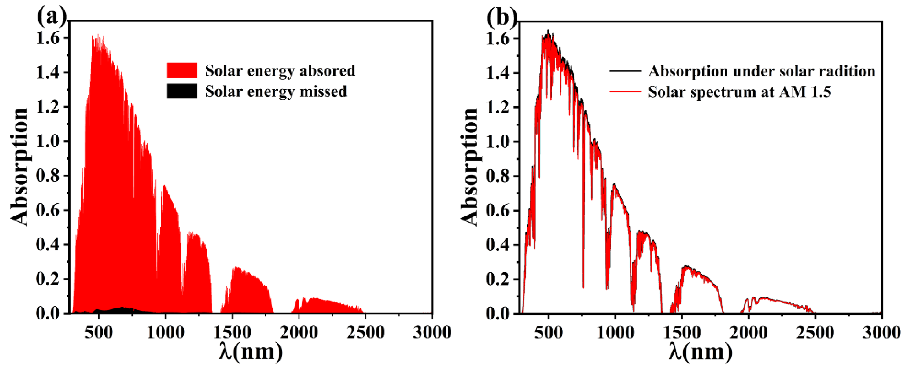
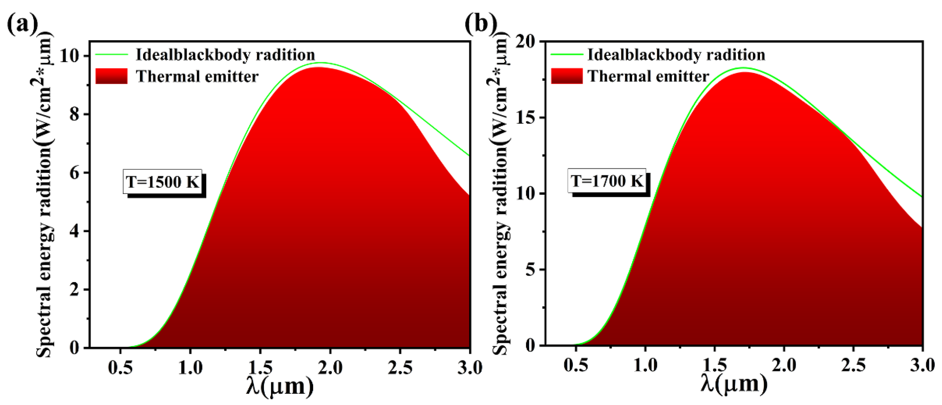
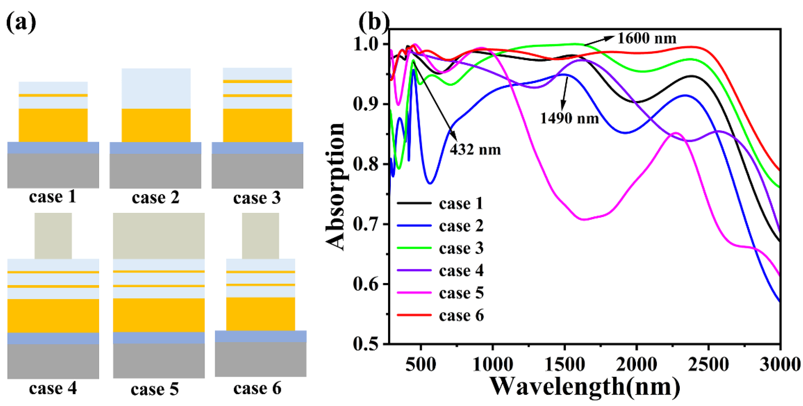
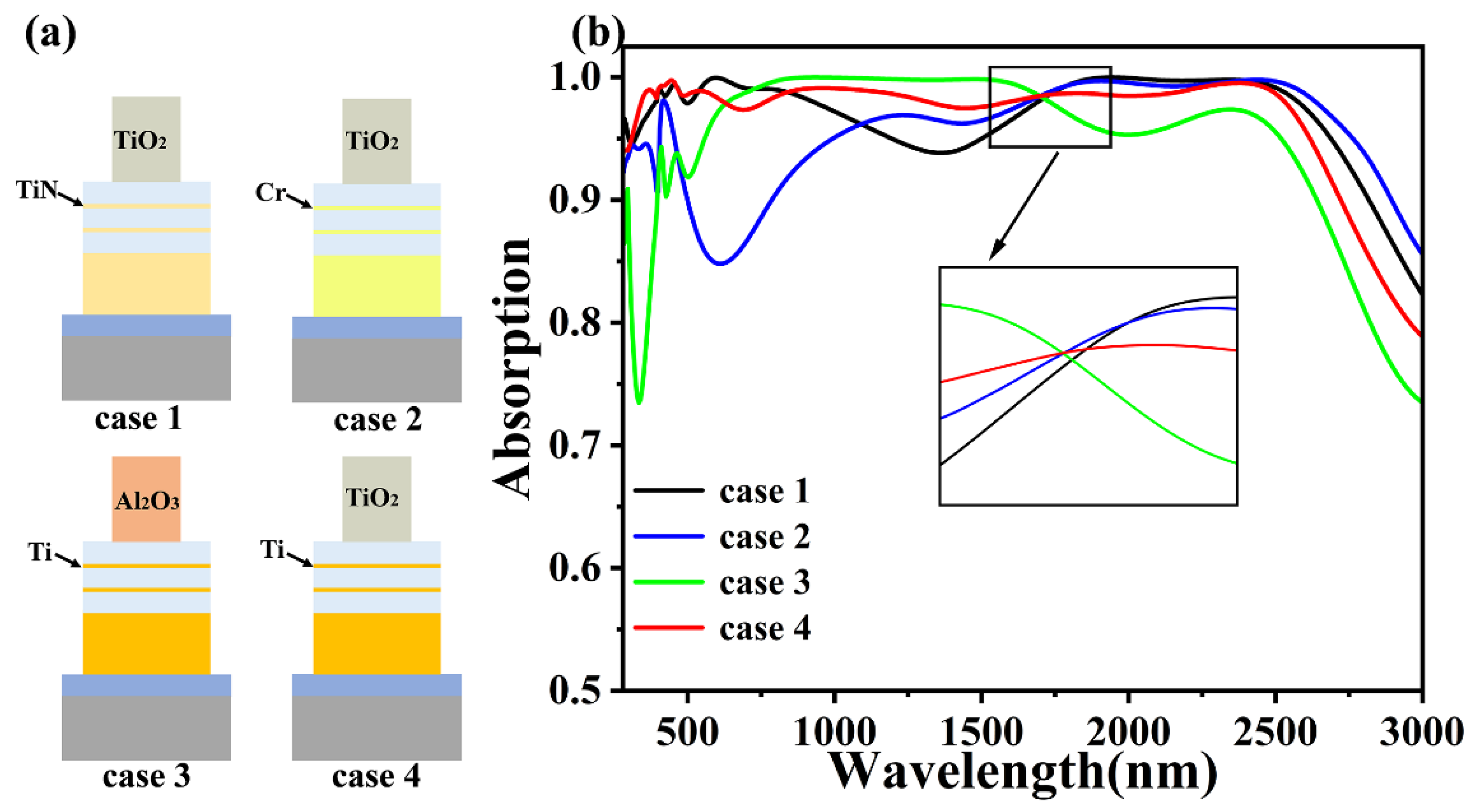
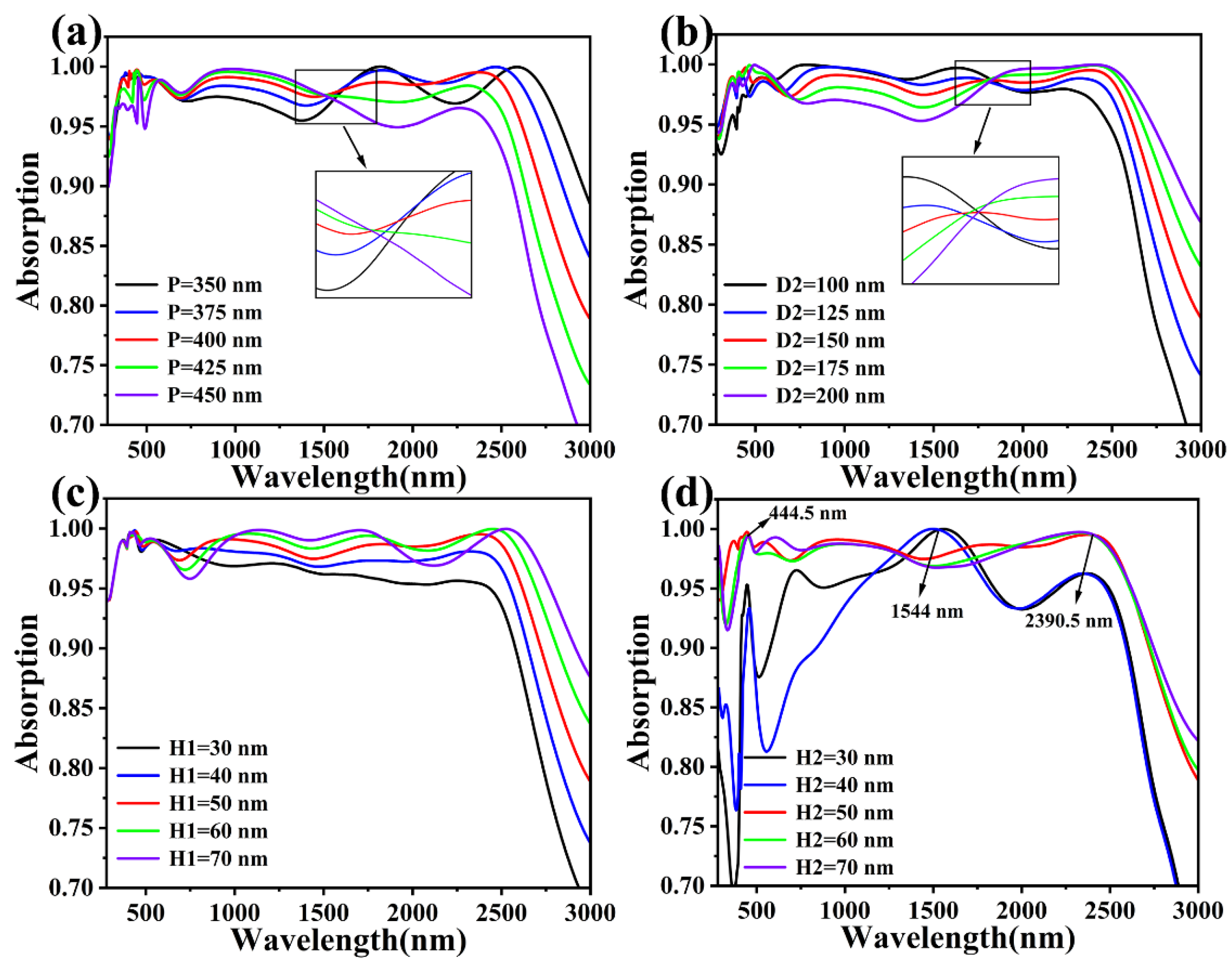
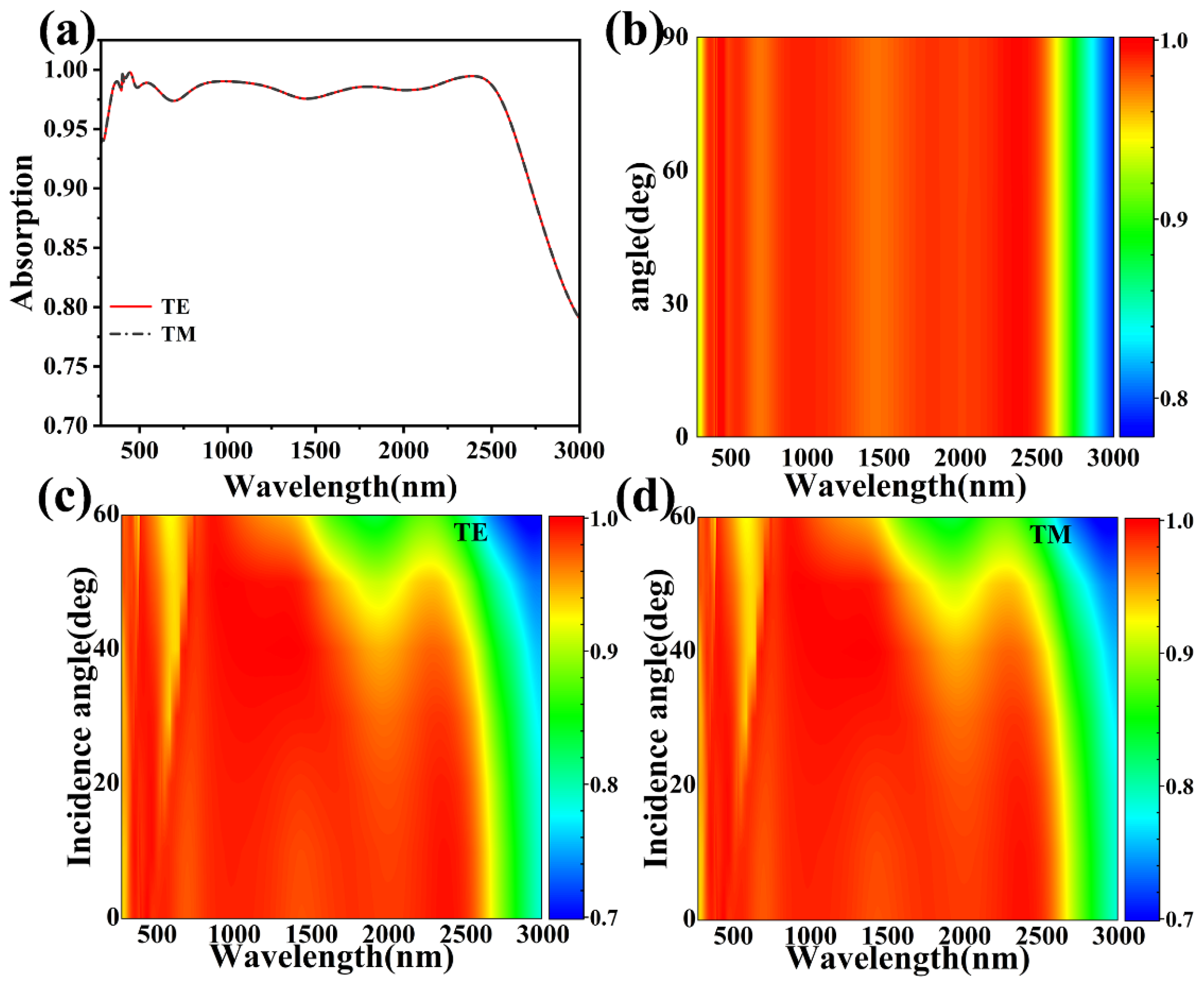
3. Results and Discussion

The absorption is shown in Figure 1b, where it can be seen that the structure exhibits efficient absorption in selected spectra. It can be seen that the average absorption from 280 nm to 2725 nm is as high as 98.12% (A > 90%), with a bandwidth of 2445 nm, which covers the important visible absorption range. It is noteworthy that this also includes the A > 95% band with a bandwidth of 2311 nm, which indicates that the absorber achieves a high-efficiency absorption of A > 95% for most of the available bands. On the other hand, the main absorption losses are in the mid-infrared band after 2390.5 nm. Meanwhile, the innovation of this work is to exploit the multiple Fabry–Perot resonances in the SiO2-Ti cascade optical cavity to increase the absorber’s bandwidth, and in order to discuss later why we can achieve such smooth and highly efficient absorption, we chose four wavelengths with near-perfect absorption intensities, namely λ = 444.5 nm, 980.5 nm, 1796 nm, and 2390.5 nm, respectively. Their absorption intensities reach 99.788%, 99.025%, 98.568%, and 99.463%, respectively, and will be discussed later.
In order to make the simulated near-perfect absorber’s results more reliable, we also investigated its spectral absorptivity when placed under AM1.5. The global spectral equation for AM1.5 incident solar energy is given by Formula (1) [49,50]:
η A = λ M i n λ M a x A ( w ) I A M 1.5 ( w ) d w λ M i n λ M a x I A M 1.5 ( w ) d w
where IAM1.5 (w) is the solar spectral distribution under AM1.5 conditions, and A(w) is the absorptivity of the absorber. Figure 2a shows the energy from the sunlight absorbed and lost by the absorber under AM1.5, with the red region being the absorbed energy and the black region being the lost energy. It can be seen that solar energy is mainly absorbed in the 300–2500 nm band. Meanwhile, the weighted average absorption in the overall band reaches 98.48%, indicating that the absorber loss is very small, which is attributed to a series of effects from multiple light reflections between the designed cascade optical cavity based on the Ti and SiO2 discs.
And in Figure 2b, the red region is the energy spectrum at AM1.5, and the black region is the absorption energy spectrum, which shows that the efficient wavelength range of the solar radiant energy of the absorber is concentrated in the near-UV, visible, and near-infrared bands. The simulation results show that the solar radiation energy spectrum in the AM1.5 band almost coincides with the absorption energy spectrum, and the absorber has a high absorption rate in this band (the average absorption rate, A, from 300 nm to 2500 nm is as high as 98.47%), which confirms that our design for this solar absorber absorbs solar energy very well [51,52].
We also chose 1500 K and the approximate melting point of silicon, which has the lowest melting point among the absorber materials (1700 K), as the simulated ambient temperatures to study the intensity of the thermal emission from the absorber. Figure 3a,b show the thermal emission characteristics of the absorber at elevated temperatures of 1500 K and 1700 K, respectively. In order to evaluate the thermal emission characteristics of the solar absorber, we defined the parameter thermal radiation efficiency (ηE) using Formula (2) [53,54]:
η E = λ M i n λ M a x ε ( w ) · I B E ( w , T ) d w λ M i n λ M a x I B E ( w , T ) d w  
where IBE (w, T) is the ideal blackbody spectral intensity at frequency w and temperature T, and ε(w) is the absorptivity of the surface of the object. As shown in Figure 3a, at a high temperature of 1500 K, we find that only the band around 1500 nm and the infrared band above 2500 nm have a small energy radiation loss, and in all other wavelength ranges, the radiators show a very good fit with the ideal blackbody model, and at this time, the radiation efficiency is 96.38%. As shown in Figure 3b, the losses in the bands around 1500 nm and in the infrared bands above 2500 nm are further compensated at 1700 K, and the thermal radiation efficiency is 96.79%. Since Si has the lowest melting point among the absorber materials we chose, about 1700 K, and any higher temperature would destroy the original absorber structure and material properties, only high temperatures up to 1700 K were investigated, and 1500 K was chosen as a control. It was also concluded that the thermal radiation efficiency of the structure increases with increasing temperature at 1700 K. This is in accordance with the theory in [55], as, at this point, the radiator already exhibits extremely high spectral energy radiation, allowing the radiator to be in the range of 280–2500 nm, showing perfect emission intensity, which further shows that this radiator performs perfectly at high temperatures.
In addition to this, other typical solar absorbers were chosen to compare their results to highlight the superiority of our simulation model. Most of these articles do not analyze the thermal radiation aspect of them, but this does not mean that this aspect is not important. On the contrary, the study of thermal radiators provides a viable way to implement blackbody thermal emission or light sources. The detailed comparison results are shown in Table 1.
SPR in semiconductor nanocrystals as a near-field enhancement phenomenon enables an absorber to obtain light with maximum absorption at the nanoscale level [58,59]. As shown in Figure 4, in order to investigate the stable absorption of the absorber and further physical mechanisms at high radiation intensities, we calculated the electric field of the absorber at the four absorption peak intensities and have included the XOY cross-section and XOZ cross-section of their electric field distributions to illustrate the reasoning.
Figure 4a,e show that at 444.5 nm, the electric field is mainly distributed on the surface of the TiO2 disc and at the junction of the Ti and SiO2 discs, which suggests that the strong absorption at 444.5 nm is induced by the coupling of the SPR of the TiO2 discs and the multiple Fabry–Perot resonance modes at the junction of the Ti and SiO2 discs, which helps maintain the high efficiency of absorption in the visible range. Figure 4b,f show that at 980.5 nm, the influence of the TiO2 disc surface plasma on the absorber diminishes, and the electric field is concentrated in the corner surface region of the cascaded optical cavity multilayer absorber disc array consisting of Ti and SiO2, where the absorption peaks in the corner surface region are determined by the SPR. Figure 4c,d,g,h show that the electric field strength in the corner of the TiO2 disc increases with increasing wavelength, and the plasma resonance effect in the disc part of the cascade optical cavity is also transferred to the lowest Ti disc, but there is no coupling of multiple Fabry–Perot resonance modes at the junction of the Ti and SiO2 discs. On the other hand, with the increase in wavelength after 2390.5 nm in the mid-infrared region, the plasma resonance effect is rapidly transferred from the cascade optical cavity to the bottom of the absorber, so the absorption efficiency of the absorber is strongly affected by the SPR effect in the unique cascade optical cavity designed by us. This leads to a decrease in the absorption in the mid-infrared band after a wavelength of 2390.5 nm. In summary, we can conclude that the smooth broadband absorption and efficient emission of our absorber are dominated by the SPR of the discs and the coupling of multiple Fabry–Perot resonance modes in the cascade optical cavity, where the multiple Fabry–Perot resonance modes in the cascade optical cavity are the main influences on the absorption. Included in this, in the mid-infrared region, the absorption efficiency of the absorber in the wavelength range after 2390.5 nm is mainly affected by the transfer of the plasma resonance to the bottom layer, while a deeper reason is the fact that the absorption efficiency is limited by the compatibility between the SiO2-Ti cascade optical cavities of our design as well as the structure of the absorber. In order to reduce the absorption loss, future solar absorbers can be investigated with semiconductor materials with better Fabry–Perot resonance coupling.
Since the size structure of the model largely determines the SPR of the nanomaterials and thus the absorption properties, there is a pressing need to analyze the different shape structures [60]. Figure 5a shows six cases of different shape structures. Figure 5b shows the absorption of the six different model structures at incident light wavelengths of 280 nm–3000 nm. In these six cases, the structural parameters of the material and the thickness and radius of the film and disc are the same.
As shown in Figure 5b, the difference between case 1 and case 3 is the number of layers in the cascade optical cavity in the middle of our designed absorber, with case 1 having one less recirculation layer than case 3. It can be clearly seen that the overall absorption in the absorption efficiency plot for case 1 is significantly smaller than that for case 3, which is due to the reduced action of the Fabry–Perot resonance coupling therein, suggesting that more than one resonance cavity contributes to the improvement in the overall absorption [61,62]. For cases 2 and 3, the stacking of thinner metal discs of Ti in the SiO2 discs produces a large difference in absorption in the NIR ranges of 1490 nm to 1600 nm, respectively, with better absorption compared to a single conventional dielectric SiO2 disc structure, which reinforces the novelty of our work in introducing SiO2-Ti cascade optical cavities [63,64]. Meanwhile, case 3, compared to the designed structure, lacks a top TiO2 disc, and the absorption is much worse than that in case 6, both in the visible wavelength range at the absorption peak at 432 nm and in the infrared wavelength range after the absorption peak at 1600 nm. So, we explored the effect of the radius of the TiO2 disc and found that the absorption of the TiO2 disc with a large radius fluctuates significantly after continuous optimization. After continuous optimization, we finally determined the optimal coupling radius between the TiO2 disc and the lower cascade optical cavity.
In order to confirm the superiority of the chosen material, we replaced the material in the structure in order to study its absorption properties, as shown in Figure 6. Since the broadband absorption of our designed absorber is a result of the combined effect of the SPR properties of the material and the multiple Fabry–Perot resonances in the cascade optical cavity [65], this also confirms the excellent fit of the absorption between the designed TiO2, SiO2, and Ti discs. In order to investigate whether there is that kind of coupling between combinations of other materials, we verified it with the absorption efficiency. For this purpose, we compared cases 1 and 2 and case 4 by replacing the SiO2-Ti cascade optical cavity discs with SiO2-TiN versus SiO2-Cr structures for observation, respectively. TiN is a better refractory and high-temperature-resistant material than Ti and is commonly used in the fabrication of a wide range of solar absorbers [66]. After the replacement of the SiO2-TiN cascade optical cavity, the absorption in the near-infrared range was unstable, the absorption spectrum showed obvious fluctuations, and the absorption effect in the band never exceeded that of Ti, which is obviously not the result we want. The absorption after replacing the precious metal Cr was even more obviously decreased and unstable, so we did not carry out too much research on this. In case 3, we replaced the top TiO2 disc with another kind of oxide, Al2O3. As can be seen in Figure 6b, case 3 makes up for the disadvantage of the absorption of the TiO2 disc near 1500 nm, but with an increase in NIR wavelengths after 1500 nm, this advantage is rapidly weakened, and the average absorption rate of the disc is 94.54% from 280 nm to 3000 nm, which is far inferior to that of our designed material. For this reason, we chose the SiO2-Ti optical cavity, with stable absorption at 280 nm–3000 nm.
The complex structure of our design makes it difficult to manufacture the absorber, so in daily industrial production, the product will have unavoidable errors. In order to study the effect of these small errors on the absorber, we chose four typical structural parameters in order to explore their effect on the absorber’s absorption. Figure 7a shows a light absorption diagram of the structure with the period increasing from 350 nm to 450 nm and a period interval of 25 nm, and it can be seen that the absorption of the absorber fluctuates over a large range in the whole wavelength band, no matter whether the period, P, is increased from 400 nm to 450 nm or decreased to 350 nm. In the visible band, the absorption at P = 400 nm is more stable than all the other parameters. Figure 7b shows the absorption spectra of the Ti disc in the last resonant cavity in the cascade optical cavity with the height, D2, increased from 100 nm to 200 nm. During the electric field analysis of the absorber, we learned that the strong absorption of visible light is caused by the coupling of the SPR of the TiO2 disc with multiple Fabry–Perot resonance modes at the junction of the Ti and SiO2 discs. So, as D2 increases, it enhances the Fabry–Perot resonance in the cascade optical cavity, which explains why the absorber absorbs better than at D2 = 150 nm in the visible band when D2 increases from 150 nm to 200 nm in Figure 7b. However, after that, in the near-infrared wavelength band, this advantage quickly ceases to exist as the Fabry–Perot resonance decreases for the absorber. Figure 7c,d show the variation in the structural parameters for two thicknesses of the Si film, H1, and the SiO2 disc, H2. In the absorber, the Si film in the substrate does not participate in the near-field coupling; it serves to enhance the multiple absorptions of sunlight in the cascade optical cavity, which largely determines the absorption of light in the absorber. As shown in Figure 7c, with the increase in H1 to 30 nm so that the light is absorbed several times in the cavity, it can be clearly seen that the absorption in the near-infrared wavelength band is gradually enhanced, and the average absorptions in the range of 780 nm–2500 nm are 96.13%, 97.57%, 98.6%, 98.75%, and 98.95% in that order. However, this does not mean the larger the thickness of H1, the better, and this effect is seen in general in the visible wavelength band. After continuous optimization, H1 = 50 nm was finally determined to be the optimal parameter. Figure 7d shows that the absorption of the SiO2 disc with thickness H2 in a multilayer absorbing structural layer increased from 30 nm to 70 nm. As can be seen from the figure, our design of H2 = 50 nm is always in the middle of the five cases for a given range of wavelengths, and an efficient and stable absorption case is desirable.
We chose three wavelengths in the figure, 444.5 nm, 1544 nm, and 2390.5 nm, for our analysis. At a wavelength of 1544 nm, the absorption peaks are seen at H2 = 30 nm and H2 = 40 nm, which are related to the SPR effect at the rounded corners of Ti, but this coupling enhancement drops off very quickly, which also makes the overall absorption efficiency less favorable. The same absorption peaks appear at wavelengths of 444.5 nm and 2390.5 nm for the three cases at H2 = 50, 60, and 70 nm, and the physical mechanism behind them, which we explained during the electric field analysis, cannot be separated from the coupling effect of the SPR with the Fabry–Perot resonance. After that, we conclude that the increase in the thickness of the SiO2 discs increases the distance between the Ti discs in the cascade optical cavity, which leads to a decrease in the near-field coupling of the SPR, and the achieved absorption is ultimately poor, so we determine that H2 = 50 nm is optimal.
For solar absorbers, it is usually necessary to take into account that the actual sunlight is incident from more than one direction, which requires that the absorber we design fulfill the requirement of being angle-insensitive [67]. As shown in Figure 8a,b, we simulate the absorbance maps of the absorber in TE (red) mode and TM (black) mode and give the normalized absorption spectra when the normal polarization angle is varied over a range of 0°–90° (TM polarization to TE polarization). We can find that the absorption curves of the two modes completely overlap, and there is no change in the absorption at each polarization angle as the polarization angle increases from 0° to 90°, which is due to the fact that we designed the structure to be completely symmetric. Figure 8c,d show spectral plots of the change in absorbance in the TE and TM modes with the incidence angle varying from 0° to 60°. In this case, the absorption spectra of both the TE and TM polarization modes are the same, and the average absorptivity of the absorber remains at 88.22% in both polarization modes. Ultra-broadband perfect absorption is achieved at a bandwidth of 2263.5 nm (280 nm–2543.5 nm) (A > 80%) when the angle of incidence is increased up to 60°. It was also found that the permittivity of the waveguide layer decreases as the angle of incidence is increased, which leads to the phenomenon of absorption blueshift [68,69,70,71]. The results show that our designed symmetric broadband absorber can absorb independent of polarization as well as being insensitive to the incident angle.

4. Conclusions

In conclusion, the solar absorber we simulated is a high-efficiency broadband absorber, and the physical mechanism of its high-efficiency absorption mainly lies in the coupling effect between the SPR on the absorber surface and the Fabry–Perot resonance modes under the cascaded disc’s optical cavity, which results in an average absorptivity of 96.68% in the wavelength band 280 nm–3000 nm, with an absorption bandwidth of 2445 nm (A > 90%) and a weighted average solar absorptivity of 98.48% under AM1.5 irradiation. Meanwhile, the thermal radiation efficiency is 96.38% at 1500 K and 96.79% at 1700 K. On the other hand, the material we chose well enhances the absorber’s characteristics of high temperature resistance. At the same time, we found that its high efficiency performance did not drop significantly when we probed for errors in the geometrical parameters of its structure, and its excellent performance far exceeds that of comparable absorbers. Its high efficiency in absorbing incident light at a wide angle in the 280 nm–3000 nm band and its insensitivity to polarization demonstrate its suitability for more complex environments.

Author Contributions

Conceptualization, P.C., Y.Y. (Yingting Yi), Q.S. and Z.Y.; data curation, P.C., Y.Y. (Yingting Yi), Q.S., Z.Y., Y.Y. (Yougen Yi), S.C., J.Z., C.T., T.S. and Q.Z.; formal analysis, P.C. and Z.Y.; methodology, P.C., Y.Y. (Yingting Yi), Q.S., Z.Y., Y.Y. (Yougen Yi), S.C., J.Z. and Q.Z.; resources, P.C., Y.Y. (Yingting Yi), Q.S. and Q.Z.; software, P.C., Y.Y. (Yingting Yi), Q.S., Z.Y., Y.Y. (Yougen Yi), S.C., J.Z. and T.S.; data curation, P.C., S.C. and J.Z.; writing—original draft preparation, P.C.; writing—review and editing, P.C., Y.Y. (Yingting Yi), Q.S., J.Z., C.T., T.S. and Z.Y. All authors have read and agreed to the published version of the manuscript.

Funding

The authors are grateful for the support from the National Natural Science Foundation of China (No. 51606158, 11604311, 12074151); the funding from the Natural Science Foundation of Fujian Province (2022J011102, 2022H0048); the funding from the Guangxi Science and Technology Base and Talent Special Project (No. AD21075009); the funding from the Sichuan Science and Technology Program (No. 2021JDRC0022); the funding from the Natural Science Foundation of Fujian Province (2022J011102); the funding from the Research Project of the Fashu Foundation (MFK23006); the funding from the Open Fund of the Key Laboratory for Metallurgical Equipment and Control Technology of the Ministry of Education in Wuhan University of Science and Technology, China (No. MECOF2022B01; MECOF2023B04); the funding from a project supported by the Guangxi Key Laboratory of Precision Navigation Technology and Application, Guilin University of Electronic Technology (No. DH202321); and the funding from the Scientific Research Project of Huzhou College (2022HXKM07).

Institutional Review Board Statement

Not applicable.

Informed Consent Statement

Not applicable.

Data Availability Statement

Publicly available datasets were analyzed in this study. These data can be found here: [https://www.lumerical.com/]. (accessed on 1 January 2020).

Conflicts of Interest

The authors declare no conflicts of interest.

References

  1. Maksimovic, J.; Hu, J.; Ng, S.H.; Katkus, T.; Seniutinas, G.; Rivera, T.P.; Stuiber, M.; Nishijima, Y.; John, S.; Juodkazis, S.; et al. Beyond Lambertian light trapping for large-area silicon solar cells: Fabrication methods. Opto-Electron. Adv. 2022, 5, 210086. [Google Scholar] [CrossRef]
  2. Xiao, T.; Tu, S.; Liang, S.; Guo, R.; Tian, T.; Müller-Buschbaum, P. Solar cell-based hybrid energy harvesters towards sustainability. Opto-Electron. Sci. 2023, 2, 230011. [Google Scholar] [CrossRef]
  3. Han, Q.C.; Liu, S.W.; Liu, Y.Y.; Jin, J.S.; Li, D.; Cheng, S.B.; Xiong, Y. Flexible counter electrodes with a composite carbon/metal nanowire/polymer structure for use in dye-sensitized solar cells. Solar Energy 2020, 208, 469–479. [Google Scholar] [CrossRef]
  4. Zhang, H.; Feng, L.; Wang, F.; Liu, M.; Zhang, Y.; Zhu, J.; Lu, Y.; Xu, T. Janus aramid nanofiber aerogel incorporating plasmonic nanoparticles for high-efficiency interfacial solar steam generation. Opto-Electron. Adv. 2023, 6, 220061. [Google Scholar] [CrossRef]
  5. Alsaif, H.; Muheki, J.; Ben Ali, N.; Ghachem, K.; Surve, J.; Patel, S.K. Thin-Film Solar Energy Absorber Structure for Window Coatings for Self-Sufficient Futuristic Buildings. Micromachines 2023, 14, 1628. [Google Scholar] [CrossRef]
  6. Hossain, M.J.; Rahman, M.H.; Faruque, M.R.I. An Innovative Polarisation-Insensitive Perfect Metamaterial Absorber with an Octagonal-Shaped Resonator for Energy Harvesting at Visible Spectra. Nanomaterials 2023, 13, 1882. [Google Scholar] [CrossRef]
  7. Zheng, Y.; Zhao, W.C.; Song, Q.J.; Ma, C.; Yi, Z.; Zeng, Q.; Sun, T.; Chen, J.; Yan, J. Analysis of solar absorption and thermal radiation properties of a multi-layer structure. Int. J. Therm. Sci. 2024, 203, 109172. [Google Scholar] [CrossRef]
  8. Atiç, S.; Izgi, E. Smart Reserve Planning Using Machine Learning Methods in Power Systems with Renewable Energy Sources. Sustainability 2024, 16, 5193. [Google Scholar] [CrossRef]
  9. Rugut, E.K.; Maluta, N.E.; Maphanga, R.R.; Mapasha, R.E.; Kirui, J.K. Structural, Mechanical, and Optoelectronic Properties of CH3NH3PbI3 as a Photoactive Layer in Perovskite Solar Cell. Photonics 2024, 11, 372. [Google Scholar] [CrossRef]
  10. Xiong, H.; Deng, J.H.; Yang, Q.; Wang, X.; Zhang, H. A metamaterial energy power detector based on electro-magnetic energy harvesting technology. ACS Appl. Electron. Mater. 2024, 6, 1204–1210. [Google Scholar] [CrossRef]
  11. Lin, K.T.; Lin, H.; Yang, T.; Jia, B. Structured graphene metamaterial selective absorbers for high efficiency and omnidirectional solar thermal energy conversion. Nat. Commun. 2020, 11, 1389. [Google Scholar] [CrossRef]
  12. Gao, M.; Zhu, L.; Peh, C.K.N.; Ho, G.W. Solar absorber material and system designs for photothermal water vaporization towards clean water and energy production. Energy Environ. Sci. 2019, 12, 841–864. [Google Scholar] [CrossRef]
  13. Guan, H.; Hong, J.; Wang, X.; Jingyuan, M.; Zhang, Z.; Liang, A.; Han, X.; Dong, J.; Qiu, W.; Chen, Z.; et al. Broadband, High-Sensitivity Graphene Photodetector Based on Ferroelectric Polarization of Lithium Niobate. Adv. Opt. Mater. 2021, 9, 2100245. [Google Scholar] [CrossRef]
  14. Li, Z.L.; Xie, M.X.; Nie, G.Z.; Wang, J.H.; Huang, L.J. Pushing Optical Virus Detection to a Single Particle through a High Q Quasi-bound State in the Continuum in an All-dielectric Metasurface. J. Phys. Chem. Lett. 2023, 14, 10762–10768. [Google Scholar] [CrossRef]
  15. Cao, T.; Lian, M.; Chen, X.; Mao, L.; Liu, K.; Jia, J.; Su, Y.; Ren, H.; Zhang, S.; Xu, Y.; et al. Multi-cycle reconfigurable THz extraordinary optical transmis-sion using chalcogenide metamaterials. Opto-Electron. Sci. 2022, 1, 210010. [Google Scholar] [CrossRef]
  16. Gigli, C.; Leo, G. All-dielectric χ(2) metasurfaces: Recent progress. Opto-Electron. Adv. 2022, 5, 210093. [Google Scholar] [CrossRef]
  17. Xiong, H.; Ma, X.D.; Wang, B.X.; Zhang, H.Q. Design and analysis of an electromagnetic energy conversion device. Sens. Actuators A Phys. 2024, 366, 114972. [Google Scholar] [CrossRef]
  18. Liang, S.R.; Xu, F.; Li, W.X.; Yang, W.X.; Cheng, S.B.; Yang, H.; Chen, J.; Yi, Z.; Jiang, P.P. Tunable smart mid infrared thermal control emitter based on phase change material VO2 thin film. Appl. Therm. Eng. 2023, 232, 121074. [Google Scholar] [CrossRef]
  19. Zeng, C.; Lu, H.; Mao, D.; Du, Y.; Hua, H.; Zhao, W.; Zhao, J. Graphene-empowered dynamic metasurfaces and metadevices. Opto-Electron. Adv. 2022, 5, 200098. [Google Scholar] [CrossRef]
  20. Yue, Z.; Li, J.T.; Li, J.; Zheng, C.L.; Liu, J.Y.; Lin, L.; Guo, L.; Liu, W. Terahertz metasurface zone plates with arbitrary polarizations to a fixed polarization conversion. Opto-Electron. Sci. 2022, 1, 210014. [Google Scholar] [CrossRef]
  21. Ye, Q.; Chen, M.; Cai, W. Numerically investigating a wide-angle polarization-independent ultra-broadband solar selective absorber for high-efficiency solar thermal energy conversion. Solar Energy 2019, 184, 489–496. [Google Scholar] [CrossRef]
  22. Li, W.; Cheng, S.; Zhang, H.; Yi, Z.; Tang, B.; Ma, C.; Wu, P.; Zeng, Q.; Raza, R. Multi-functional metasurface: Ultra-wideband/multi-band absorption switching by adjusting guided mode resonance and local surface plasmon resonance effects. Commun. Theor. Phys. 2024, 76, 065701. [Google Scholar] [CrossRef]
  23. Fu, R.; Chen, K.X.; Li, Z.L.; Yu, S.H.; Zheng, G.X. Metasurface-based nanoprinting: Principle, design and advances. Opto-Electron. Sci. 2022, 1, 220011. [Google Scholar] [CrossRef]
  24. Luo, J.; Zhang, J.H.; Gao, S.S. Design of Multi-Band Bandstop Filters Based on Mixed Electric and Magnetic Coupling Resonators. Electronics 2024, 13, 1552. [Google Scholar] [CrossRef]
  25. Chen, T.; Pauly, M.; Reis, P.M. A reprogrammable mechanical metamaterial with stable memory. Nature 2021, 589, 386–390. [Google Scholar] [CrossRef]
  26. Wu, L.; Yang, L.L.; Zhu, X.W.; Cai, B.; Cheng, Y.Z. Ultra-broadband and wide-angle plasmonic absorber based on all-dielectric gallium arsenide pyramid nanostructure for full solar radiation spectrum range. Int. J. Therm. Sci. 2024, 201, 109043. [Google Scholar] [CrossRef]
  27. Chang, J.Y.; Taylor, S.; McBurney, R.; Ying, X.; Allu, G.; Chen, Y.B.; Wang, L. Enhancing solar-thermal energy conversion with silicon-cored tungsten nanowire selective metamaterial absorbers. iScience 2021, 24, 101899. [Google Scholar] [CrossRef]
  28. Li, Z.L.; Nie, G.Z.; Wang, J.H.; Zhong, F.; Zhan, S.P. Polarization-modulating switchable and selectable image dis-play through an ultrathin quasi-bound-state-in-the-continuum metasurface. Phys. Rev. Appl. 2024, 21, 034039. [Google Scholar] [CrossRef]
  29. Zhao, H.; Wang, X.K.; Liu, S.T.; Zhang, Y. Highly efficient vectorial field manipulation using a transmitted tri-layer metasurface in the terahertz band. Opto-Electron. Adv. 2023, 6, 220012. [Google Scholar] [CrossRef]
  30. Li, W.X.; Zhao, W.C.; Cheng, S.B.; Zhang, H.F.; Yi, Z.; Sun, T.Y.; Wu, P.H.; Zeng, Q.D.; Raza, R. Tunable Metamaterial Absorption Device based on Fabry–Perot Resonance as Temperature and Refractive Index Sensing. Opt. LaSer Eng. 2024, 181, 108368. [Google Scholar] [CrossRef]
  31. Deng, J.H.; Xiong, H.; Yang, Q.; Wang, B.X.; Zhang, H.Q. Metasurface-based Microwave Power Detector for Polarization Angle Detection. IEEE Sens. J. 2023, 23, 22459–22465. [Google Scholar] [CrossRef]
  32. Fan, J.; Li, Z.; Xue, Z.; Xing, H.; Lu, D.; Xu, G.; Gu, J.; Han, J.; Cong, L. Hybrid bound states in the continuum in terahertz metasurfaces. Opto-Electron. Sci. 2023, 2, 230006. [Google Scholar] [CrossRef]
  33. Liang, X.; Guan, H.; Luo, K.; He, Z.; Liang, A.; Zhang, W.; Lin, Q.; Yang, Z.; Zhang, H.; Xu, C.; et al. Van der Waals integrated LiNbO3/WS2 for High-Performance UV-Vis-NIR Photodetection. Laser Photonics Rev. 2023, 17, 2300286. [Google Scholar] [CrossRef]
  34. Liu, Z.; Liu, G.; Liu, X.; Wang, Y.; Fu, G. Titanium resonators based ultra-broadband perfect light absorber. Opt. Mater. 2018, 83, 118–123. [Google Scholar] [CrossRef]
  35. Chen, M.; He, Y.; Ye, Q.; Zhu, J. Tuning Plasmonic Near-Perfect Absorber for Selective Absorption Applications. Plasmonics 2019, 14, 1357–1364. [Google Scholar] [CrossRef]
  36. Li, J.K.; Chen, X.F.; Yi, Z.; Yang, H.; Tang, Y.J.; Yi, Y.; Yao, W.T.; Wang, J.Q.; Yi, Y.G. Broadband solar energy absorber based on monolayer molybdenum disulfide using tungsten elliptical arrays. Mater. Today Energy 2020, 16, 100390. [Google Scholar] [CrossRef]
  37. Bao, Z.; Wang, J.; Hu, Z.D.; Chen, Y.; Zhang, C.; Zhang, F. Coordination multi-band absorbers with patterned irrelevant graphene patches based on multi-layer film structures. J. Phys. D Appl. Phys. 2021, 54, 505306. [Google Scholar] [CrossRef]
  38. Huang, Y.; Xiao, T.; Chen, S.; Xie, Z.; Zheng, J.; Zhu, J.; Su, Y.; Chen, W.; Liu, K.; Tang, M.; et al. All-optical controlled-NOT logic gate achieving direction-al asymmetric transmission based on metasurface doublet. Opto-Electron. Adv. 2023, 6, 220073. [Google Scholar] [CrossRef]
  39. Li, W.X.; Liu, Y.H.; Ling, L.; Sheng, Z.X.; Cheng, S.B.; Yi, Z.; Wu, P.H.; Zeng, Q.D.; Tang, B.; Ahmad, S. The tunable absorber films of grating structure of AlCuFe quasicrystal with high Q and refractive index sensitivity. Surf. Interfaces 2024, 48, 104248. [Google Scholar] [CrossRef]
  40. Huang, Z.; Zheng, Y.; Li, J.; Cheng, Y.; Wang, J.; Zhou, Z.K.; Chen, L. High-Resolution Metalens Imaging Polarimetry. Nano Lett. 2023, 23, 10991–10997. [Google Scholar] [CrossRef]
  41. Gao, H.; Fan, X.; Wang, Y.; Liu, Y.; Wang, X.; Xu, K.; Deng, L.; Zeng, C.; Li, T.; Xia, J.; et al. Multi-foci metalens for spectra and polarization ellipticity recognition and reconstruction. Opto-Electron. Sci. 2023, 2, 220026. [Google Scholar] [CrossRef]
  42. Wang, B.X.; Duan, G.Y.; Lv, W.Z.; Tao, Y.; Xiong, H.; Zhang, D.Q.; Yang, G.F.; Shu, F.Z. Design and experimental realization of triple-band electromagnetically induced transparency terahertz metamaterials employing two big-bright modes for sensing applications. Nanoscale 2023, 15, 18435–18446. [Google Scholar] [CrossRef]
  43. Liang, S.; Cheng, S.; Zhang, H.; Yang, W.; Yi, Z.; Zeng, Q.; Tang, B.; Wu, P.; Ahmad, S.; Sun, T. Structural color tunable intelligent mid-infrared thermal control emitter. Ceram. Int. 2024, 50, 23611–23620. [Google Scholar] [CrossRef]
  44. Zhang, Y.; Yi, Y.; Li, W.; Liang, S.; Ma, J.; Cheng, S.; Yang, W.; Yi, Y. High Absorptivity and Ultra-Wideband So-lar Absorber Based on Ti-Al2O3 Cross Elliptical Disk Arrays. Coatings 2023, 13, 531. [Google Scholar] [CrossRef]
  45. Li, W.; Elzatahry, A.; Aldhayan, D.; Zhao, D. Core–shell structured titanium dioxide nanomaterials for solar energy utilization. Chem. Soc. Rev. 2018, 47, 8203–8237. [Google Scholar] [CrossRef] [PubMed]
  46. Chen, J.; Guo, J.; Chen, L. Super-wideband perfect solar light absorbers using titanium and silicon dioxide thin-film cascade optical nanocavities. Opt. Mater. Express 2016, 6, 3804–3813. [Google Scholar] [CrossRef]
  47. Palik, E.D. Handbook of Optical Constants of Solids I–III; Academic Press: Orlando, FL, USA, 1998. [Google Scholar]
  48. Li, W.; Yi, Y.; Yang, H.; Cheng, S.; Yang, W.X.; Zhang, H.; Yi, Z.; Yi, Y.; Li, H. Active Tunable Terahertz Band-width Absorber Based on single layer Graphene. Commun. Theor. Phys. 2023, 75, 045503. [Google Scholar] [CrossRef]
  49. Zhang, Y.; Pu, M.; Jin, J.; Lu, X.; Guo, Y.; Cai, J.; Zhang, F.; Ha, Y.; He, Q.; Xu, M.; et al. Crosstalk-free achromatic full Stokes imaging polarimetry metasurface enabled by polarization-dependent phase optimization. Opto-Electron. Adv. 2022, 5, 220058. [Google Scholar] [CrossRef]
  50. Luo, J. Dynamical behavior analysis and soliton solutions of the generalized Whitham–Broer–Kaup–Boussineq–Kupershmidt equations. Results Phys. 2024, 60, 107667. [Google Scholar] [CrossRef]
  51. Zheng, Y.; Wang, Z.Y.; Yi, Z.; Cheng, S.B.; Ma, C.; Tang, B.; Sun, T.Y.; Yu, S.J.; Li, G.F.; Ahmad, S. A wide-band solar absorber based on tungsten nano-strip resonator group and graphene for near-ultraviolet to near-infrared region. Diam. Relat. Mater. 2024, 142, 110843. [Google Scholar] [CrossRef]
  52. Alsharari, M.; Armghan, A.; Aliqab, K. Numerical Analysis and Parametric Optimization of T-Shaped Symmetrical Metasurface with Broad Bandwidth for Solar Absorber Application Based on Graphene Material. Mathematics 2023, 11, 971. [Google Scholar] [CrossRef]
  53. Sani, E.; Martina, M.R.; Salez, T.J.; Nakamae, S.; Dubois, E.; Peyre, V. Multifunctional Magnetic Nanocolloids for Hybrid Solar-Thermoelectric Energy Harvesting. Nanomaterials 2021, 11, 1031. [Google Scholar] [CrossRef] [PubMed]
  54. Li, J.; Wang, G.; Yue, Z.; Liu, J.; Li, J.; Zheng, C.; Zhang, Y.; Zhang, Y.; Yao, J. Dynamic phase assembled terahertz metalens for reversible conver-sion between linear polarization and arbitrary circular polarization. Opto-Electron. Adv. 2022, 5, 210062. [Google Scholar] [CrossRef]
  55. Shahsafi, A.; Roney, P.; Zhou, Y.; Zhang, Z.; Xiao, Y.; Wan, C.; Wambold, R.; Salman, J.; Yu, Z.; Li, J. Temperature-independent thermal radiation. Proc. Natl. Acad. Sci. USA 2019, 116, 26402–26406. [Google Scholar] [CrossRef] [PubMed]
  56. Li, H.; Niu, J.; Zhang, C.; Niu, G.; Ye, X.; Xie, C. Ultra-Broadband High-Efficiency Solar Absorber Based on Double-Size Cross-Shaped Refractory Metals. Nanomaterials 2020, 10, 552. [Google Scholar] [CrossRef] [PubMed]
  57. Jiang, X.; Wang, T.; Zhong, Q.; Yan, R.; Huang, X. A near-ideal solar selective absorber with strong broadband optical absorption from UV to NIR. Nanotechnology 2020, 31, 315202. [Google Scholar] [CrossRef] [PubMed]
  58. Li, W.X.; Liu, M.S.; Cheng, S.B.; Zhang, H.F.; Yang, W.X.; Yi, Z.; Zeng, Q.D.; Tang, B.; Ahmad, S.; Sun, T.Y. Polarization independent tunable bandwidth absorber based on single-layer graphene. Diam. Relat. Mater. 2024, 142, 110793. [Google Scholar] [CrossRef]
  59. Shui, T.; Chen, X.M.; Yang, W.X. Coherent control of spatial and angular Goos-Hänchen shifts with spontaneously generated coherence and incoherent pumping. Appl. Opt. 2022, 61, 10072–10079. [Google Scholar] [CrossRef] [PubMed]
  60. Shangguan, Q.; Zhao, Y.; Song, Z.; Wang, J.; Yang, H.; Chen, J.; Liu, C.; Cheng, S.; Yang, W.; Yi, Z. High sensitivity active adjustable graphene absorber for refractive index sensing applications. Diam. Relat. Mater. 2022, 128, 109273. [Google Scholar] [CrossRef]
  61. Krasikov, S.; Tranter, A.; Bogdanov, A.; Kivshar, Y. Intelligent metaphotonics empowered by machine learning. Opto-Electron. Adv. 2022, 5, 210147. [Google Scholar] [CrossRef]
  62. Li, W.X.; Zhao, W.C.; Cheng, S.B.; Yang, W.X.; Yi, Z.; Li, G.F.; Zeng, L.C.; Li, H.L.; Wu, P.H.; Cai, S.S. Terahertz Selective Active Electromagnetic Absorption Film Based on Single-layer Graphene. Surf. Interfaces 2023, 40, 103042. [Google Scholar] [CrossRef]
  63. Ma, J.; Wu, P.H.; Li, W.X.; Liang, S.R.; Shangguan, Q.Y.; Cheng, S.B.; Tian, Y.H.; Fu, J.Q.; Zhang, L.B. A five-peaks graphene absorber with multiple adjustable and high sensitivity in the far infrared band. Diam. Relat. Mater. 2023, 136, 109960. [Google Scholar] [CrossRef]
  64. Shangguan, Q.; Chen, H.; Yang, H.; Liang, S.; Zhang, Y.; Cheng, S.; Yang, W.; Yi, Z.; Luo, Y.; Wu, P. A “bel-fry-typed” narrow-band tunable perfect absorber based on graphene and the application potential research. Diam. Relat. Mater. 2022, 125, 108973. [Google Scholar] [CrossRef]
  65. Thrane, P.C.V.; Meng, C.; Ding, F.; Bozhevolnyi, S.I. MEMS Tunable Metasurfaces Based on Gap Plasmon or Fabry-Perot Resonances. Nano Lett. 2022, 22, 6951–6957. [Google Scholar] [CrossRef] [PubMed]
  66. Zhang, T.X.; Tao, C.; Ge, S.X.; Pan, D.W.; Li, B.; Huang, W.X.; Wang, W.; Chu, L.Y. Interfaces coupling deformation mechanisms of liquid-liquid-liquid three-phase flow in a confined microchannel. Chem. Eng. J. 2022, 434, 134769. [Google Scholar] [CrossRef]
  67. Li, W.; Ma, J.; Zhang, H.; Cheng, S.; Yang, W.; Yi, Z.; Yang, H.; Zhang, J.; Wu, X.; Wu, P. Tunable broadband absorber based on a layered resonant structure with a Dirac semimetal. Phys. Chem. Chem. Phys. 2023, 25, 8489–8496. [Google Scholar] [CrossRef]
  68. Liang, S.; Xu, F.; Yang, H.; Cheng, S.; Yang, W.; Yi, Z.; Song, Q.; Wu, P.; Chen, J.; Tang, C. Ultra long infrared metamaterial absorber with high absorption and broad band based on nano cross surrounding. Opt. Laser Technol. 2023, 158, 108789. [Google Scholar] [CrossRef]
  69. Shangguan, Q.; Chen, Z.; Yang, H.; Cheng, S.; Yang, W.; Yi, Z.; Wu, X.; Wang, S.; Yi, Y.; Wu, P. Design of Ultra-Narrow Band Graphene Refractive Index Sensor. Sensors 2022, 22, 6483. [Google Scholar] [CrossRef] [PubMed]
  70. Li, W.X.; Xu, F.; Cheng, S.B.; Yang, W.X.; Liu, B.; Liu, M.S.; Yi, Z.; Tang, B.; Chen, J.; Sun, T.Y. Six-band rotation-ally symmetric tunable absorption film based on AlCuFe quasicrystals. Opt. Laser Technol. 2024, 169, 110186. [Google Scholar] [CrossRef]
  71. Cheng, R.; Zhou, Y.X.; Liu, J.Q.; Hu, S.; Liu, H.F.; Pan, J.S.; Huang, W.M.; He, X.L.; Liang, B.R.; Zhang, L.B. Independently tunable multi-band terahertz absorber based on graphene sheet and nanoribbons. Opt. Express 2022, 30, 3893–3902. [Google Scholar] [CrossRef]
Figure 1. (a) Side and top views of the absorber. (b) Reflection, transmission, and absorption of incident light.
Photonics 11 00604 g001
Figure 2. (a,b) Solar energy absorption and loss profile under AM1.5 from 280 nm to 3000 nm.
Photonics 11 00604 g002
Figure 3. (a,b) Energy emission plots of solar absorber at 1500 K and 1700 K temperatures, respectively.
Photonics 11 00604 g003
Figure 4. (ad) is the electric field diagram of the absorber in the XOY plane. (eh) is the electric field diagram of the absorber in the XOZ plane.
Photonics 11 00604 g004
Figure 5. (a) is the structure of the six different shapes. (b) is the absorption rate corresponding to the six shapes.
Photonics 11 00604 g005
Figure 6. (a) shows the four different structures. (b) shows the corresponding four absorption rates.
Photonics 11 00604 g006
Figure 7. (a) is the absorption spectrum of the absorber period, P, increasing over a 25 nm gradient from 350 nm to 450 nm. (b) is the absorption spectrum of the underlying Ti thickness increasing over a 25 nm gradient from 100 nm to 200 nm. (c) is the absorption spectrum of the Si thickness increasing over a 10 nm gradient from 30 nm to 70 nm. (d) is the absorption spectrum of the SiO2 thickness in a cascade optical cavity increasing over a 10 nm gradient from 30 nm to 70 nm.
Photonics 11 00604 g007
Figure 8. (a) is the absorption diagram in the TE and TM modes. (b) is the absorption spectrum from the TM polarization to the TE polarization. (c,d) is the absorption spectrum for the TE and TM modes with increasing angles of incidence in the range 0°–60°.
Photonics 11 00604 g008
Table 1. Performance comparison of different absorbers.
Ref.Materials>90% Absorption BandwidthAverage Absorption
Rate
Maximum Absorption RateOptimum Operating Temperature
[34]Ti-SiO21007 nm91.4%
(400–2000 nm)
97.5%/
[35]Metal-Al2O3-SiO21700 nm95%
(300–2000 nm)
99%400 K
[36]W-MoS2-SiO2-Fe1750 nm88.3%
(280–2030 nm)
99.6%/
[46]Ti-SiO2-Si2100 nm97.97%
(400 nm–2500 nm)
//
[56]TiN-Ti-SiO21182 nm/96%/
[57]Ni-SiO2-W-TiO21609 nm96%
(371–1858 nm)
95.57%373.15 K
proposedTi-TiO2-Si-SiO2-W2445 nm98.42%
(309.5–2620.5 nm)
99.788%1700 K
Disclaimer/Publisher’s Note: The statements, opinions and data contained in all publications are solely those of the individual author(s) and contributor(s) and not of MDPI and/or the editor(s). MDPI and/or the editor(s) disclaim responsibility for any injury to people or property resulting from any ideas, methods, instructions or products referred to in the content.

