Design of an Airborne Low-Light Imaging System Based on Multichannel Optical Butting

Abstract
1. Introduction
2. System Design Principles
2.1. Major Technical Specifications of the System
- Minimum illuminance: 0.01 Lux;
- Ground sampling distance: ≤0.5 m (at a flight height of 5 km);
- Area covered by pixels within an image: ≥4 km2 (at a flight height of 5 km);
- Spectral range: visible light, RGB;
- Weight: ≤10 kg.
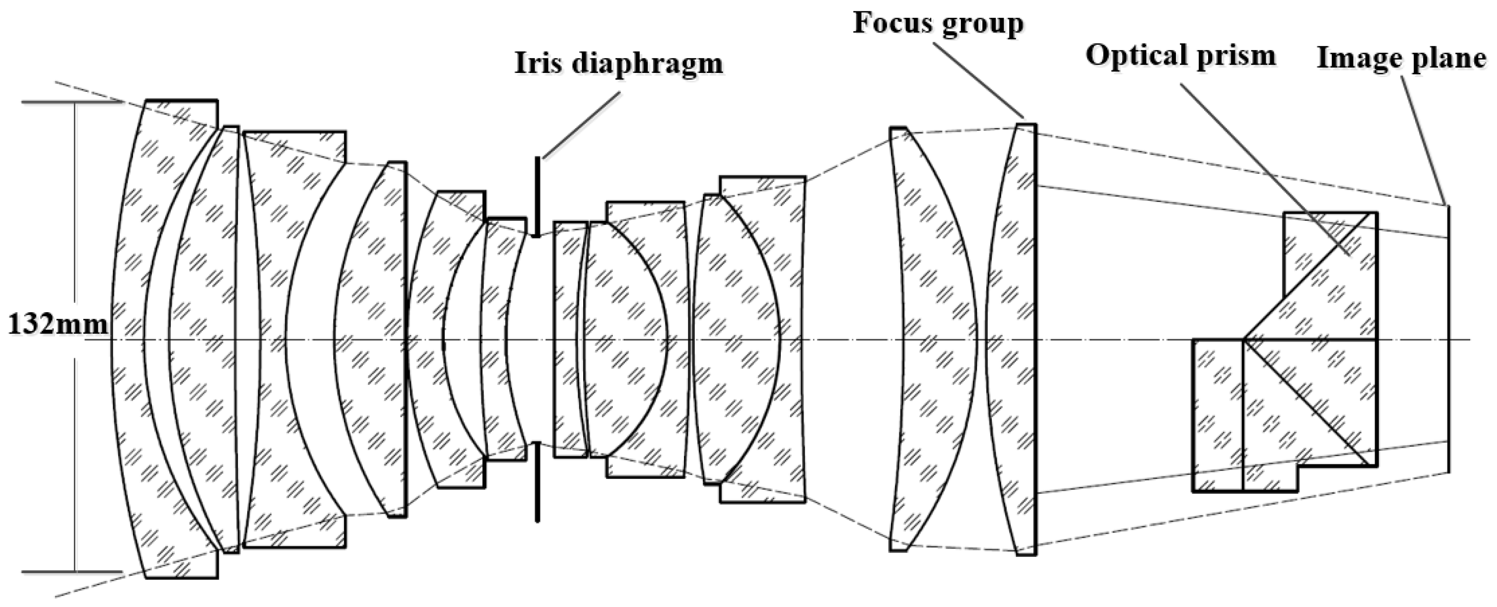
2.2. Optical System
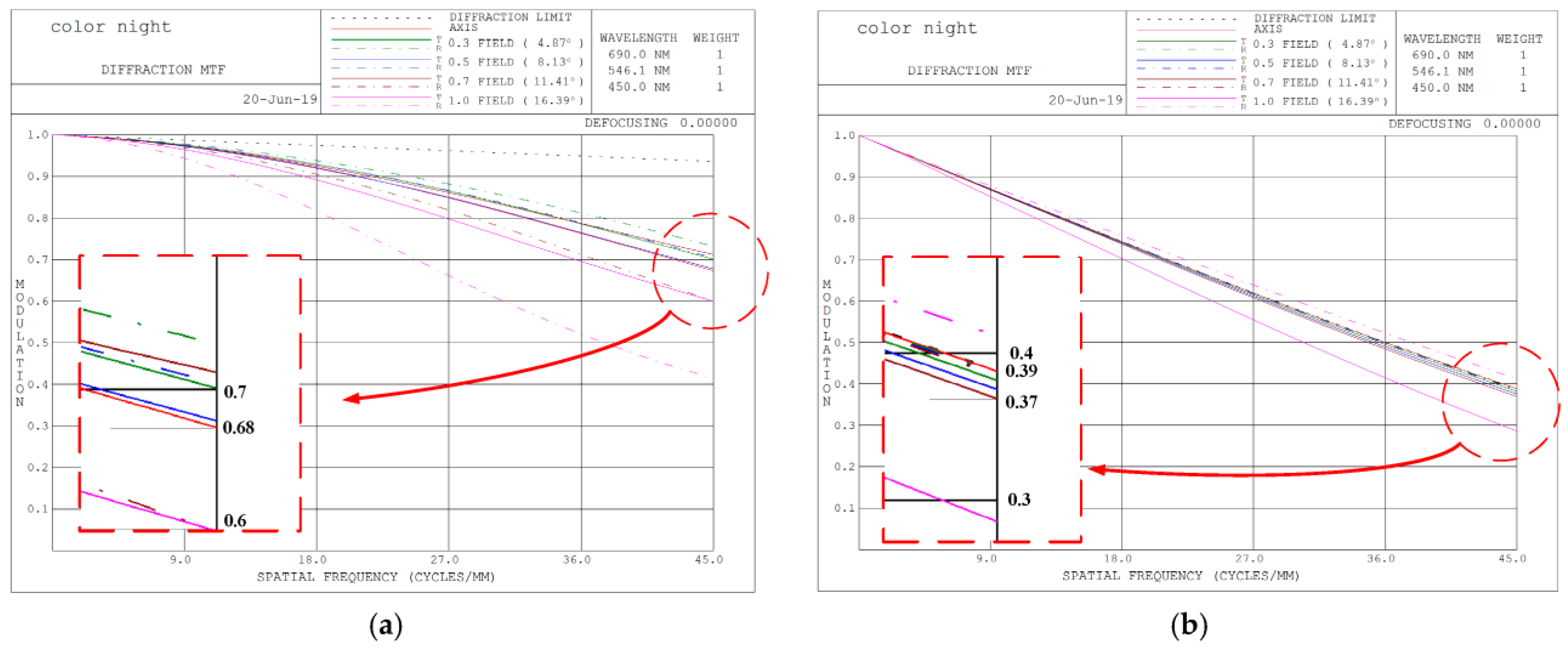
2.3. Imaging Performance Assessment
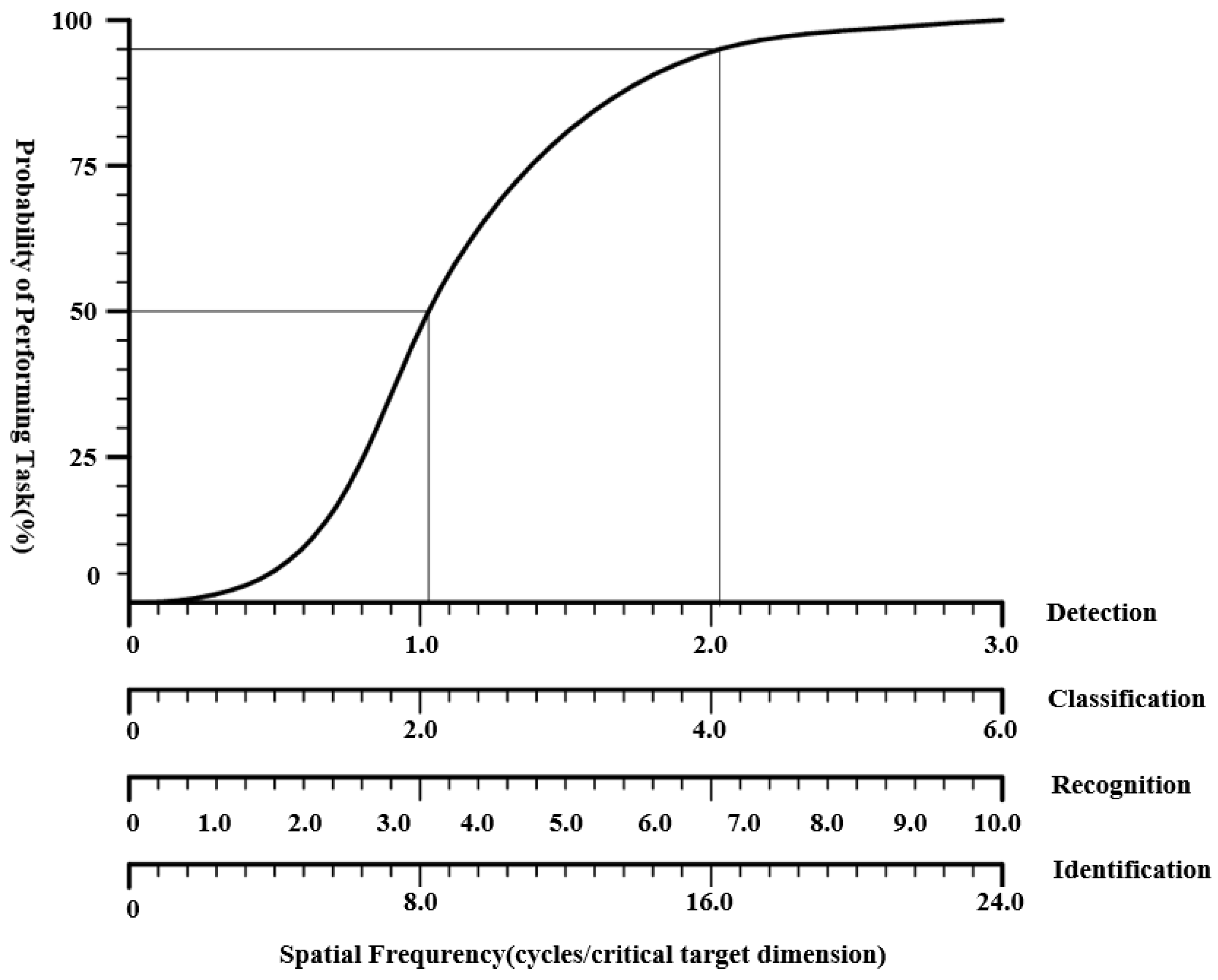
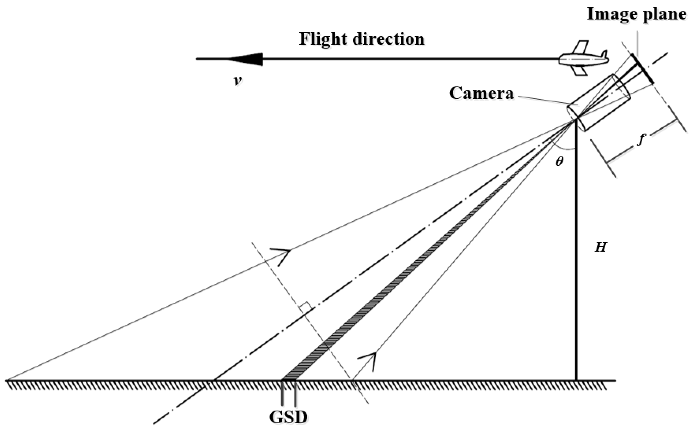
2.3.1. Imaging Distance Estimation
2.3.2. Exposure Time Estimation
2.3.3. Imaging SNR Estimation
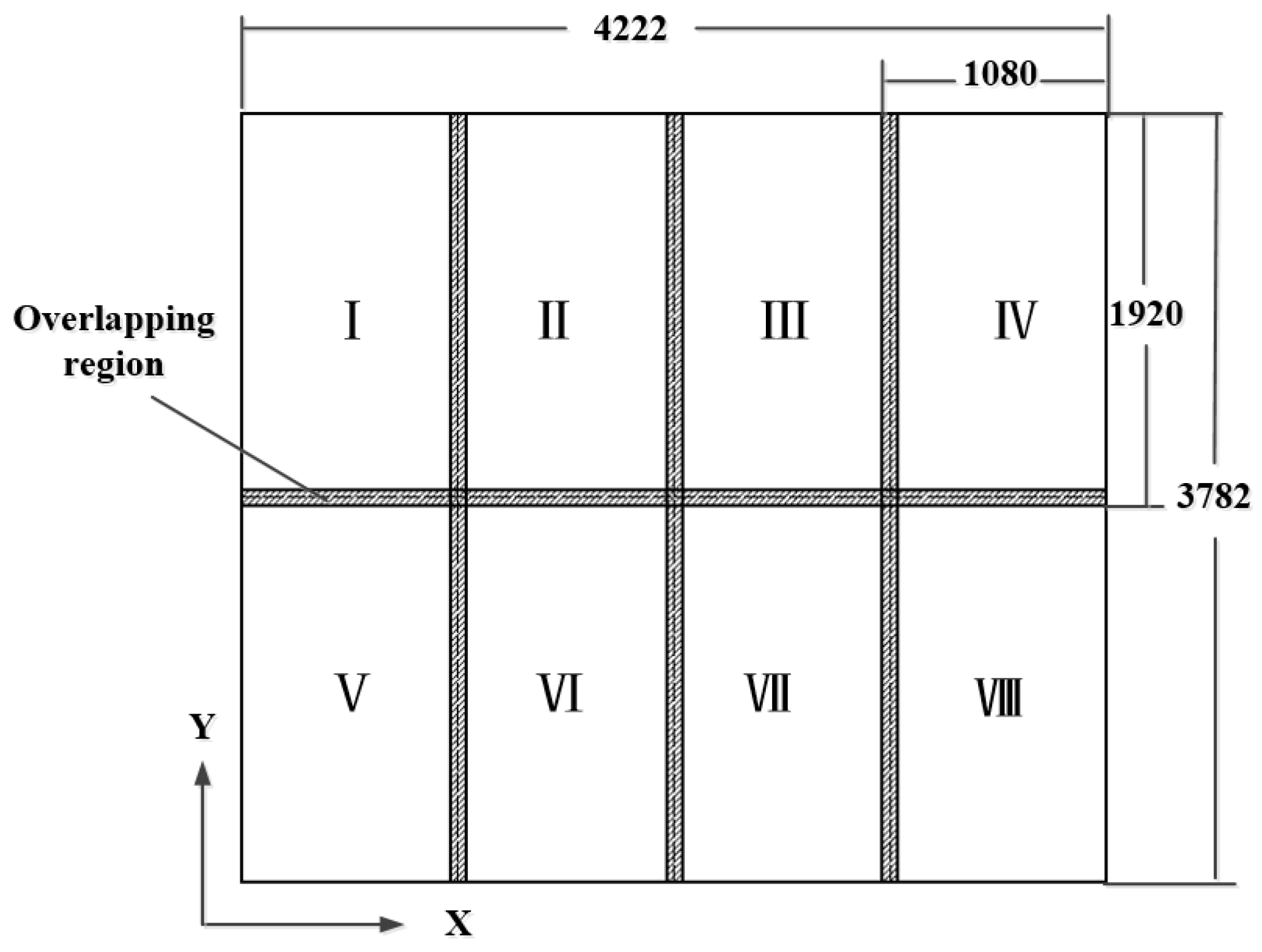
3. Multichannel Optical Butting System Configuration
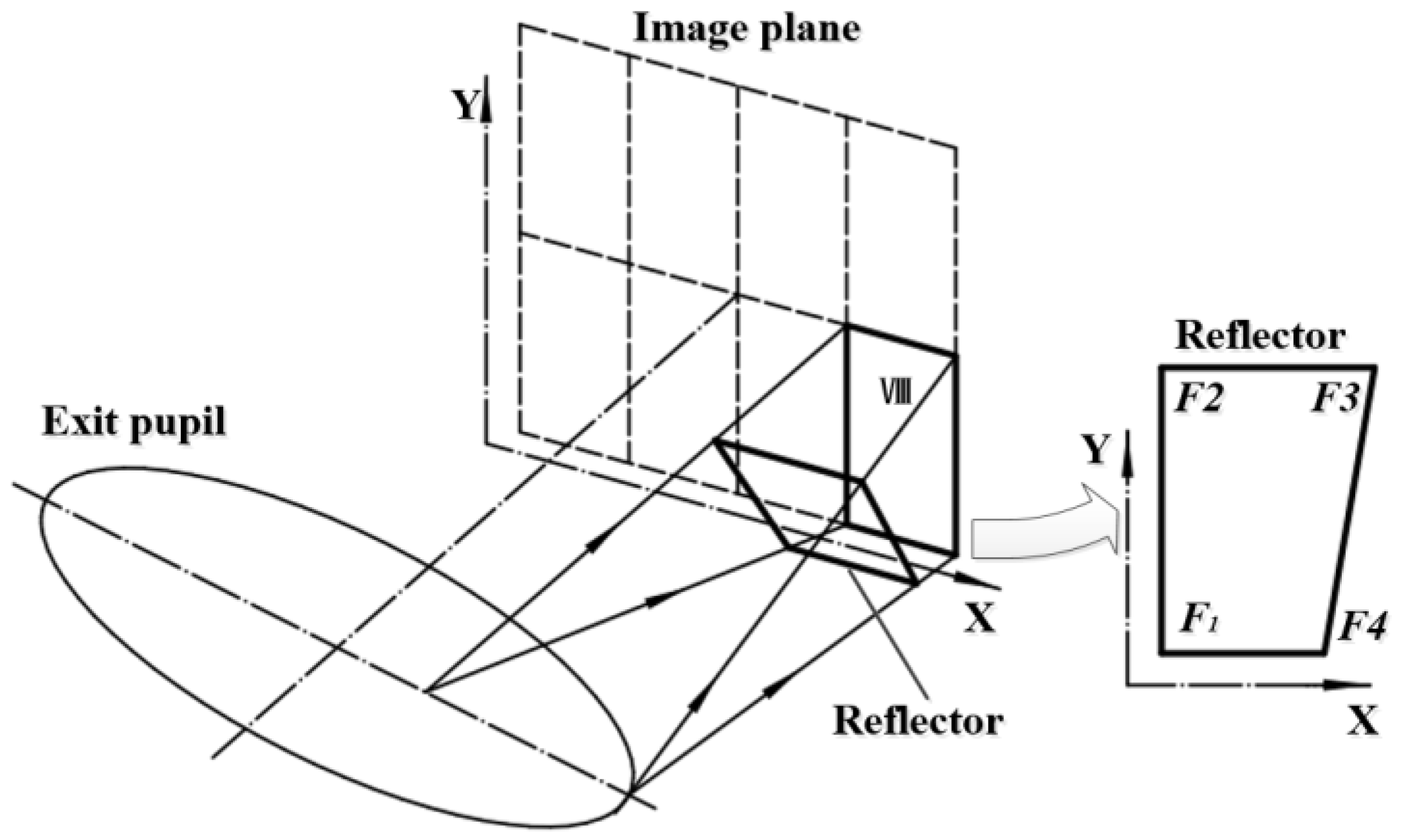
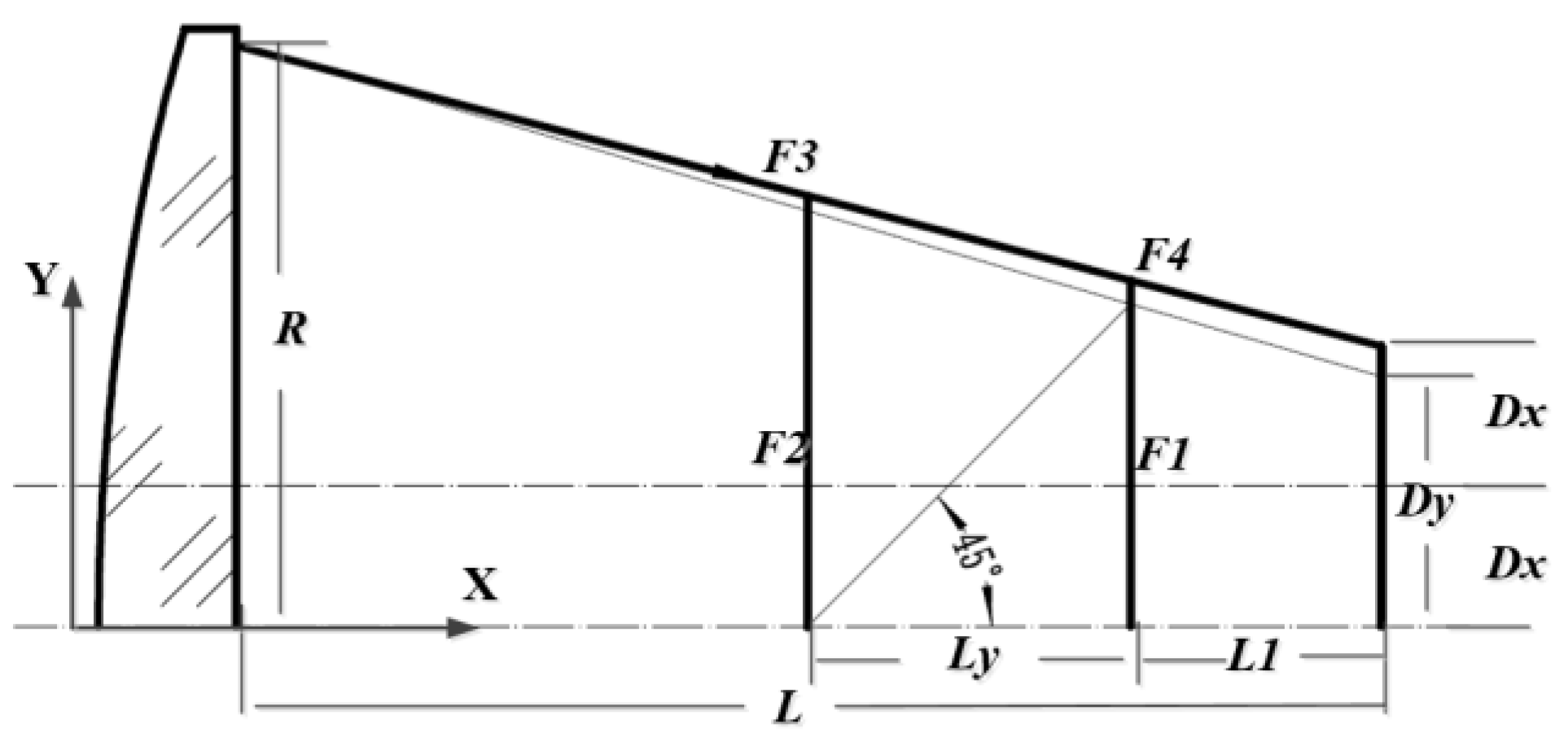
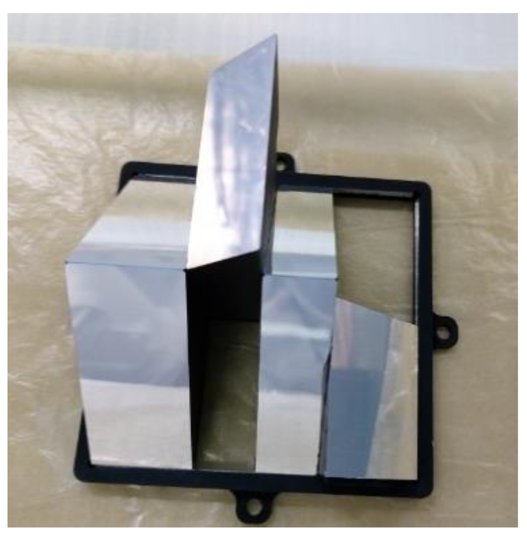
3.1. Optical Butting Reflectors
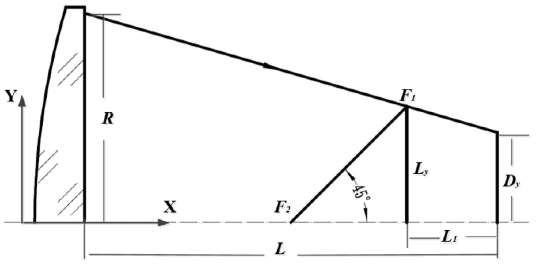
3.2. Calculation of Reflective Prism Parameters
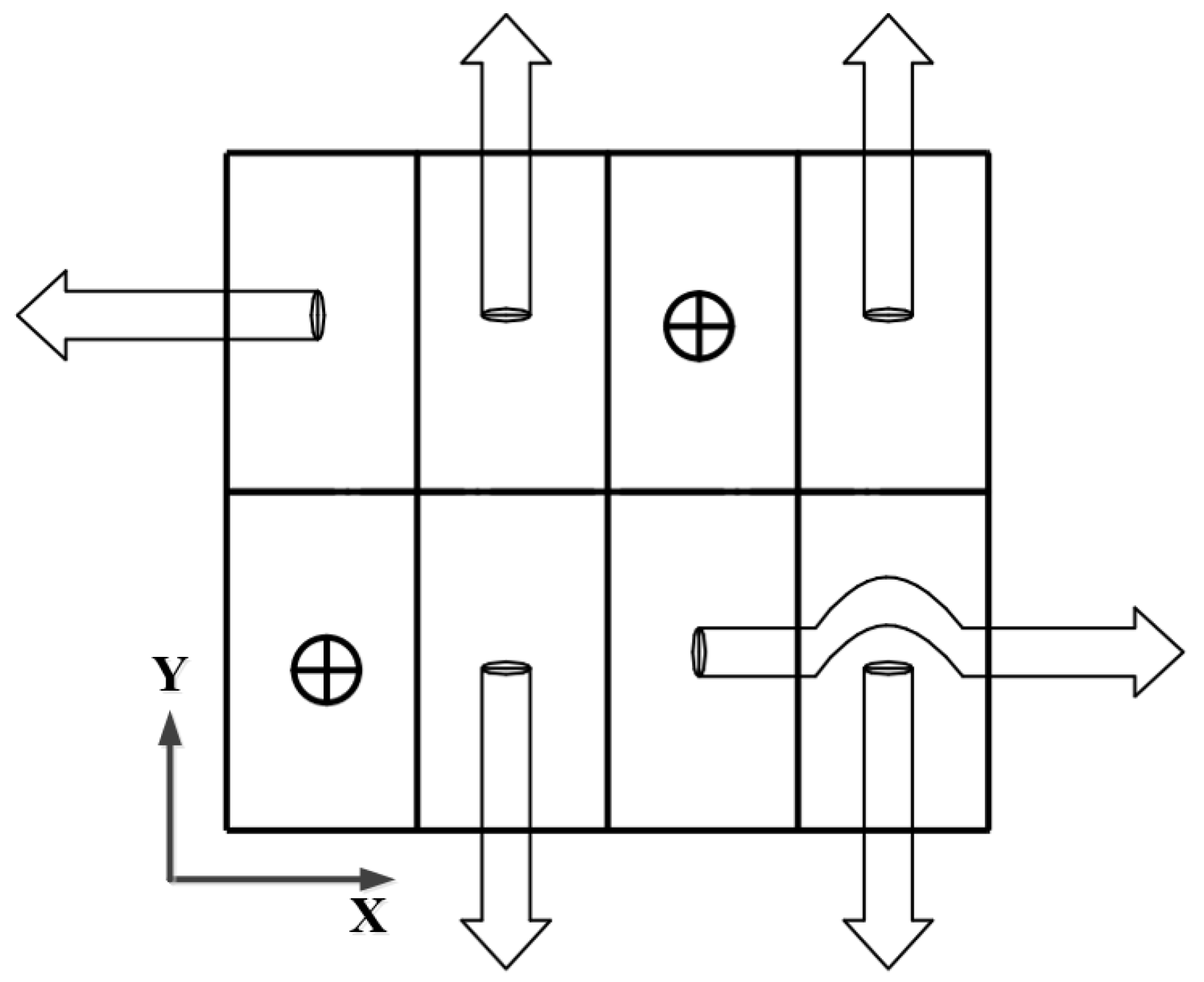
3.3. Mechanical Configuration of the System
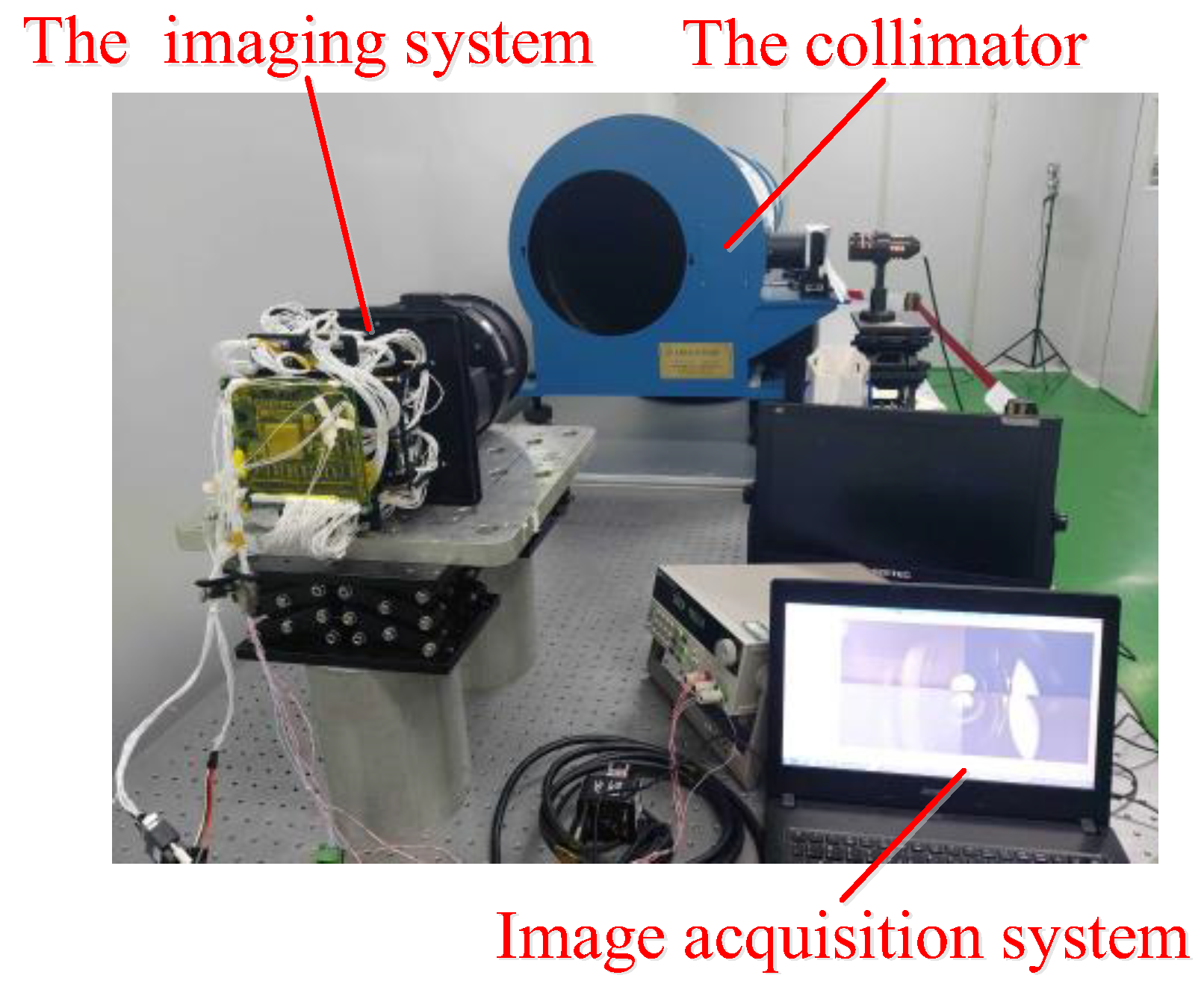
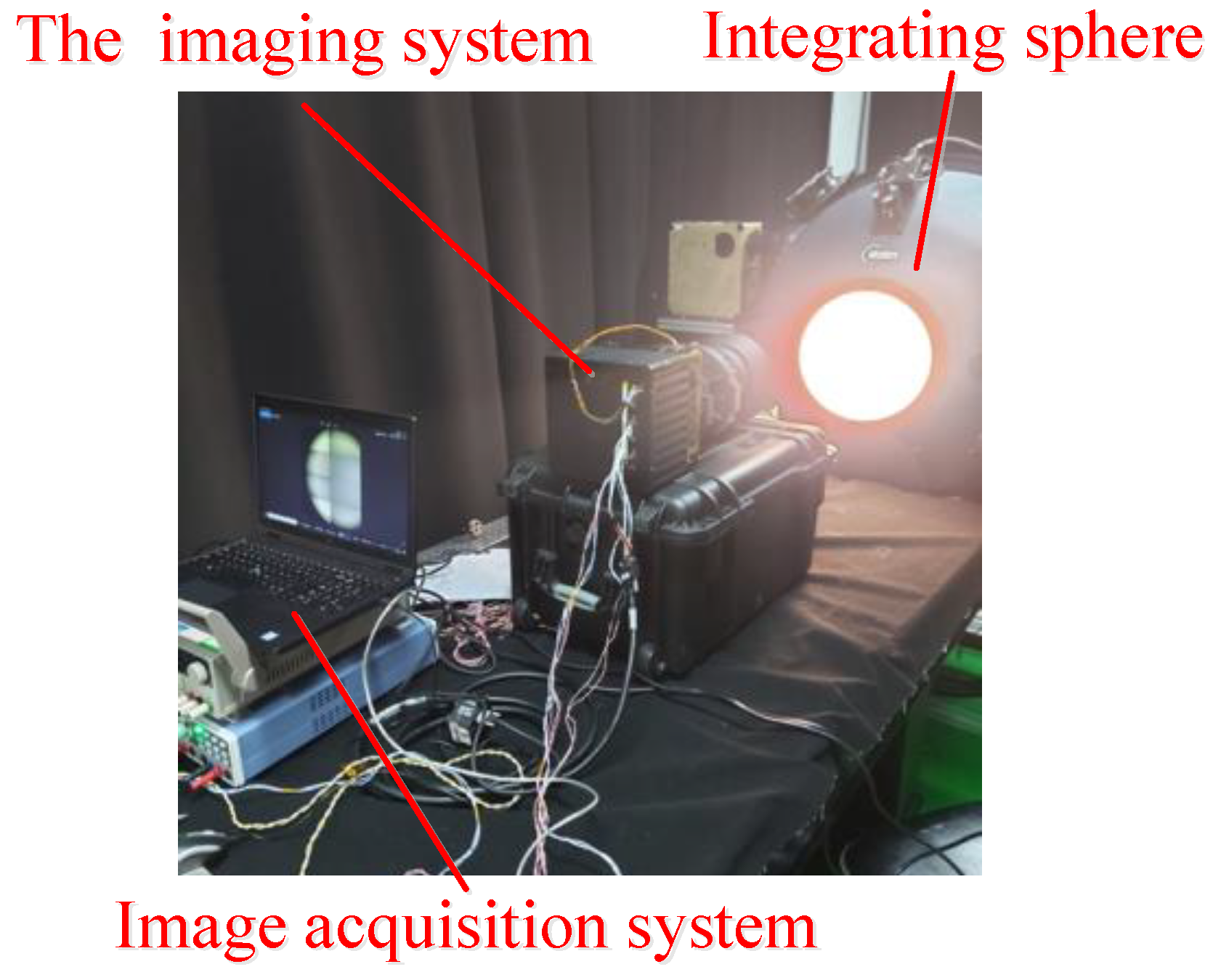
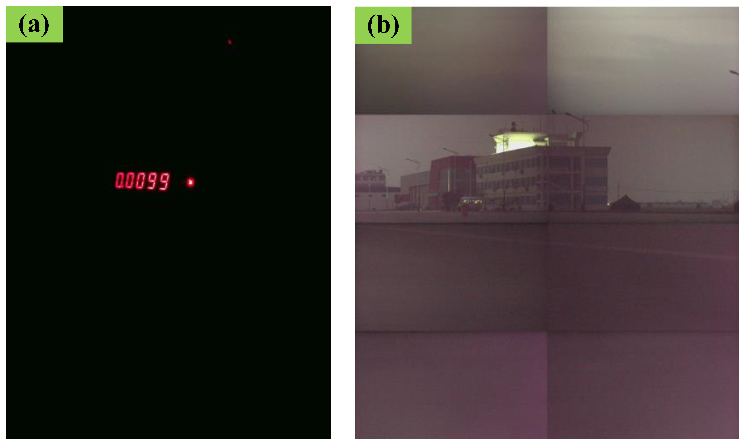
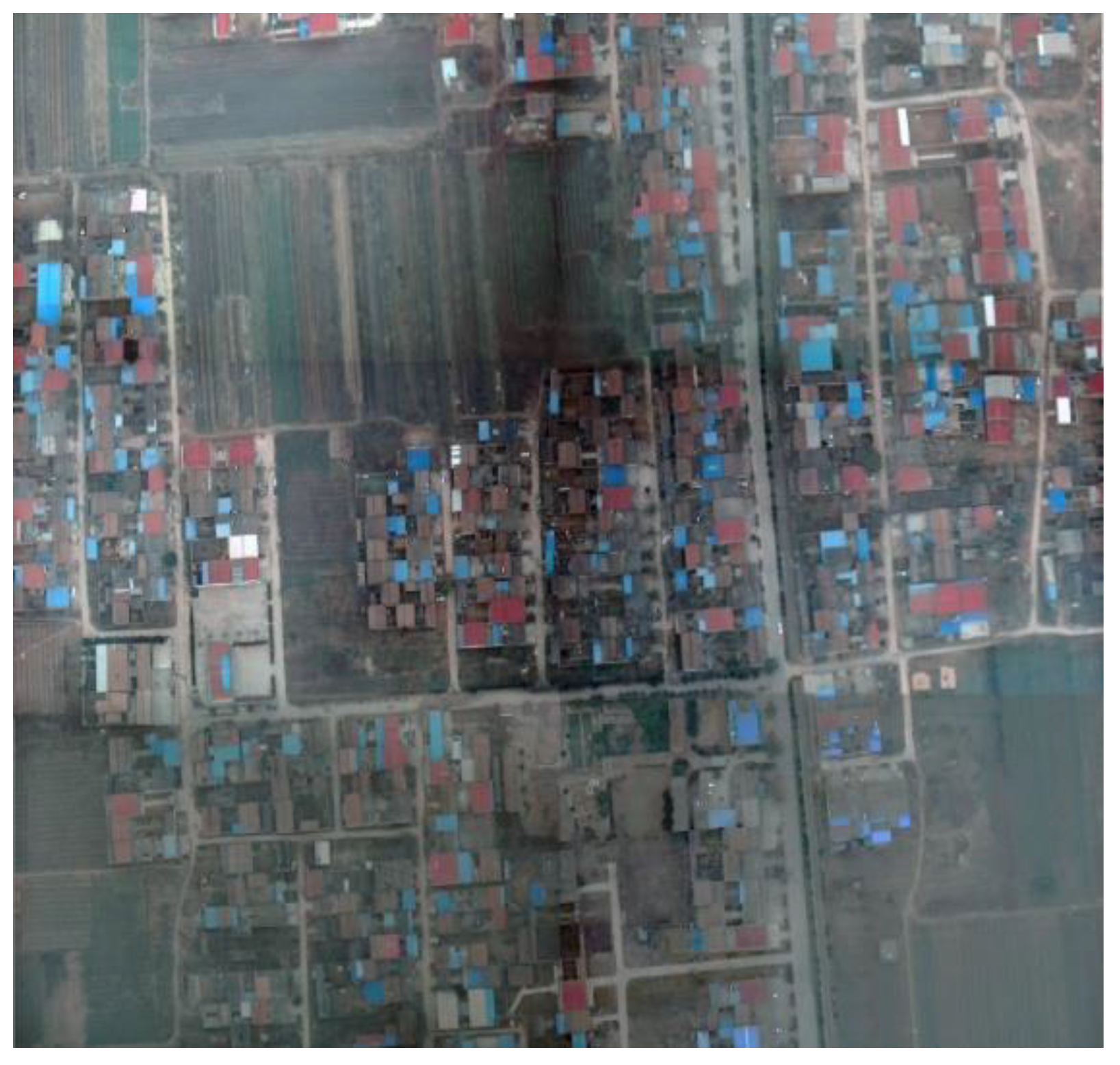
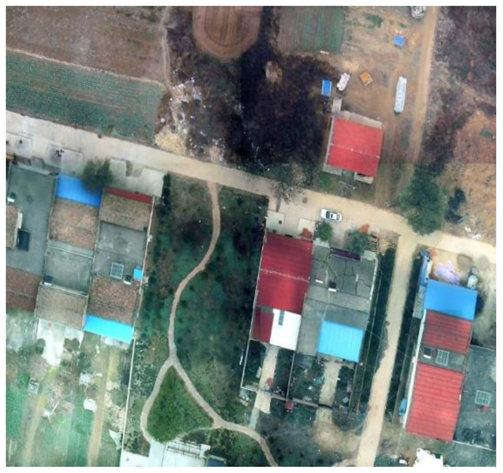
4. Test Results of the System
5. Discussion
Author Contributions
Funding
Institutional Review Board Statement
Informed Consent Statement
Data Availability Statement
Acknowledgments
Conflicts of Interest
References
- Ai, K.-C. Development and prospect of low-light-level(LLL) night vision technology. J. Appl. Opt. 2006, 27, 303–307. [Google Scholar]
- Tian, J.S. New Development of Low Light Level Imaging Sensor Technology. Infrared Technol. 2013, 39, 527–537. [Google Scholar]
- Jin, W.Q.; Wang, L.X.; Zhao, Y.M.; Shi, S.M.; Wang, X. Developments of image processing algorithms for color night vision. Infrared Laser Eng. 2008, 37, 147–150. [Google Scholar]
- Wang, Y.M.; Yang, X.B.; Jin, G.; Xu, W.; Zhang, Z. Study on adaptive exposure time for low-light staring imaging. Acta Photonica Sin. 2016, 45, 75–81. [Google Scholar]
- Sun, Y.; Lou, C.; Jiang, Z.; Zhou, H. Experimental research of representative wavelengths of tricolor for color CCD camera. J. Huazhong Univ. Sci. Technol. 2009, 37, 108–111. [Google Scholar]
- Tang, H.; Zhu, H.; Fei, L.; Wang, T.; Cao, Y.; Xie, C. Low-Illumination Image Enhancement Based on Deep Learning Techniques: A Brief Review. Photonics 2023, 10, 198. [Google Scholar] [CrossRef]
- Liu, Q.; Liu, L.; Deng, Y.; Song, J. Apparent distance theory revision for low-light-level night vision system based on noise factor. Opt. Quantum Electron. 2017, 49, 249. [Google Scholar] [CrossRef]
- Aguilar, M.; Fay, D.A.; Ross, W.D.; Waxman, A.M.; Ireland, D.B.; Racamato, J.P. Real-time fusion of low-light CCD and uncooled IR imagery for color night vision. Enhanc. Synth. Vis. 1998, 3364, 124–135. [Google Scholar]
- Daigle, O.; Djazovski, O.; Laurin, D.; Doyon, R.; Artigau, É. Characterization results of EMCCDs for extreme low-light imaging. High Energy Opt. Infrared Detect. Astron. V 2012, 8453, 10–18. [Google Scholar]
- Lu, C.; Liu, C.; Shao, M.; Wu, Z.; Jiang, C.; Cao, J.; Chen, T. Design and Performance Analysis of the Highly Sensitive Deep Vacuum Cooling sCMOS Imaging System for Highly Sensitive Detection of Space Targets. Photonics 2023, 10, 819. [Google Scholar] [CrossRef]
- Rogalski, A. Progress in focal plane array technologies. Prog. Quantum Electron. 2012, 36, 342–473. [Google Scholar] [CrossRef]
- Shi, L. Research on a Mechanical Interleaving Stitching Method of CCDs for Remote Sensing Camera. Infrared 2009, 30, 12–15. [Google Scholar]
- Meng, Q.H. Optical assembly of area array CCD focal plane for ballistic camera. Ome Inf. 2011, 28, 46–49. [Google Scholar]
- Wu, H.; Tao, S.; Zhang, L.; Zhang, J. Tricolor acquisition and true color images fusion method under low illumination condition. J. Appl. Opt. 2016, 37, 673–679. [Google Scholar]
- Tang, X.; Yao, L. Design of optical filters for three primary colors. Laser Technol. 2014, 38, 274–277. [Google Scholar]
- Kose, T.; Ben-Mrad, R. Optical design of a 2× zoom lens for miniature imaging systems. Opt. Eng. 2019, 58, 085107. [Google Scholar] [CrossRef]
- Mann, A. Developments and trends in infrared zoom lenses from 2000 to 2010. Opt. Eng. 2013, 52, 013001. [Google Scholar] [CrossRef]
- Kuo, C.W.; Lin, C.L.; Han, C.Y. Dual field-of-view midwave infrared optical design and athermalization analysis. Appl. Opt. 2010, 49, 3691–3700. [Google Scholar] [CrossRef]
- Qian, X.; Wang, Y.; Wang, B. Effective contrast enhancement method for color night vision. Infrared Phys. Technol. 2012, 55, 130–136. [Google Scholar] [CrossRef]
- Hynecek, J.; Nishiwaki, T. Excess noise and other important characteristics of low light level imaging using charge multiplying CCDs. IEEE Trans. Electron Devices 2003, 50, 239–245. [Google Scholar] [CrossRef]
- Chen, X.; Lv, Q. Microbolometric theoretical output responsivity analysis for focal plane array. Opt. Eng. 2015, 54, 63105. [Google Scholar] [CrossRef]
- Liu, B.; Zhou, B.; Gao, Z.; Zhang, W. Research on testing output signal-to-noise ratio of image intensifier. Opt. Des. Test. II 2005, 5638, 605–612. [Google Scholar]
- Jorden, P.R.; Morris, D.G.; Pool, P.J. Technology of large focal planes of CCDs. Proc. SPIE-Int. Soc. Opt. Eng. 2004, 5167, 72–82. [Google Scholar]
- Li, F.; Zhang, X.; Cai, W.; Chang, J.; Gao, L. Parameter Calculation of Splitting Mirrors in Optical-Butting Focal Plane. Acta Opt. Sin. 2020, 40, 1308001. [Google Scholar]
- Jia, X.Z.; Jin, G. Design and Precision measurement of TDICCD Focal Plane for Space Camera. In Proceedings of the 6th International Symposium on Advanced Optical Manufacturing and Testing Technologies: Optoelectronic Materials and Devices for Sensing, Imaging, and Solar Energy, Xiamen, China, 15 October 2012. [Google Scholar]
- LI, Z.; Wang, Z.; Wu, K. Optical assembly of CCD focal plane for space camera. Opt. Precis. Eng. 2000, 8, 213–216. [Google Scholar]
- Guo, J.; Gong, D.; Zhu, L.; Sun, J.; Shao, M. Calculation of overlapping pixels in interleaving assembly of CCD focal plane of mapping camera. Opt. Precis. Eng. 2013, 21, 1251–1257. [Google Scholar]
- Marks; Daniel, L. Close-up imaging using microcamera arrays for focal plane synthesis. Opt. Eng. 2011, 50, 33205. [Google Scholar] [CrossRef]
- Qian, X.; Han, L.; Wang, Y.; Wang, B. Color contrast enhancement for color night vision based on color mapping. Infrared Phys. Technol. 2013, 57, 36–41. [Google Scholar] [CrossRef]


| Project | Index |
|---|---|
| Focus | 131 mm |
| FOV angle | 24.6° × 21.8° |
| F-number | 1.6~20 |
| Operating waveband | 435 nm~656 nm |
| MTF@40 lp/mm | ≥0.40 |
| Distortion | ≤2.2% |
| Back focal length | 105 mm |
| Parameter | Value |
|---|---|
| Active array size | 1920 × 1080 |
| Pixel size | 13 × 13 μm |
| Full well capacity | 45 Ke |
| Peak QE | 55% |
| Read noise | 1.5e (RMS) |
| Dark current | 5e/pixel/s@20 °C |
| Dynamic range | 65 dB |
| Flight Height | Imaging Pixel Number | Imaging Line Pair Number | Surveillance Level | Probability |
|---|---|---|---|---|
| 5 km | 8 × 12 | 4 × 6 | Recognition | ≥50% |
| 10 km | 4 × 6 | 2 × 3 | Detection | ≥90% |
| 15 km | 3 × 4 | 1 × 2 | Detection | ≥50% |
| Flight Height | Flight Velocity | Viewing Method | Maximum Exposure Time |
|---|---|---|---|
| 5 km | 200 km/h | Vertical downward view | 4.5 ms |
| 2 km | 200 km/h | Oblique viewing of a target at a distance of 5 km | 11.2 ms |
| 1 km | 200 km/h | Oblique viewing of a target at a distance of 5 km | 22.5 ms |
| Illuminance (Lux) | SCMOS No. | I | II | III | IV | V | VI | VII | VIII |
|---|---|---|---|---|---|---|---|---|---|
| 0.01 | Gray value | 113.3 | 95.1 | 101.8 | 124.4 | 117.0 | 103.3 | 92.8 | 128.8 |
| 10,000 | Gray value | 786.2 | 520.5 | 613.3 | 811.1 | 659.6 | 580.8 | 533.2 | 850.5 |
Disclaimer/Publisher’s Note: The statements, opinions and data contained in all publications are solely those of the individual author(s) and contributor(s) and not of MDPI and/or the editor(s). MDPI and/or the editor(s) disclaim responsibility for any injury to people or property resulting from any ideas, methods, instructions or products referred to in the content. |
© 2024 by the authors. Licensee MDPI, Basel, Switzerland. This article is an open access article distributed under the terms and conditions of the Creative Commons Attribution (CC BY) license (https://creativecommons.org/licenses/by/4.0/).
Share and Cite
Peng, J.; Yang, H.; Lei, Y.; Yu, W.; Chen, W.; Zhang, G. Design of an Airborne Low-Light Imaging System Based on Multichannel Optical Butting. Photonics 2024, 11, 636. https://doi.org/10.3390/photonics11070636
Peng J, Yang H, Lei Y, Yu W, Chen W, Zhang G. Design of an Airborne Low-Light Imaging System Based on Multichannel Optical Butting. Photonics. 2024; 11(7):636. https://doi.org/10.3390/photonics11070636
Chicago/Turabian StylePeng, Jianwei, Hongtao Yang, Yangjie Lei, Wanrong Yu, Weining Chen, and Guangdong Zhang. 2024. "Design of an Airborne Low-Light Imaging System Based on Multichannel Optical Butting" Photonics 11, no. 7: 636. https://doi.org/10.3390/photonics11070636
APA StylePeng, J., Yang, H., Lei, Y., Yu, W., Chen, W., & Zhang, G. (2024). Design of an Airborne Low-Light Imaging System Based on Multichannel Optical Butting. Photonics, 11(7), 636. https://doi.org/10.3390/photonics11070636