Abstract
Quantum dot light-emitting diodes (QLEDs) hold great promise for next-generation display applications owing to their exceptional optical properties and versatile tunability. In this study, we investigate the effects of quantum dot (QD) shell thickness, polyethylenimine (PEI) concentration, and PEI layer position on the performance of inverted QLED devices. Two types of alloyed-core/shell QDs with varying shell thicknesses were synthesized using a one-pot method with mean particle sizes of 8.0 ± 0.9 nm and 10.3 ± 1.3 nm for thin- and thick-shelled QDs, respectively. Thick-shelled QDs exhibited a higher photoluminescence quantum yield (PLQY) and a narrower emission linewidth compared to their thin-shelled counterparts. Next, QLEDs employing these QDs were fabricated. The incorporation of PEI layers on either side of the QD emissive layer significantly enhanced device performance. Using PEI on the hole transport side resulted in greater improvement than on the electron injection side. Sandwiching the QD layer between two PEI layers led to the best performance, with a maximum external quantum efficiency (EQE) of 17% and a peak luminance of 91,174 cd/m2 achieved using an optimized PEI concentration of 0.025 wt% on both electron injection and hole injection sides. This study highlights the critical role of QD shell engineering and interfacial modification in achieving high-performance QLEDs for display applications.
1. Introduction
Ever since their first demonstration in the 1980s [1], the unique properties of QDs, with their capacity for improving colloidal optoelectronics, have aroused considerable interest among researchers. By directly tuning the physical dimensions through facile synthetic procedures, precise control can be exerted over QD behavior, granting them with characteristics ideal for a range of advanced applications. Specifically, the quantum confinement effect allows size-dependent bandgap engineering and achievement of emission wavelengths across the visible and infrared spectra, in addition to exceptionally high, up-to near-unity quantum yields [2,3]. These exceptional optical qualities, along with the ability to manipulate properties through structural modifications, underpin the diverse technological capabilities of QDs. They have shown promise in areas including displays, photovoltaics, biological imaging, and sensing, with emerging use cases like quantum computing also on the horizon [4,5,6,7,8].
QD technologies have attracted significant commercial attention in recent years especially for display applications that have been an area generating substantial industry focus and investment [9]. Displays incorporating QDs utilize either photoluminescence or electroluminescence phenomena. In the former case, QDs act as color-converters, while in the latter case, QDs become self-emissive through exciton recombination [10]. QLEDs in particular demonstrate promise as an electroluminescent technology for displays, offer several key performance advantages, including high contrast ratios, broad color gamut exceeding NTSC recommendations, high energy efficiencies, low production costs compliant to scaling, thin form factors, and compatibility with flexible substrates [11,12,13].
New-generation flat panel display technologies employ active-matrix-control mechanism to address individual pixels. Unlike LCD displays where TFT matrix trigger voltage to modulate individual pixels, they provide current to control pixels in self-emissive OLED and QLED displays through power line. Amorphous silicon (a-Si) is the mostly used material for TFT backplanes in the industry due to its cost advantage, manufacturing simplicity, good scalability, and satisfactory performance [14]. The bottom cathode can directly connect to the TFT located at the drain end of an a-Si TFT backplane. This makes the gate and source voltages of the driving TFT independent of the QLED operation [15]. Therefore, the utilization of an inverted QLED architecture, where indium–tin oxide (ITO) functions as the cathode, significantly enhances the applicability of QLED devices for displays.
The polyethyleneimine, branched or ethoxylated (PEI or PEIE), layer acts as an effective interfacial energy level modification agent between charge transport/injection and emissive layers. It facilitates electron injection from the cathode into the quantum dots. This helps improve device efficiency and performance. The amine groups in PEI and PEIE can also reduce the work function of cathode materials like ITO [16]. This better matches the cathode work function with the adjacent electron injection layer and enables more efficient charge injection. The PEI or PEIE layer can passivate or stabilize the surface of metal oxide layers like ZnO that are commonly used in inverted QLED architectures [17,18,19]. This enhances the interfacial properties and improves device stability.
When PEI is employed between the QD and poly(9-vinylcarbazole) (PVK) layers, it facilitates the formation of dipoles, which effectively reduces the vacuum level and promotes improved hole injection. Furthermore, PEI has been demonstrated to passivate surface defects on the QDs. However, due to the insulating nature of PEI, an excessive layer thickness can hinder hole injection, resulting in a deterioration of device performance [20]. Furthermore, research shows the PEI layer provides a more uniform surface compared to PEIE, which showed some aggregation. The morphology of the interlayer impacts charge transport properties [21].
At elevated current densities in QLEDs, the presence of multiple excitons within a single QD becomes a commonplace scenario. Given the considerably higher rates of Auger processes compared to radiative processes, QDs in multi-exciton states readily undergo deexcitation through nonradiative Auger processes [22,23]. Suppression of Auger recombination emerges as a crucial strategy for enhancing the overall performance of QLED devices. Substantial progress has been made in this regard, with research indicating that QDs featuring abrupt confinement potentials exhibit more efficient Auger recombination than those with softer confinement potentials. The mitigation of confinement potential irregularities can be achieved through the creation of an alloyed interface at the core/shell junction [24,25]. The findings emphasize the significance of controlling Auger recombination dynamics for optimizing the performance of QLEDs.
Optimization of the shell thickness in alloyed-core/shell QDs has been performed comprehensively in the past, because this highly affects their optical and electronic properties. With an increase in shell thickness, quantum yield generally improves due to better surface passivation, and stability is improved due to reduced nonradiative recombination [26,27,28,29,30]. Moreover, single QDs with thicker shells were found to suppress the effect of blinking, a key factor in bioimaging applications [31,32]. However, the advantages of the increase in the thickness of shells are limited. If the thickness ranges beyond an optimum value, it will then relax by causing strain at the core–shell interface, generating defects that may diminish quantum yield [33,34]. Also, very thick shells may be associated with efficiency roll-off, in which the quantum yield decreases due to increased nonradiative recombination pathways and increased energy barrier for charge injection [35,36]. Therefore, the optimum shell thickness must be properly tuned, balancing the improved performance against the possible drawbacks, according to various applications and QD compositions.
In this study, as the first demonstration, we investigate the QD shell thickness effect on the inverted QLED devices in combination with the PEI concentration and position. Contrary to some claims that the insulating nature of PEI slowed down electrons to improve the charge balance on the active layer, using PEI on the hole side resulted in higher improvement. After showing the superior performance of thick-shelled QDs in the configuration of the PEI layer on both sides of the QD layer, PEI concentration optimization on the best performing device architecture was carried out. As a result, the maximum EQE of 17% and the maximum luminance of 91,174 cd/m2 were achieved.
2. Materials and Methods
2.1. Materials
Zinc acetate dihydrate (Zn(OAc)2·2H2O, 99.999%), cadmium oxide (CdO, 99.99%), selenium (Se, 99.99%), sulfur (S, 99.998%), oleic acid (OA, 90% technical grade), 1-octadecene (ODE, 90% technical grade), trioctylphosphine (TOP, 90% technical grade), tetramethylammonium hydroxide pentahydrate(TMAH, 97%), ethanolamine (98%), dimethyl sulfoxide (DMSO), poly(9-vinylcarbazole) (PVK, average Mw ≈ 1,100,000), and polyethylenimine (PEI, Mw ≈ 800 g/mol) were purchased from Sigma-Aldrich. PEDOT:PSS solution branded as Clevios™ P VP AI 4083 was purchased from Ossila, Sheffield, UK.
2.2. Quantum Dot Synthesis
Thin-shelled QDs were synthesized with some modifications made to the procedure reported in the literature [30]. Briefly, 0.25 mmol CdO, 3.41 mmol Zn(OAc)2·2H2O, and 7 mL OA were placed in a round-bottom flask. The mixture was heated up to 150 °C under nitrogen flow and degassed for 1 h. A 15 mL volume of ODE was added and degassed for 30 min at 90 °C down to 20 mTorr pressure. Temperature was raised to 290 °C, and then, a mixture of 2.1 mmol Se, 2.5 mmol S, and 2.65 mL TOP was swiftly injected. The temperature was raised to 310 °C, and after 10 min from the injection, the reaction was cooled down to room temperature for purification.
Thick-shelled QDs were synthesized by continuing with the swift injection of a solution of 1.6 mmol S in 2.4 mL ODE instead of cooling down. After 10 min, 5 mL zinc oleate solution prepared by mixing 5.72 mmol Zn(OAc)2·2H2O, 6 mL ODE, and 2 mL OA was injected at a rate of 0.6 mL/min. Subsequently, a solution of 3 mmol S, 0.6 mL OA, and 2.4 mL ODE was injected at the same rate. The shell was allowed to form for 20 min. Lastly, 2 mL zinc oleate solution was injected at 1 mL/min rate. After 10 min, the reaction was cooled to room temperature. QD purification was performed via centrifugation in excess acetone and methanol at 5000 rpm for 10 min. QDs were redispersed in n-hexane, and precipitation was repeated two more times. Finally, QDs were dispersed in octane at a concentration of 20 mg/mL.
2.3. ZnO Nanoparticle Synthesis
ZnO nanoparticles were synthesized following a recipe from the literature with some modifications [17]. In a 100 mL volumetric flask, 3 mmol Zn(OAc)2·2H2O and 30 mL dried DMSO were placed. Separately, 5.6 mmol TMAH was dissolved in 10 mL ethanol inside an argon-filled glovebox. After the complete dissolution of Zn(OAc)2·2H2O, the TMAH solution was introduced into the flask at 1 mL/min rate. The reaction was allowed to take place for 24 h. Then, ZnO nanoparticles were precipitated via centrifugation in excess ethyl acetate. Ethanolamine was used at 1:20 ratio in ethanol to redisperse ZnO NPs. After repeating the same precipitation step, ZnO NPs were redispersed in ethanol at a 30 mg/mL concentration.
2.4. Device Fabrication
QLEDs were fabricated on pre-patterned indium–tin oxide-coated glass substrates (20 Ω/square sheet resistance and 4.5 mm2 active area). The substrates were cleaned by ultrasonication successively in 0.1% Hellmanex III-de-ionized (DI) water solution, hot DI water, and isopropanol. Lastly, all substrates were treated with air plasma for 10 min before transferring them into an argon-filled glovebox. The ZnO layer was coated (30 mg/mL, ethanol) at 2000 rpm for 60 s and annealed at 110 °C for 20 min. QD nanoparticles were deposited (20 mg/mL, octane) at 3000 rpm for 40 s, followed by annealing at 100 °C for 10 min. The PEI solution in ethoxyethanol was formed by spin-coating at 3000 rpm for 60 s. After annealing at 100 °C for 20 min, the PVK layer was deposited from its 6 mg/mL chloroform solution at 4500 rpm for 60 s and annealed at 100 °C for 20 min. Lastly, PEDOT:PSS solution was diluted with 2-propanol at 1:1 ratio to improve the film quality on the hydrophobic PVK layer and coated at 4500 rpm for 60 s. Then, the formed film was annealed at 100 °C for 15 min. Finally, the anode was formed by the thermal evaporation of Al (100 nm) through a shadow mask under high vacuum (~4 × 10⁻⁶ Torr). All devices were packed with UV-curable epoxy and encapsulation coverslips (~0.5 mm thick) before being exposed to ambient environment.
2.5. Characterizations
TEM images were taken using FEI TALOS F200S. X-ray diffraction (XRD) patterns were collected with Bruker D8 DISCOVER. The absorbance and PL spectra were measured by Genesys 10S UV-Visible spectrophotometer and Cary Eclipse 9800A fluorescence spectrometer, respectively. Time-resolved photoluminescence (TRPL) experiments were conducted using the PicoQuant Fluo Time 200 time-correlated single-photon counting (TCSPC) system, which was coupled with a laser excitation source emitting light at 371 nm and operated at a repetition rate of 5 MHz with 0.13 mW max optical power at this frequency. The Time Harp 260 PICO system was used to gather the lifetimes of the samples. To analyze the data, decay curves were constructed, and the average lifetimes were calculated by fitting the data with a two-exponential model using the FluoFit software (version 4.6.6.0) developed by PicoQuant Technologies. PLQY measurements were taken with Hamamatsu C11347 absolute PL quantum yield spectrometer. All optoelectronic data on QLEDs were collected by Hamamatsu PMA-12 Photonic multichannel analyzer coupled with an integrating sphere and Keithley 2400 source meter.
3. Results and Discussion
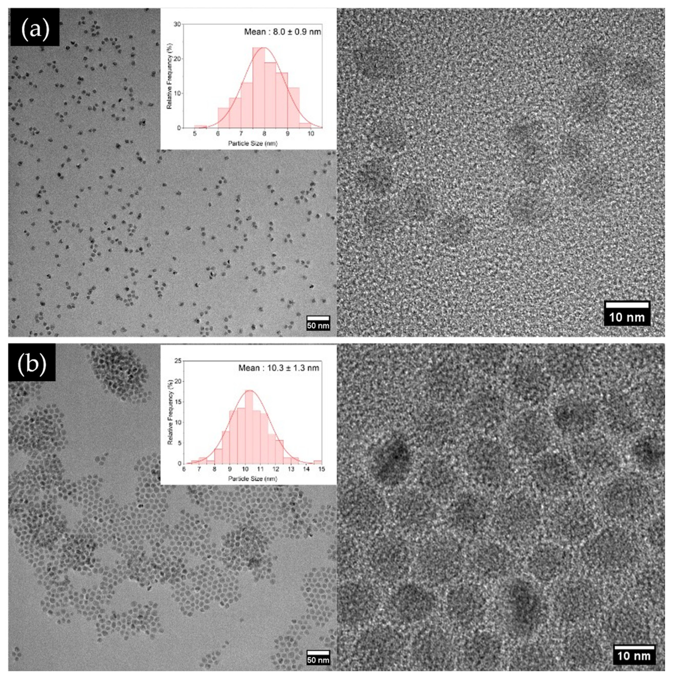
To understand the effect of the shell thickness, we synthesized two different QDs grown on the same platform by employing a one-pot synthesis technique [30]. QDs synthesized in this study both consists of CdSe@ZnS alloyed core/shell and additional ZnS shell for thick-shelled QDs. One type of the QDs employed a relatively thin ZnS shell, whereas another one included a significantly thicker shell. Additional ZnS growth was carried to obtain these thick-shelled nanocrystals, which is delineated in the synthesis part. This multi-shell approach is also used for the localization of charge carriers when the monolayer of different semiconductor types are coated repetitively [37]. TEM images in Figure 1 show that the mean particle sizes are 8.0 ± 0.9 nm and 10.3 ± 1.3 nm for thin- and thick-shelled QDs, respectively. Additional ~1.2 nm shell coating corresponds to ~4 monolayers of ZnS [38].

Figure 1.
TEM images of (a) thin- and (b)thick-shelled QDs. Scale bars are 50 and 10 nm in length, respectively. Insets show the particle size histogram.
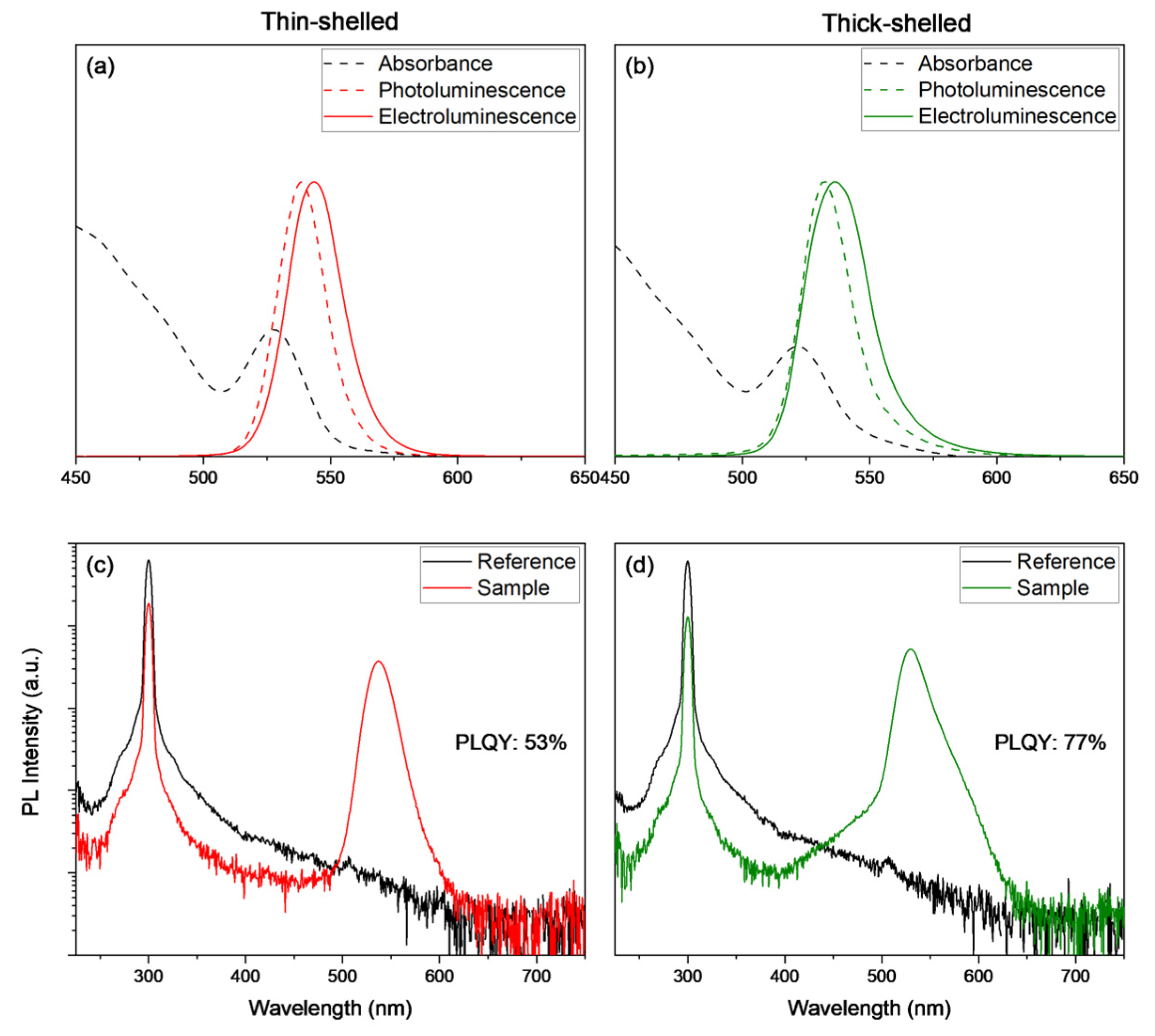
Optical characterizations of these samples are shown in Figure 2. The emission wavelengths of synthesized QDs are 539 and 533 nm for thin- and thick-shell samples, respectively. Owing to their monodispersity, both types of QDs achieve similar linewidths, which are 22.1 nm for the thick-shelled QDs and 22.7 nm for the thin-shelled QDs. On the other hand, additional shelling process resulted in 45% increase in PLQY for thick-shelled QD and reached 77.2%, whereas the PLQY of the thin-shelled QD remains at 53%. These high-quantum yield observations can be explained by two concurrent effects. The first is due to the confinement of electron and hole wavefunctions in the core, thereby increasing their recombination probability in the core. The second is the reduction in nonradiative-decay probability occurring at surface states. It is therefore the combination of these two phenomena which gives rise to a dramatic improvement in the photoluminescence quantum yield of the QDs as shown in the literature [39].

Figure 2.
(a,b) Absorbance, photoluminescence, electroluminescence, and (c,d) absolute PLQY measurement spectra of thin- and thick-shelled QDs, respectively.
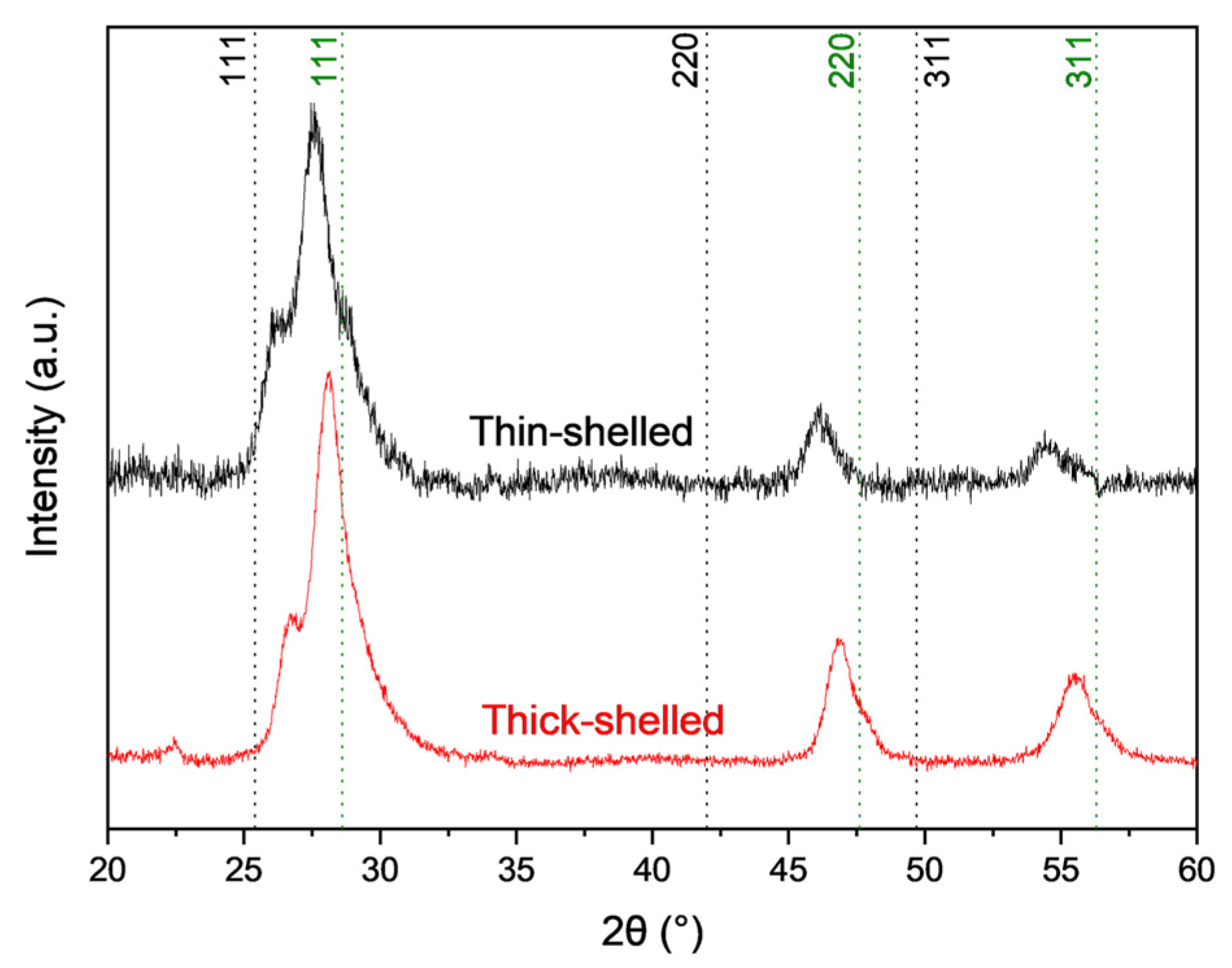
To gain further understanding on the crystal structure of the QDs, we have carried out X-ray diffractometry (XRD) measurements. XRD peak angles, shown in Figure 3, belonging to the bulk CdSe (JCPDS# 00-019-0191) and bulk ZnS (JCPDS#80-0020), are indicated by vertical dotted lines in gray and green, respectively. For both samples, the main peaks are located closer to the (111) plane of the ZnS, indicating that the surface is dominated by the ZnS layers. Furthermore, we observe that thick-shelled QDs produce significantly sharper peaks compared to thin-shell QDs, which could be attributed to more crystalline shell structure.
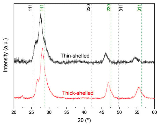
Figure 3.
X-ray diffraction (XRD) patterns of thick- (bottom) and thin-shelled (top) QDs.
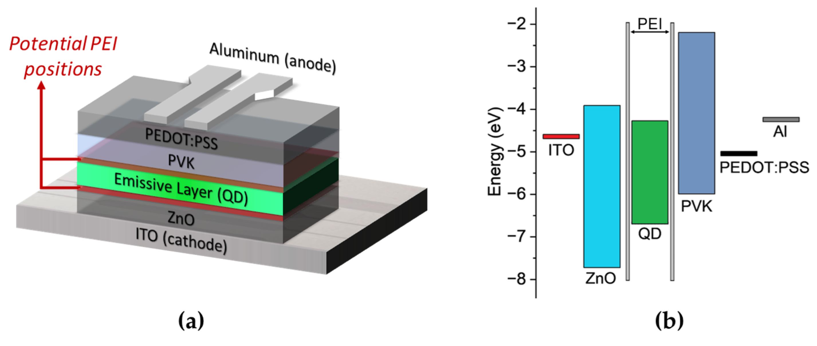
After growing QDs possessing two different shell thicknesses, we were ready to prepare their inverted LEDs. In our device architecture, as shown in Figure 4, we employed PEDOT:PSS as the hole injection layer, knowing that it improves the electrical parameters of optoelectronic devices [40]. For the rest of the device, we used QDs as the active layer, PVK and ZnO nanoparticles as the hole transport and electron injection layers, and indium–tin oxide and aluminum act as the cathode and anode. The HOMO levels of PVK and PEDOT:PSS are ∼6.0 eV [41] and ∼5.0 eV [42], respectively. The energy levels of ZnO, QDs, and PEI given in Figure 2b are sourced from previous studies [17,43,44]. To understand the effect of an amine-containing polymeric film on the device performance, we studied four different device architectures. Variations and their notations are as follows: (i) without PEI PEI (x-PEI), (ii) between ZnO and QD layer (e-PEI), (iii) between QD and PVK layer (h-PEI), and (iv) both sides of the QD layer (eh-PEI). All PEI layers in this set were formed by using 0.05 wt% ethoxyethanol solutions.

Figure 4.
Schematic illustration of (a) inverted QLED architecture and (b) energy band diagram.
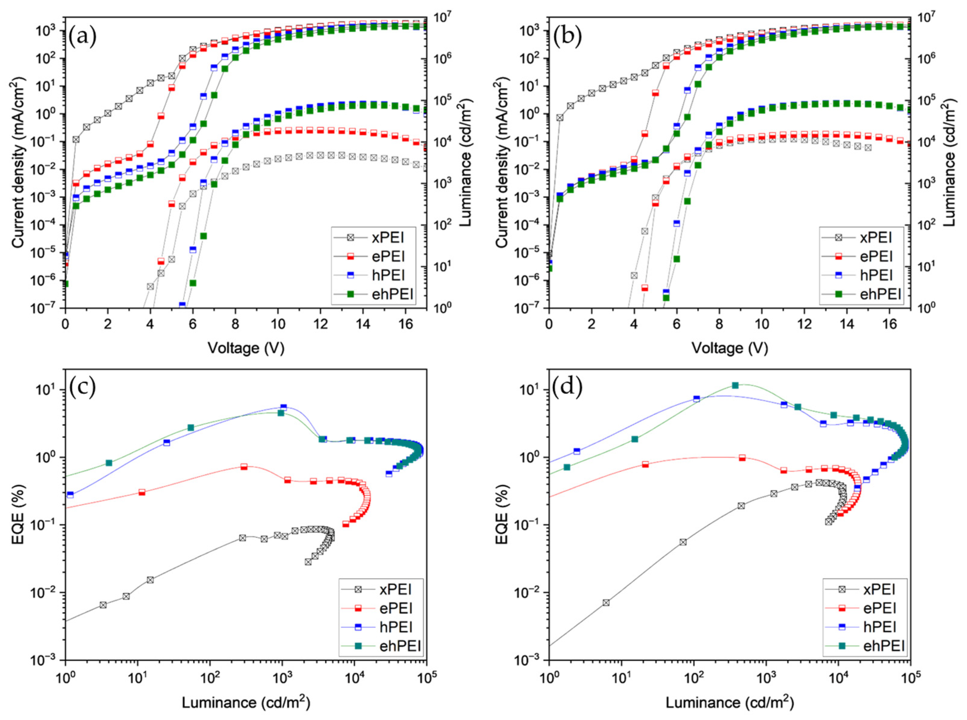
The energy transfer of an exciton to an adjacent QD is likely to result in a significant reduction in photoluminescence quantum yield (PLQY) due to annihilation of excitons by the possible trap sites. This phenomenon is more pronounced in closely packed solid films, similar to the ones used in the QLED structure. One approach to mitigate this issue, as demonstrated in this study, is to increase the shell thickness, thereby increasing the interspace between nanocrystals and suppressing QD charging and energy transfer [45]. Luminance–current density–voltage characteristics of the thick- and thin-shelled QLEDs with varying PEI layer positions are presented in Figure 5a,b. The maximum luminance values are 4777 cd/m2 and 11,780 cd/m2 for x-PEI, 15,065 cd/m2 and 18,747 cd/m2 for e-PEI, 81,322 cd/m2 and 84,627 cd/m2 for h-PEI, and 76,372 cd/m2 and 83,447 cd/m2 for eh-PEI with thin- and thick-shelled QDs, respectively. Peak luminance can be attributed to the charge balance optimization for the active layer. Other layers being equal, the effect of thicker shell is evident, with a clear improvement in both peak EQE and luminance values. Figure 5c,d demonstrate that the incorporation of PEI into the device architecture leads to a substantial enhancement in peak external quantum efficiency (EQE) performance. The highest EQE of 11.5% was achieved in the eh-PEI structure, where the thick-shelled QD active layer is sandwiched between two PEI layers. The second highest EQE of 7.3% was attained in the h-PEI device structure with the same QD type.
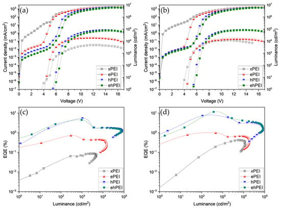
Figure 5.
Electroluminescence characteristics of x-PEI, e-PEI, h-PEI, and eh-PEI devices with (a,c) thin-shelled and (b,d) thick-shelled QD active layers.
The incorporation of the PEI layers in the device structure leads to an increase in the required voltage to achieve the threshold for carrier injection. This increase in driving voltage is directly proportional to the thickness of the PEI layers. However, devices with double PEI layers exhibit higher efficiency compared to control devices without PEI, suggesting that the inclusion of PEI layers provides certain advantages that outweigh the increased driving voltage.
For both thin- and thick-shelled QLED devices, the highest EQE values were achieved when the active layer was sandwiched between two PEI layers (eh-PEI configuration). Although the peak luminance values of eh-PEI devices were comparable to those of devices with a single PEI layer positioned between the QD and PVK layers (h-PEI configuration), the eh-PEI devices exhibited a ~20% and ~60% improvement in peak EQE performance for thin- and thick-shelled QDs, respectively. The summary of the characterization results is given in Table 1.

Table 1.
Electroluminescence characteristics of x-PEI, e-PEI, h-PEI, and eh-PEI devices with thin- and thick-shelled QDs.
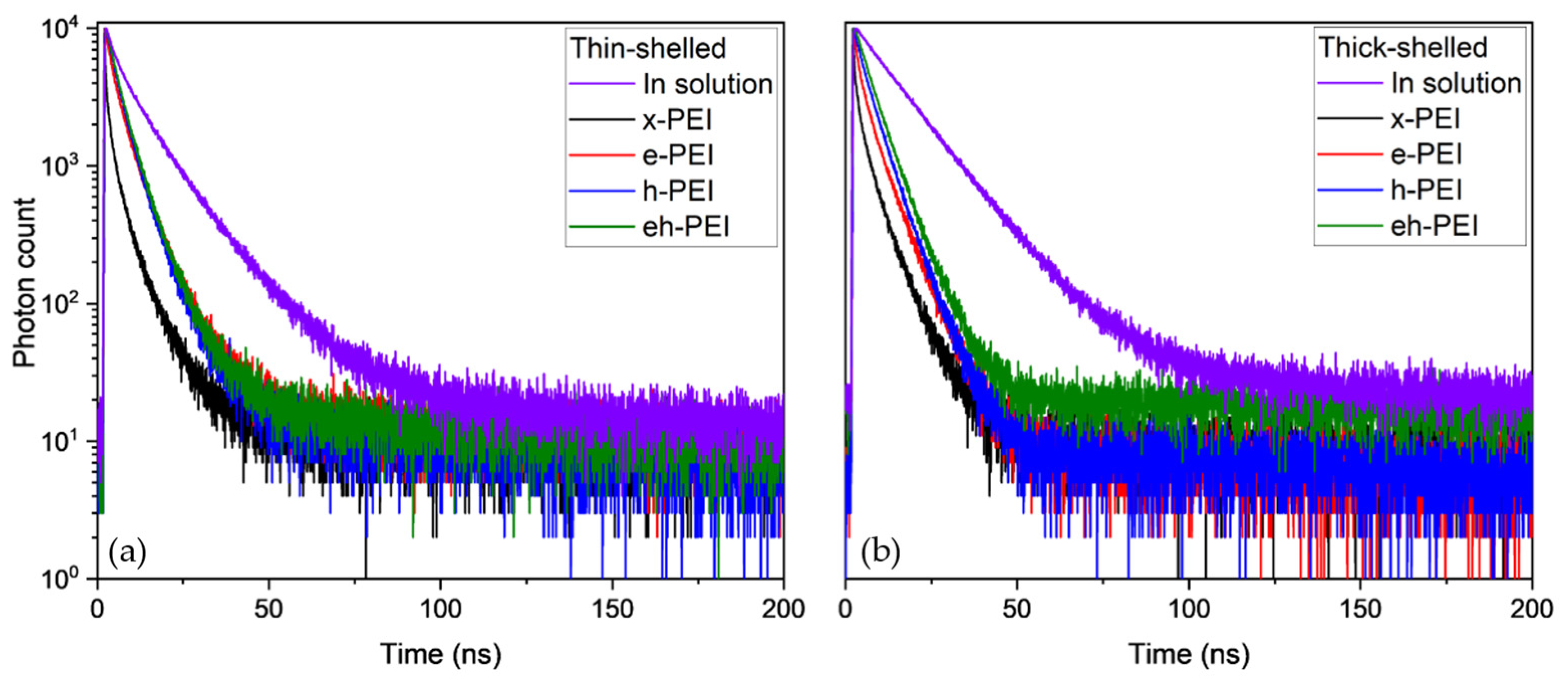
Time-resolved photoluminescence (TRPL) measurements were performed to investigate the interaction between quantum dots (QDs) and adjacent layers by exciting the samples at a wavelength of 371 nm. Closely packed films in four different device architectures were compared to QDs in solution. As shown in Figure 6 and Table 2, the incorporation of PEI in various positions resulted in longer average lifetimes for both thin- and thick-shelled QDs. The longer average lifetime of thick-shelled QDs in solution (13.5 ns) compared to their thin-shelled counterparts (8.5 ns) supports the aforementioned claims regarding the role of thicker shells and in agreement with the findings in the literature that increased interparticle distance is translated into a longer average lifetime [46].

Figure 6.
Time-resolved photoluminescence of x-PEI, e-PEI, h-PEI, and eh-PEI devices and in-solution sample with (a) thin-shelled and (b) thick-shelled QDs.

Table 2.
TRPL fitting parameters of thin- and thick-shelled QDs in solution and in the four different device structures.
The average lifetimes were 1.40 ns and 1.93 ns when the thin-shelled and thick-shelled QDs were positioned between ZnO and PVK layers, respectively. Respective average lifetimes became 3.98 ns and 3.68 ns when a PEI layer was coated between the ZnO and QD layers, 4.23 ns and 4.90 ns when the PEI layer was placed between the QD and PVK layers, and 4.43 ns and 5.53 ns for devices in which the QDs were sandwiched between two PEI layers. Although a significant drop in the average lifetime is expected in the device structure due to the physical confinement of QDs in a closely packed thin film, the introduction of PEI into the device architecture improved the device performance. This suggests that the decrease in average lifetime is not solely caused by the reduced interparticle distance but also by the exciton quenching induced by adjacent layers. The PEI layer appears to play a role in passivating QDs and suppressing this phenomenon for both QD types.
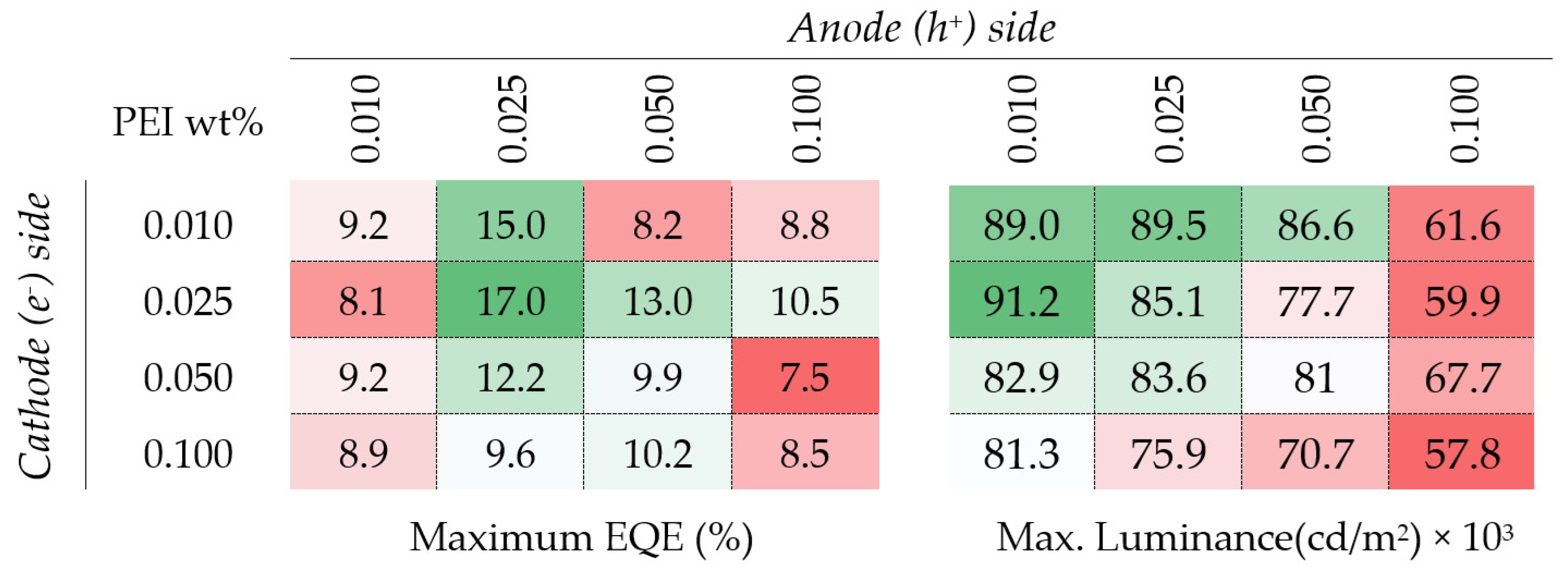
To further investigate the effect of interfacial dipole intensity on device performance, a set of devices was fabricated using thick-shelled QDs in an eh-PEI configuration, which was the best performing architecture in a set with 0.05 wt% PEI concentration. In addition to the passivation effect of PEI, it is well established that the presence of protonated amines in PEI induces electrostatic dipoles at the interface with adjacent semiconductors or metals [47]. PEI concentrations of 0.010, 0.025, 0.050, and 0.100 wt% were employed in each of the two PEI layers, resulting in a total of 16 different device configurations.
A heatmap shown in Figure 7 was generated with the maximum EQE and maximum luminance values, where columns represent the PEI concentration between QD and PVK, while rows show the PEI concentration between ZnO and QD. The incorporation of PEI into the device structure significantly enhances performance, irrespective of the concentration utilized. However, optimal performance is achieved when a PEI concentration of 0.025 wt% is employed on both the anode and cathode sides of the active layer. On the anode side, this concentration effectively reduces the hole-injection barrier between the hole transport layer and QD layer, promoting charge balance. PEI forms a dipole layer that lowers the vacuum level, while its amine group acts as an electron donor, passivating electron traps and minimizing nonradiative exciton loss. On the cathode side, the optimal PEI concentration is a result of the combined effect of PEI’s intrinsic insulating properties and its ability to lower the work function. The insulating nature of PEI has a more pronounced impact than the enhanced electron injection resulting from the reduced work function. Consequently, higher PEI concentrations on either side of the active layer begin to impede efficient charge injection into the QD layer, leading to lower peak EQE levels. Furthermore, the maximum luminance values exhibit a negative correlation with the PEI concentration on both the anode and cathode sides. Increasing the PEI concentration on either the hole transport side or the cathode side adversely affects the maximum luminance performance. This phenomenon can be attributed to the reduced current density caused by the insulating properties of PEI.
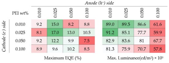
Figure 7.
Heatmap of maximum EQE and luminance values of the devices with varying PEI concentration, where red indicates lower and green indicates higher values.
4. Conclusions
In conclusion, this study demonstrates the significant impact of QD shell thickness and PEI interlayer optimization on the performance of inverted QLED structure. By employing a one-pot synthesis method, we successfully fabricated thick-shelled QDs with a diameter of 10.3 nm, which exhibited superior optical properties compared to their thin-shelled counterparts with an average particle size of 8.0 nm. The incorporation of PEI layers on both sides of the emissive layer proved to be a highly effective approach to enhancing device efficiency and luminance. Notably, the dual-sided PEI configuration with an optimized concentration of 0.025 wt% led to a maximum EQE of 17% and a peak luminance of 91,174 cd/m2. These findings highlight the importance of QD shell engineering and interfacial modification in optimizing the performance of inverted QLEDs. As display technology advances, the strategies presented here, such as dual-sided PEI interlayers with optimized concentration, could play a role in the development of efficient, bright, and color-pure quantum dot displays.
Author Contributions
Conceptualization, A.F.Y., T.E. and E.M.; methodology, A.F.Y., A.B. and S.K.O.; formal analysis, A.F.Y., T.E., E.M., E.U., A.U., R.K. and R.B.S.; investigation, A.F.Y., E.M. and T.E.; data curation, A.F.Y.; writing—original draft preparation, A.F.Y., T.E. and E.M.; writing—review and editing, A.F.Y., T.E. and E.M.; supervision, E.M. and T.E.; project administration, E.M.; funding acquisition, E.M. All authors have read and agreed to the published version of the manuscript.
Funding
Authors acknowledge the funding from ASELSAN and TUBITAK project no. 20AG026.
Institutional Review Board Statement
Not applicable.
Informed Consent Statement
Not applicable.
Data Availability Statement
The raw data supporting the conclusions of this article will be made available by the authors on request.
Acknowledgments
TE and EM acknowledge Science Academy for the BAGEP Award and Turkish Academy of Sciences (TÜBA) for the GEBİP Award.
Conflicts of Interest
The authors declare no conflicts of interest.
References
- Reed, M.A.; Bate, R.T.; Bradshaw, K.; Duncan, W.M.; Frensley, W.R.; Lee, J.W.; Shih, H.D. Spatial Quantization in GaAs–AlGaAs Multiple Quantum Dots. J. Vac. Sci. Technol. B Microelectron. Process. Phenom. 1986, 4, 358–360. [Google Scholar] [CrossRef]
- Mo, J. Recent Advances of Colloidal Quantum Dots in a Physical Perspective. J. Phys. Conf. Ser. 2023, 2634, 012017. [Google Scholar] [CrossRef]
- Peng, L.; Geng, J.; Ai, L.; Zhang, Y.; Xie, R.; Yang, W. Room Temperature Synthesis of Ultra-Small, near-Unity Single-Sized Lead Halide Perovskite Quantum Dots with Wide Color Emission Tunability, High Color Purity and High Brightness. Nanotechnology 2016, 27, 335604. [Google Scholar] [CrossRef] [PubMed]
- Li, X.; Wu, Y.; Steel, D.; Gammon, D.; Stievater, T.H.; Katzer, D.S.; Park, D.; Piermarocchi, C.; Sham, L.J. An All-Optical Quantum Gate in a Semiconductor Quantum Dot. Science 2003, 301, 809–811. [Google Scholar] [CrossRef] [PubMed]
- Frecker, T.; Bailey, D.; Arzeta-Ferrer, X.; McBride, J.; Rosenthal, S.J. Review—Quantum Dots and Their Application in Lighting, Displays, and Biology. ECS J. Solid State Sci. Technol. 2016, 5, R3019–R3031. [Google Scholar] [CrossRef]
- Han, C.; Qian, R.; Xiang, C.; Qian, L. Materials and Device Engineering to Achieve High-Performance Quantum Dots Light Emitting Diodes for Display Applications. Chin. Phys. B 2023, 32, 128506. [Google Scholar] [CrossRef]
- Al-Hetty, H.R.A.K.; Jalil, A.T.; Al-Tamimi, J.H.Z.; Shakier, H.G.; Kandeel, M.; Saleh, M.M.; Naderifar, M. Engineering and Surface Modification of Carbon Quantum Dots for Cancer Bioimaging. Inorg. Chem. Commun. 2023, 149, 110433. [Google Scholar] [CrossRef]
- Wahab, R.; Khan, F.; Alam, M.; Ahmad, J.; Al-Khedhairy, A.A. Aluminum Oxide Quantum Dots (Al2O3): An Immediate Sensing Aptitude for the Detection of Urea. Inorg. Chem. Commun. 2023, 147, 110238. [Google Scholar] [CrossRef]
- Wen, Z.; Zhou, Z.; Liu, H.; Wang, Z.; Li, X.; Fang, F.; Wang, K.; Teo, K.L.; Sun, X.W. Color Revolution: Toward Ultra-Wide Color Gamut Displays. J. Phys. D Appl. Phys. 2021, 54, 213002. [Google Scholar] [CrossRef]
- Yin, Y.; Hu, Z.; Ali, M.U.; Duan, M.; Gao, L.; Liu, M.; Peng, W.; Geng, J.; Pan, S.; Wu, Y.; et al. Full-Color Micro-LED Display with CsPbBr3 Perovskite and CdSe Quantum Dots as Color Conversion Layers. Adv Mater. Technol. 2020, 5, 2000251. [Google Scholar] [CrossRef]
- Triana, M.A.; Restrepo, A.A.; Lanzafame, R.J.; Palomaki, P.; Dong, Y. Quantum Dot Light-Emitting Diodes as Light Sources in Photomedicine: Photodynamic Therapy and Photobiomodulation. J. Phys. Mater. 2020, 3, 032002. [Google Scholar] [CrossRef]
- Zhang, D.; Huang, T.; Duan, L. Emerging Self-Emissive Technologies for Flexible Displays. Adv. Mater. 2020, 32, 1902391. [Google Scholar] [CrossRef]
- Chen, L.; Qin, Z.; Chen, S. Ultrahigh Resolution Pixelated Top-Emitting Quantum-Dot Light-Emitting Diodes Enabled by Color-Converting Cavities. Small Methods 2022, 6, 2101090. [Google Scholar] [CrossRef] [PubMed]
- Shim, G.W.; Hong, W.; Cha, J.; Park, J.H.; Lee, K.J.; Choi, S. TFT Channel Materials for Display Applications: From Amorphous Silicon to Transition Metal Dichalcogenides. Adv. Mater. 2020, 32, 1907166. [Google Scholar] [CrossRef] [PubMed]
- Kwak, J.; Bae, W.K.; Lee, D.; Park, I.; Lim, J.; Park, M.; Cho, H.; Woo, H.; Yoon, D.Y.; Char, K.; et al. Bright and Efficient Full-Color Colloidal Quantum Dot Light-Emitting Diodes Using an Inverted Device Structure. Nano Lett. 2012, 12, 2362–2366. [Google Scholar] [CrossRef] [PubMed]
- Zhong, Z.; Zou, J.; Jiang, C.; Lan, L.; Song, C.; He, Z.; Mu, L.; Wang, L.; Wang, J.; Peng, J.; et al. Improved Color Purity and Efficiency of Blue Quantum Dot Light-Emitting Diodes. Org. Electron. 2018, 58, 245–249. [Google Scholar] [CrossRef]
- Ding, K.; Chen, H.; Fan, L.; Wang, B.; Huang, Z.; Zhuang, S.; Hu, B.; Wang, L. Polyethylenimine Insulativity-Dominant Charge-Injection Balance for Highly Efficient Inverted Quantum Dot Light-Emitting Diodes. ACS Appl. Mater. Interfaces 2017, 9, 20231–20238. [Google Scholar] [CrossRef] [PubMed]
- Shi, Y.-L.; Liang, F.; Hu, Y.; Zhuo, M.-P.; Wang, X.-D.; Liao, L.-S. High Performance Blue Quantum Dot Light-Emitting Diodes Employing Polyethylenimine Ethoxylated as the Interfacial Modifier. Nanoscale 2017, 9, 14792–14797. [Google Scholar] [CrossRef] [PubMed]
- Yuan, Y.; Xue, X.; Wang, T.; Chi, X.; Wang, R.; Ji, W. Polyethylenimine Modified Sol-Gel ZnO Electron-Transporting Layers for Quantum-Dot Light-Emitting Diodes. Org. Electron. 2022, 100, 106393. [Google Scholar] [CrossRef]
- Cun, Y.; Mai, C.; Luo, Y.; Mu, L.; Li, J.; Cao, L.; Yu, D.; Li, M.; Zhang, B.; Li, H.; et al. All-Solution Processed High Performance Inverted Quantum Dot Light Emitting Diodes. J. Mater. Chem. C 2020, 8, 4264–4270. [Google Scholar] [CrossRef]
- Courtright, B.A.E.; Jenekhe, S.A. Polyethylenimine Interfacial Layers in Inverted Organic Photovoltaic Devices: Effects of Ethoxylation and Molecular Weight on Efficiency and Temporal Stability. ACS Appl. Mater. Interfaces 2015, 7, 26167–26175. [Google Scholar] [CrossRef]
- Lee, T.; Kim, B.J.; Lee, H.; Hahm, D.; Bae, W.K.; Lim, J.; Kwak, J. Bright and Stable Quantum Dot Light-Emitting Diodes. Adv. Mater. 2022, 34, 2106276. [Google Scholar] [CrossRef] [PubMed]
- Lim, J.; Park, Y.-S.; Wu, K.; Yun, H.J.; Klimov, V.I. Droop-Free Colloidal Quantum Dot Light-Emitting Diodes. Nano Lett. 2018, 18, 6645–6653. [Google Scholar] [CrossRef] [PubMed]
- Lee, K.-H.; Lee, J.-H.; Song, W.-S.; Ko, H.; Lee, C.; Lee, J.-H.; Yang, H. Highly Efficient, Color-Pure, Color-Stable Blue Quantum Dot Light-Emitting Devices. ACS Nano 2013, 7, 7295–7302. [Google Scholar] [CrossRef] [PubMed]
- Park, Y.-S.; Bae, W.K.; Padilha, L.A.; Pietryga, J.M.; Klimov, V.I. Effect of the Core/Shell Interface on Auger Recombination Evaluated by Single-Quantum-Dot Spectroscopy. Nano Lett. 2014, 14, 396–402. [Google Scholar] [CrossRef] [PubMed]
- Yang, Y.; Zheng, Y.; Cao, W.; Titov, A.; Hyvonen, J.; Manders, J.R.; Xue, J.; Holloway, P.H.; Qian, L. High-Efficiency Light-Emitting Devices Based on Quantum Dots with Tailored Nanostructures. Nat. Photonics 2015, 9, 259–266. [Google Scholar] [CrossRef]
- Jun, S.; Jang, E. Bright and Stable Alloy Core/Multishell Quantum Dots. Angew. Chem. Int. Ed. 2013, 52, 679–682. [Google Scholar] [CrossRef] [PubMed]
- Shen, H.; Wang, S.; Wang, H.; Niu, J.; Qian, L.; Yang, Y.; Titov, A.; Hyvonen, J.; Zheng, Y.; Li, L.S. Highly Efficient Blue–Green Quantum Dot Light-Emitting Diodes Using Stable Low-Cadmium Quaternary-Alloy ZnCdSSe/ZnS Core/Shell Nanocrystals. ACS Appl. Mater. Interfaces 2013, 5, 4260–4265. [Google Scholar] [CrossRef]
- Bae, W.K.; Char, K.; Hur, H.; Lee, S. Single-Step Synthesis of Quantum Dots with Chemical Composition Gradients. Chem. Mater. 2008, 20, 531–539. [Google Scholar] [CrossRef]
- Lee, K.-H.; Lee, J.-H.; Kang, H.-D.; Park, B.; Kwon, Y.; Ko, H.; Lee, C.; Lee, J.; Yang, H. Over 40 Cd/A Efficient Green Quantum Dot Electroluminescent Device Comprising Uniquely Large-Sized Quantum Dots. ACS Nano 2014, 8, 4893–4901. [Google Scholar] [CrossRef]
- Vela, J.; Htoon, H.; Chen, Y.; Park, Y.; Ghosh, Y.; Goodwin, P.M.; Werner, J.H.; Wells, N.P.; Casson, J.L.; Hollingsworth, J.A. Effect of Shell Thickness and Composition on Blinking Suppression and the Blinking Mechanism in ‘Giant’ CdSe/CdS Nanocrystal Quantum Dots. J. Biophotonics 2010, 3, 706–717. [Google Scholar] [CrossRef] [PubMed]
- Omogo, B.; Gao, F.; Bajwa, P.; Kaneko, M.; Heyes, C.D. Reducing Blinking in Small Core–Multishell Quantum Dots by Carefully Balancing Confinement Potential and Induced Lattice Strain: The “Goldilocks” Effect. ACS Nano 2016, 10, 4072–4082. [Google Scholar] [CrossRef] [PubMed]
- Yang, H.; Zhang, L.; Tang, Y.; Xiang, W.; Wang, X.; Xiao, M.; Cui, Y.; Zhang, J. Enhanced Multiexciton Emission Property in Gradient Alloy Core/Shell CdZnSeS/ZnS Quantum Dots: Balance between Surface Passivation and Strain-Induced Lattice Defect. J. Phys. Chem. C 2021, 125, 10759–10767. [Google Scholar] [CrossRef]
- Roy, D.; De, C.K.; Ghosh, S.; Mukherjee, S.; Mandal, S.; Mandal, P.K. Ultrafast Dynamics and Ultrasensitive Single Particle Spectroscopy of Optically Robust Core/Alloy Shell Semiconductor Quantum Dots. Phys. Chem. Chem. Phys. 2022, 24, 8578–8590. [Google Scholar] [CrossRef] [PubMed]
- Fu, Y.; Kim, D.; Jiang, W.; Yin, W.; Ahn, T.K.; Chae, H. Excellent Stability of Thicker Shell CdSe@ZnS/ZnS Quantum Dots. RSC Adv. 2017, 7, 40866–40872. [Google Scholar] [CrossRef]
- Wang, O.; Wang, L.; Li, Z.; Xu, Q.; Lin, Q.; Wang, H.; Du, Z.; Shen, H.; Li, L.S. High-Efficiency, Deep Blue ZnCdS/CdxZn1−xS/ZnS Quantum-Dot-Light-Emitting Devices with an EQE Exceeding 18%. Nanoscale 2018, 10, 5650–5657. [Google Scholar] [CrossRef] [PubMed]
- Linkov, P.; Samokhvalov, P.; Vokhmintsev, K.; Zvaigzne, M.; Krivenkov, V.A.; Nabiev, I. Optical Properties of Quantum Dots with a Core–Multishell Structure. JETP Lett. 2019, 109, 112–115. [Google Scholar] [CrossRef]
- Gray, V.; Xia, P.; Huang, Z.; Moses, E.; Fast, A.; Fishman, D.A.; Vullev, V.I.; Abrahamsson, M.; Moth-Poulsen, K.; Lee Tang, M. CdS/ZnS Core–Shell Nanocrystal Photosensitizers for Visible to UV Upconversion. Chem. Sci. 2017, 8, 5488–5496. [Google Scholar] [CrossRef] [PubMed]
- Kurochkin, N.S.; Vashchenko, A.A.; Vitukhnovsky, A.G.; Tananaev, P.N. Effect of the Length of Ligands Passivating Quantum Dots on the Electrooptical Characteristics of Organic Light-Emitting Diodes. Semiconductors 2015, 49, 953–958. [Google Scholar] [CrossRef]
- Anatolyevich, E.M.; Mikhailov, I.I.; Tarasov, S.A.; Lamkin, I.A.; Tadtaev, P.O.; Degterev, A.E. Creation and Investigation of OLED-Structures with Inclusion of Colloidal Quantum Dots. J. Phys. Conf. Ser. 2018, 1038, 012103. [Google Scholar] [CrossRef]
- Shi, Y.-L.; Liang, F.; Hu, Y.; Wang, X.-D.; Wang, Z.-K.; Liao, L.-S. High-Efficiency Quantum Dot Light-Emitting Diodes Employing Lithium Salt Doped Poly(9-Vinlycarbazole) as a Hole-Transporting Layer. J. Mater. Chem. C 2017, 5, 5372–5377. [Google Scholar] [CrossRef]
- Xu, C.; Yang, S.; Tian, L.; Guo, T.; Ding, G.; Zhao, J.; Sun, J.; Lu, J.; Wang, Z. Fabrication of Centimeter-Scale Light-Emitting Diode with Improved Performance Based on Graphene Quantum Dots. Appl. Phys. Express 2017, 10, 032102. [Google Scholar] [CrossRef]
- Kim, D.; Fu, Y.; Kim, S.; Lee, W.; Lee, K.-H.; Chung, H.K.; Lee, H.-J.; Yang, H.; Chae, H. Polyethylenimine Ethoxylated-Mediated All-Solution-Processed High-Performance Flexible Inverted Quantum Dot-Light-Emitting Device. ACS Nano 2017, 11, 1982–1990. [Google Scholar] [CrossRef] [PubMed]
- Davidson-Hall, T.; Aziz, H. The Role of Polyethylenimine in Enhancing the Efficiency of Quantum Dot Light-Emitting Devices. Nanoscale 2018, 10, 2623–2631. [Google Scholar] [CrossRef] [PubMed]
- Lim, J.; Jeong, B.G.; Park, M.; Kim, J.K.; Pietryga, J.M.; Park, Y.; Klimov, V.I.; Lee, C.; Lee, D.C.; Bae, W.K. Influence of Shell Thickness on the Performance of Light-Emitting Devices Based on CdSe/Zn1-XCdXS Core/Shell Heterostructured Quantum Dots. Adv. Mater. 2014, 26, 8034–8040. [Google Scholar] [CrossRef] [PubMed]
- Kurochkin, N.S.; Katsaba, A.V.; Ambrozevich, S.A.; Vitukhnovsky, A.G.; Vashchenko, A.A.; Tananaev, P.N. Energy Transfer from TPD to CdSe/CdS/ZnS Colloidal Nanocrystals. Semiconductors 2017, 51, 628–631. [Google Scholar] [CrossRef]
- Kim, Y.; Han, T.; Cho, H.; Min, S.; Lee, C.; Lee, T. Polyethylene Imine as an Ideal Interlayer for Highly Efficient Inverted Polymer Light-Emitting Diodes. Adv. Funct. Mater. 2014, 24, 3808–3814. [Google Scholar] [CrossRef]
Disclaimer/Publisher’s Note: The statements, opinions and data contained in all publications are solely those of the individual author(s) and contributor(s) and not of MDPI and/or the editor(s). MDPI and/or the editor(s) disclaim responsibility for any injury to people or property resulting from any ideas, methods, instructions or products referred to in the content. |
© 2024 by the authors. Licensee MDPI, Basel, Switzerland. This article is an open access article distributed under the terms and conditions of the Creative Commons Attribution (CC BY) license (https://creativecommons.org/licenses/by/4.0/).

