Article

Design and Fabrication of Metasurfaces-Based Polarizing Beam Splitter with Tailored Deflection Angles for 940-nm Wavelength

Graduate Institute of Photonics and Optoelectronics, National Taiwan University, No. 1, Sec. 4, Roosevelt Rd., Taipei 10617, Taiwan
*
Author to whom correspondence should be addressed.
Photonics 2024, 11(7), 655; https://doi.org/10.3390/photonics11070655
Submission received: 29 April 2024 / Revised: 21 June 2024 / Accepted: 9 July 2024 / Published: 11 July 2024
(This article belongs to the Special Issue Polarization Optics)

Abstract

:
Polarizing beam splitters (PBSs) are fundamental components of optical systems and are crucial for sensing, communication, and imaging tasks. Traditional PBS devices, assembled using right-angle prisms with dielectric coatings, face challenges such as bulkiness and limited versatility in deflection directions. To address these limitations, we meticulously make metasurfaces for enhanced PBS performance. Metasurfaces, composed of subwavelength structures, manipulate wavefronts, polarization, and light intensity. Using metasurfaces in the design of PBS devices, we can precisely tailor the structure to manipulate the deflection angles of light beams, ensuring that they align with the desired specifications. Our experimental results closely align with simulation outcomes, showcasing deflection angles of a 1.5 mm diameter metasurface near ±15 degrees for s- and p-polarizations in a wavelength of 940-nm.

1. Introduction

In optical applications, Polarizing Beam Splitters (PBS) play a crucial role and are commonly employed in sensing, data storage, communication, imaging, and signal processing tasks related to polarization direction [1,2,3]. Traditional PBS devices are typically assembled by having two right-angle prisms bonded with dielectric coatings applied on their hypotenuse sides. In communication systems, the PBS can efficiently split and switch polarization states by controlling the birefringence of the waveguides and utilizing the Mach–Zehnder interferometer configuration [4], or the PBS with asymmetric structure is also able to increase bandwidth in fiber for guiding terahertz waves [5]. Although the traditional PBS is able to precisely redirect light into two orthogonal directions, its bulky size poses challenges in practical applications. Over the years, various approaches have been explored to reduce the size of PBS devices. Techniques such as utilizing the single binary phase Fresnel lenses [6] or designing Compact Photonic-Crystal-Based PBS [7] have been proposed. Additionally, the constraint imposed by the two fixed deflection directions also limits the versatility of PBS applications.
In order to break through the limitation of the angle and size of PBS, Metasurface has become one of the solutions that have been extensively researched because of their nanoscale size and versatility [8,9,10]. Metasurface is able to manipulate wavefronts, polarization, and light intensity by modifying the geometric parameters of the sub-wavelength structures [11]. Consequently, a lot of applications of metasurface are developed, such as metalens, metasurface holography, and beam splitter [12,13].
In the past few years, many research studies of metasurface-based PBS have been undertaken [14,15,16,17,18,19]. Most metasurface designs are constructed with nanopillars which have significantly different sizes to reduce fabrication errors. We present a PBS based on an a-Si metasurface for the 940-nm wavelength. In order to obtain more precise simulation results and high efficiency, the metasurface is meticulously structured with several nanopillars having very small size variations. According to our previous work [20], the finite-difference time-domain (FDTD) software from Lumerical Inc. and a geometrical optics design software from OpticStudio (Zemax, LLC) are applied to design and simulate the metasurface. We are going to show the simulation of the metasurfaces with different deflection angles. Additionally, we demonstrate the 1.5 mm diameter metasurfaces experimental results with a deflection angle of ±15 degrees for the s-polarized and p-polarized normal incident light.

2. Methods

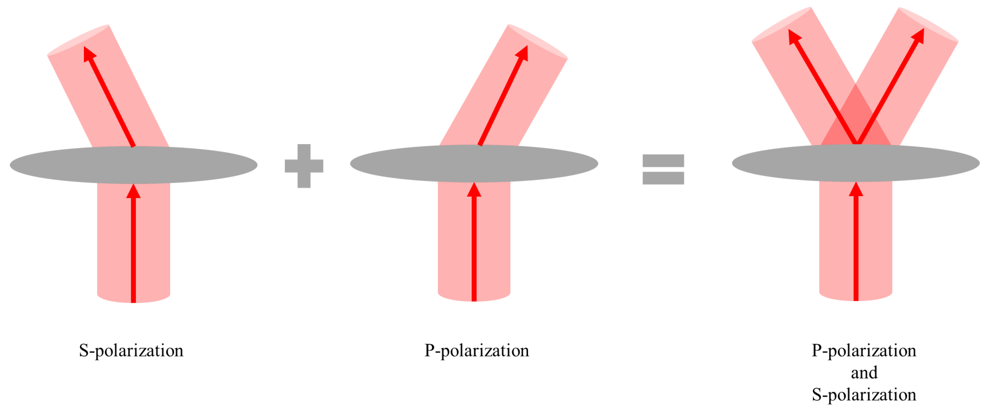
2.1. Ideal Phase Profile of the Metasurface

Metasurface-based designs are used for controlling the wavefront of light through the subwavelength structures on a surface. The nanopillars can be described by the Jones matrix of a conventional, linearly birefringent wave plate [21]
J = R ( θ ) e i ϕ x 0 0 e i ϕ y R ( θ ) ,
where ϕ x and ϕ y are the phase shift nanopillar imposes on light linearly polarized light along its fast and slow axes, which are rotated by an angle θ relative to the reference coordinate system (R is a 2 × 2 rotation matrix). In this work, θ is zero, so the Jones matrix becomes the following matrix
J = e i ϕ x 0 0 e i ϕ y .
After describing nanopillars with the Jones matrix, the ideal phase profile of the metasurface is able to be realized by the phase shift provided by nanopillars. According to the generalized Snell’s law [22], the ideal phase profile required to deflect a normally incident wave by θ is calculated by Equation (3):
ϕ ( x , y ) = 2 π λ x sin θ
where x, λ , and θ are coordinate, wavelength, and deflection angle. In order to realize the function of polarization beam splitting, namely, the c incident wave is deflected at two different angles θ x and θ y , the ideal phase profile needs to be constructed of two dimension phase distribution, ϕ x = 2 π λ x sin θ x and ϕ y = 2 π λ y sin θ y , for s- and p-polarizations.
In recent years, some researchers have used the optical software Optic Studio (Zemax, LLC) [23,24,25] in order to obtain the phase profile. The phase profile is defined as following Equation (4)
ϕ d e s i g n ( x , y ) = M i = 1 n a n ( ρ R ) 2 i
where M is the diffraction order, R is the normalised radius of the metasurface, ρ is the radius along the plane of the metasurface, and a n is the optimization coefficients minimize the focal spot size, which in our work is used to maintain the spot size of light through the metasurface because the metasurface-based PBS, in this case, does not need to have the focus ability.

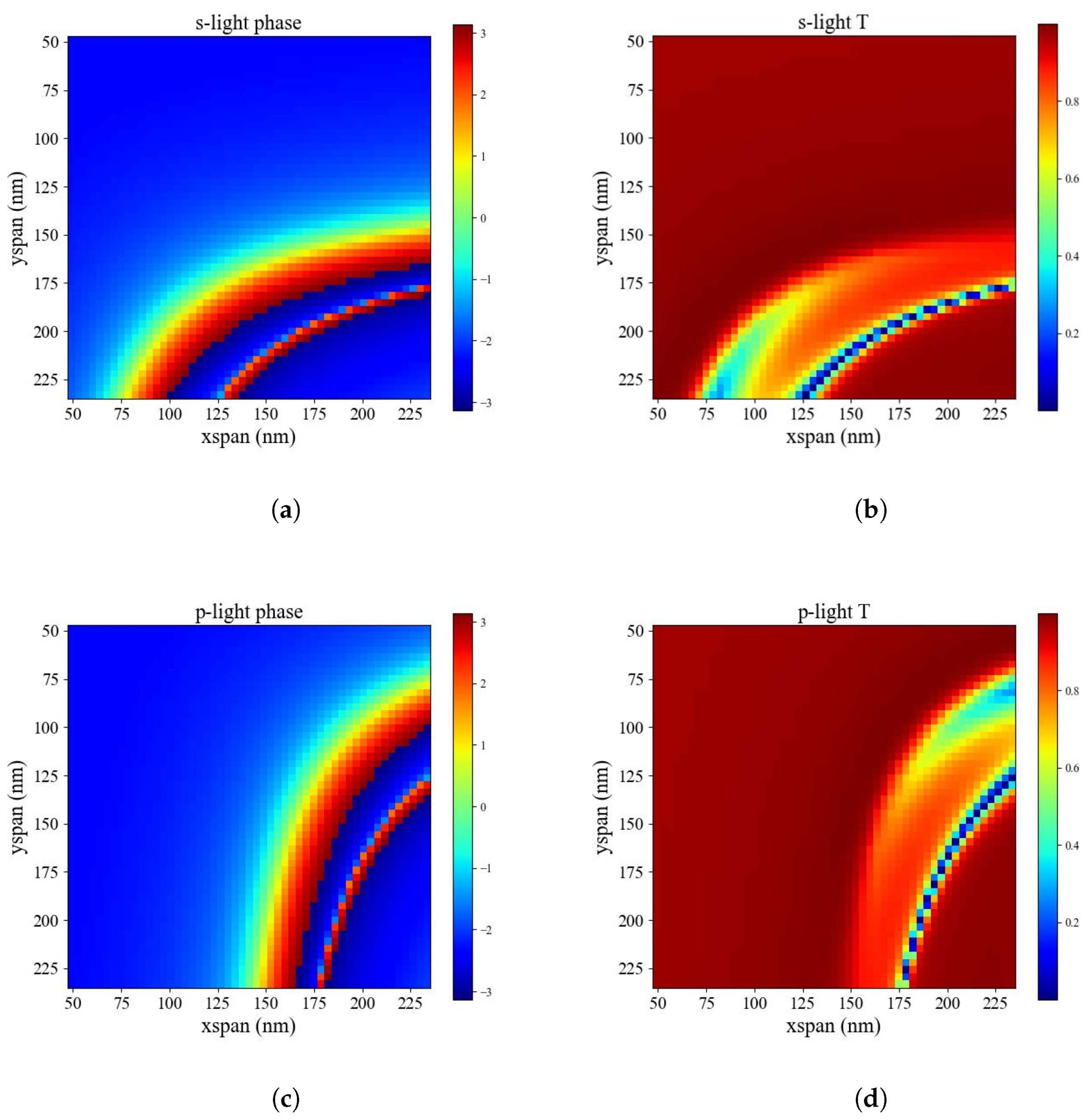
2.2. Design of Metasurface

To simulate the phase delay caused by nanopillars, we designed the 50-μm diameter metasurfaces with deflection angles the same as 1.5 mm diameter metasurface, which was the limitation of our computer resources. We used a-Si nanopillars to design the metasurface PBS for 940-nm wavelength and selected SiO2 as the material of the substrate. The scheme is shown in Figure 1; a normally incident s-polarized or p-polarized light would be deflected to different angles through the same metasurface when s-polarized and p-polarized light simultaneously passes through the metasurface, the light would be split in different angles according to polarization. The period of the unit cell in the metasurface was 450-nm, and its height was 570-nm; the unit cell is shown in Figure 2. The phase shift varies with the size of the nanopillars; therefore, in order to cover the entire 0 to 2 π phase, we scanned the length and width of the nanopillar in 50 points from 45-nm to 248-nm in each dimension, then built the database of phase shift changes as a function of length and width by using the commercial FDTD software from Lumerical. The phase shift imposed by nanopillars and transmission efficiency of the unit cell as a function of length (xspan) and width (ysapn) for s-polarization and p-polarization is shown in Figure 3. Nanopillars were selected with proper transmission efficiency. In order to fit the ideal phase profile on the metasurfaces as closely as possible, we expand the database to 100 × 100 nanopillars by interpolation method. After building the database, we constructed the metasurface with the nanopillars database according to the ideal phase profile calculated by Equation (4), We first fit the ideal phase profile for s-polarization and then fit the ideal phase profile for p-polarization without affecting the s-polarization part as much as possible, the phase mismatch between phase imposed by unit cell and ideal phase profile is quite small. If the deviation of the phase profile is too large, the light will not be deflected smoothly to the target angle, resulting in the generation of many additional diffraction orders.

3. Results

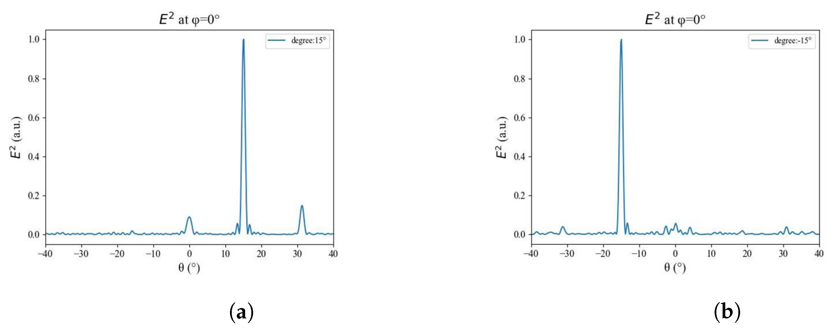
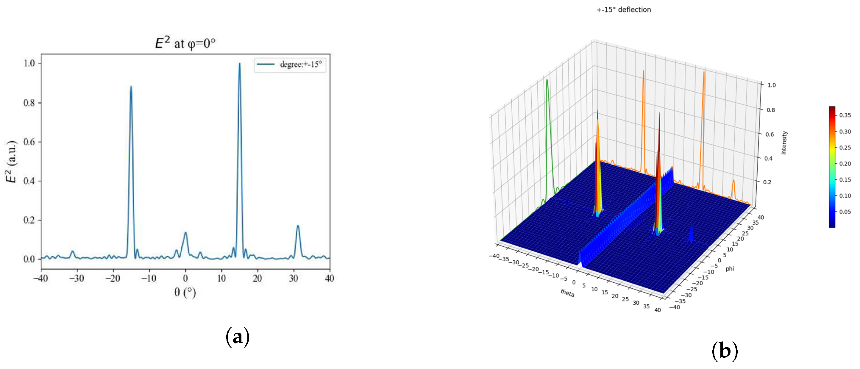
3.1. Simulation Results

The simulation results for the metasurface with deflection angles ±15 degrees are shown in Figure 4 using the FDTD method. Figure 4a,b present the normalized power as a function of angle for s-polarized and p-polarized incident light at a wavelength of 940-nm, respectively. As is clearly shown, power is almost concentrated at a deflection angle of +15 and −15 degrees, as expected; the exact deflection angles are 14.94 degrees and −15.12 degrees. The total transmission efficiencies are 81.5% and 78.6%, defined as the ratio of the power of light passing through the metasurface to light source power, and the deflection efficiencies, defined as the ratio of the detected optical power at a deflection position 100-mm from the metasurface to light source power, are 47.11% and 41.50% for deflection angles 14.94 degrees and −15.12 degrees, respectively. Figure 5 demonstrates the simulation result with incident light consisting of s- and p-polarizations; power distribution is almost the same as the combination of Figure 4a,b.
In addition to that, we also simulated different deflection angles from 5 to 30 degrees for s-polarization and −5 to −30 degrees for p-polarization. Figure 6 presents the total transmission efficiencies and deflection efficiencies for different deflection angles. According to Figure 6, the efficiency for positive deflection angles (s-polarization) is more stable than that for negative angles (p-polarization). This is because the phase shifts imposed by the nanopillars cannot perfectly satisfy the ideal phase profiles for both s- and p-polarizations simultaneously. Consequently, our designed metasurface-based PBS cannot fully deflect the incident light to the correct deflection angles. According to simulation results, this phenomenon becomes more severe as the deflection angle of the metasurface becomes larger. In this work, deflection angles ±30 degrees are the limitation for our design; if the deflection angle exceeds ±30 degrees, the total transmission efficiencies are too low for practical application.

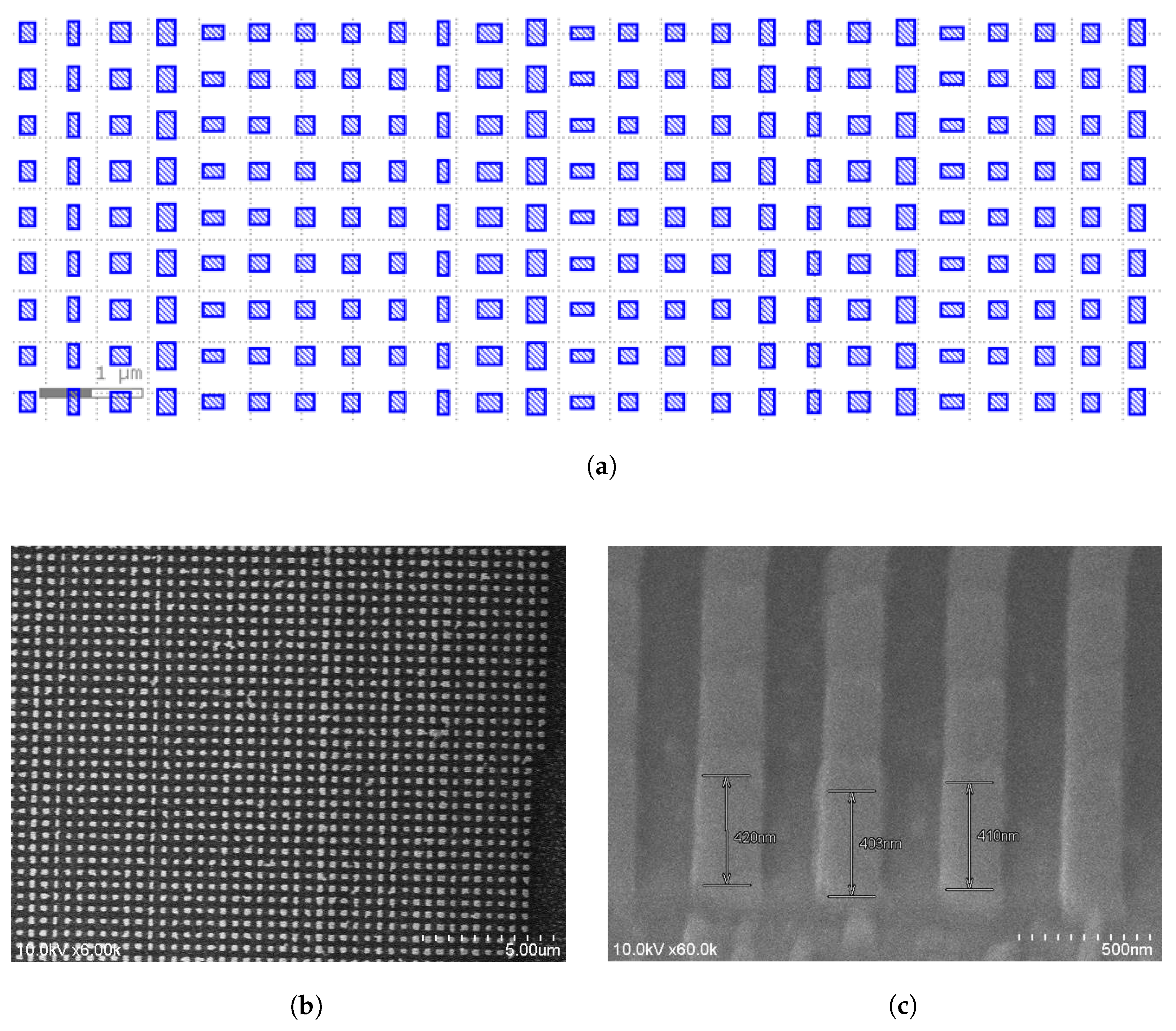
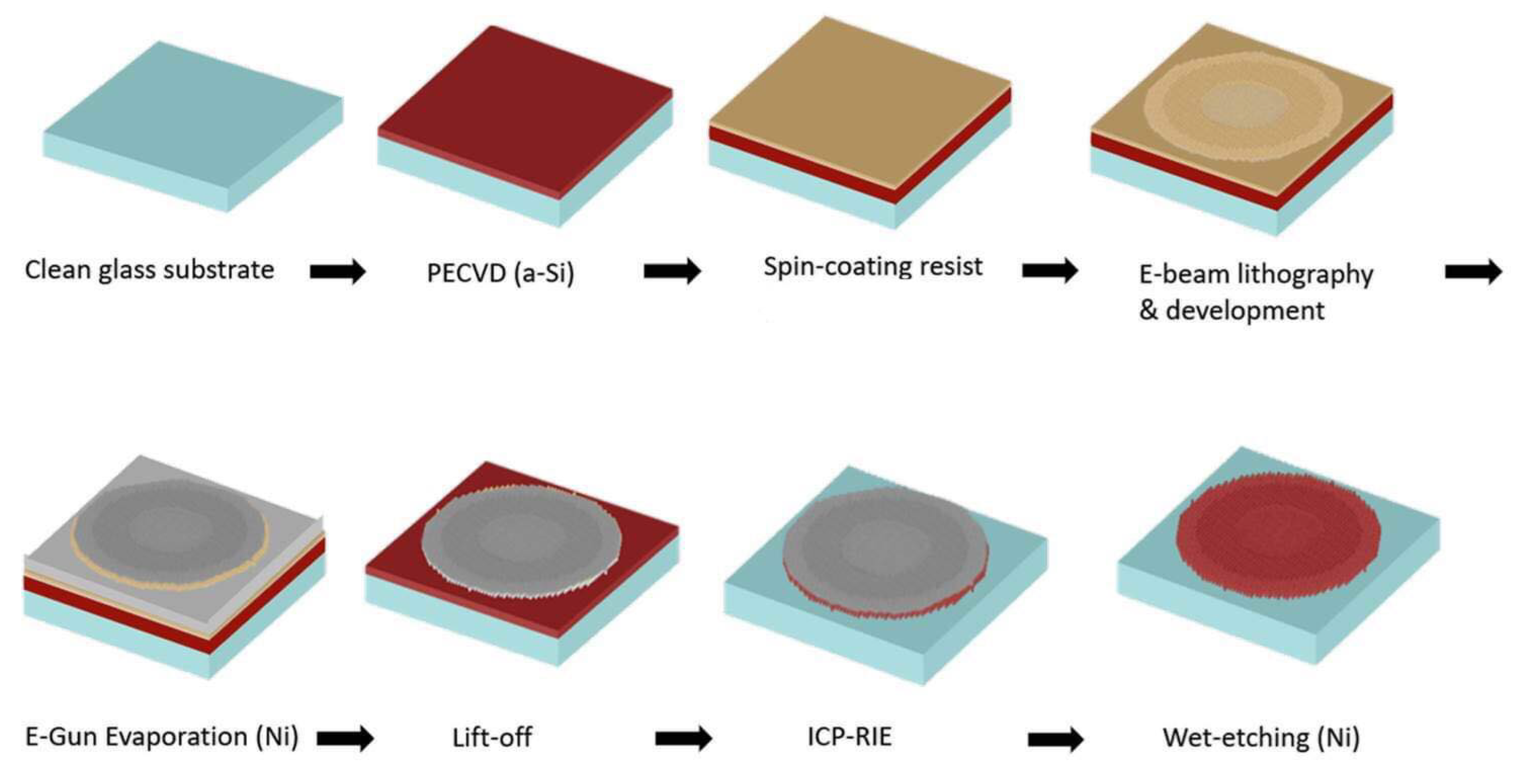
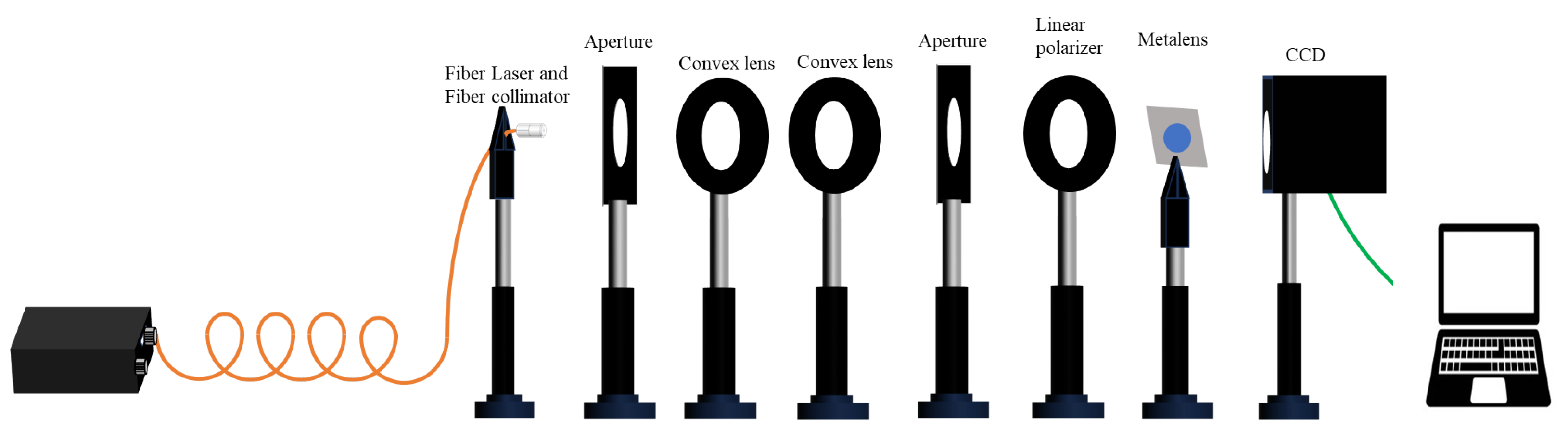
3.2. Experimental Results

Figure 7a is the GDSII file of diameter 1.5 mm metasurface-based PBS. The fabrication process is shown in Figure 8. First, the SiO2 substrate is cleaned in acetone and methanol. After cleaning, the substrate is placed in a UV-Ozone cleaner to remove any remaining organic residues. Second, a 600-nm thick silicon layer is deposited on the sapphire substrate using plasma-enhanced chemical vapor deposition (PECVD), serving as the primary layer for the metasurface. For the exposure process, the positive photoresist is spin-coated onto the silicon layer using a spin coater, and the substrate is soft-baked on a hotplate at 180 °C for 60 s. Subsequently, the metasurface pattern, consisting of nanopillar structures, is initially defined and developed using electron beam lithography (E-Beam lithography). After exposure, the samples are developed in pentyl acetate (N50 developer, ZEON Corporation) for 5 min and rinsed in DI water. The samples undergo a hard bake step at 130 °C for 60 s. Nickel (Ni) is deposited using electron beam evaporation (E-Gun) to serve as the hard mask. After depositing Ni, a lift-off process is performed. With the metasurface pattern successfully created on the substrate, an etching process is employed to obtain silicon nanopillars. We have adopted a continuous, multi-step ICP-RIE process by adjusting O2/SF6 gas flows. During the dry etching step, silicon is etched using Ni as the hard mask with a gas mixture of O2 and SF6. Finally, a wet etching process with H2SO4 and H2O2 for 180 s is conducted to remove the Ni metal. SEM images of the metasurface are shown in Figure 7b,c with a 45-degree top view, the height of nanopillars approximately equal to 581-nm.
The experimental setup for the measurement is shown in Figure 9. The fiber laser for 940-nm laser with 1.5 mm spot size was the light source collimated by fiber collimator, the aperture and convex lenses are used to limit the large light coming out of the collimator, the linear polarizer is used to generate s- and p-polarized light, the metasurface was placed behind of the linear polarizer, and the CCD was placed 100 mm away from the metasurface.
The experimentally measured normalized power distribution as a function of deflection angles is shown in Figure 10; we have utilized curve fitting to modify our actual experimental results. The measured deflection angles are 15.34 degrees and −15.75 degrees, corresponding to s- and p-polarizations, the deflection efficiencies are 41.54% and 36.92%, the power distribution of experimental results closely align with simulation result shown in Figure 5; in the other words, the actual power distribution can be observed through simulation with meticulous design. These results also demonstrate that the meticulous construction of metasurface-based PBS has the ability to deflect at different angles with good performance through our design method and fabrication process.
We list the comparison of our method and related works in Table 1. In addition to related work [18], other work has simulation and experimental verification. In this work, we demonstrate a cost-effective metasurface using a-Si material working at 940-nm. Since the 940-nm wavelength from sunlight is almost absorbed by water vapor in the atmosphere, sensor interference at the 940-nm wavelength is low; therefore, it is often used as a sensing light source, such as LiDARs and medical devices. Although the deflection angle is smaller than other related works, our metasurface offers 570-nm thickness and deflection efficiencies of over 35% for both s- and p-polarization at infrared wavelengths. In order to improve the problem of insufficient deflection angle and efficiency with using a-Si material, the nanopillars database needs to be expanded by scanning other specifications of unit cells; in addition, the matching method between the ideal phase profile and the phase profile imposed by the nanopillars also needs to be improved.

4. Conclusions

In this work, we have demonstrated the metasurface linear PBS with two deflection angles for 940-nm wavelength in an attempt to solve the problems of traditional PBS, such as the bulky size and deflection angle limit. We constructed the metasurface from a database, including 100 × 100 anisotropic a-Si nanopillars with lots of different sizes, which can provide different phase shifts for s- and p-polarization states. According to simulation results, the metasurface can have a high efficiency for deflection angles from ±5 degrees to ±25 degrees with meticulous construction. The experimental findings closely align with simulation results, showcasing deflection angles near ±15 degrees for s- and p-polarizations. Although discrepancies in efficiencies exist between simulation and experimentation, the study demonstrates the potential of metasurface-based PBS designs in achieving desired deflection angles and power distribution characteristics. Although limitations on deflection angles still exist, metasurface-based polarizing beam splitters offer more optional angles than traditional beam splitters.

Author Contributions

Methodology, J.-A.C.; Software, K.-C.P. and J.-L.P.; Investigation, K.-C.P., J.-L.P., J.-L.W. and Y.-H.L.; Writing – original draft, J.-L.P.; Supervision, G.-D.S. All authors have read and agreed to the published version of the manuscript.

Funding

This research was funded by National Science and Technology Council (111-2221-E-002-083-MY3).

Institutional Review Board Statement

Not applicable.

Informed Consent Statement

Not applicable.

Data Availability Statement

Data underlying the results presented in this paper are not publicly available at this time.

Conflicts of Interest

The authors declare no conflicts of interest.

References

  1. Schnabel, R.; Bunkowski, A.; Burmeister, O.; Danzmann, K. Three-port beam splitters-combiners for interferometer applications. Opt. Lett. 2006, 31, 658–660. [Google Scholar] [CrossRef] [PubMed]
  2. Wu, Z.; Powers, P.E.; Sarangan, A.M.; Zhan, Q. Optical characterization of wiregrid micropolarizers designed for infrared imaging polarimetry. Opt. Lett. 2008, 33, 1653–1655. [Google Scholar] [CrossRef] [PubMed]
  3. Zhou, L.; Liu, W. Broadband polarizing beam splitter with an embedded metal-wire nanograting. Opt. Lett. 2005, 30, 1434–1436. [Google Scholar] [CrossRef] [PubMed]
  4. Okuno, M.; Sugita, A.; Jinguji, K.; Kawachi, M. Birefringence control of silica waveguides on Si and its application to a polarization-beam splitter/switch. J. Light. Technol. 1994, 12, 625–633. [Google Scholar] [CrossRef]
  5. Reyes-Vera, E.; Usuga-Restrepo, J.; Jimenez-Durango, C.; Montoya-Cardona, J.; Gomez-Cardona, N. Design of low-loss and highly birefringent porous-core photonic crystal fiber and its application to terahertz polarization beam splitter. IEEE Photonics J. 2018, 10, 1–13. [Google Scholar] [CrossRef]
  6. Pu, C.; Zhu, Z.; Lo, Y.H. Surface micro-machined polarization beam splitting system. In Proceedings of the 1998 IEEE/LEOS Summer Topical Meeting. Digest. Broadband Optical Networks and Technologies: An Emerging Reality. Optical MEMS. Smart Pixels. Organic Optics and Optoelectronics (Cat. No. 98TH8369), Monterey, CA, USA, 20–24 July 1998; pp. II25–II26. [Google Scholar]
  7. Liu, T.; Zakharian, A.R.; Fallahi, M.; Moloney, J.V.; Mansuripur, M. Design of a compact photonic-crystal-based polarizing beam splitter. IEEE Photonics Technol. Lett. 2005, 17, 1435–1437. [Google Scholar]
  8. Tseng, M.L.; Hsiao, H.H.; Chu, C.H.; Chen, M.K.; Sun, G.; Liu, A.Q.; Tsai, D.P. Metalenses: Advances and applications. Adv. Opt. Mater. 2018, 6, 1800554. [Google Scholar] [CrossRef]
  9. Kamali, S.M.; Arbabi, E.; Arbabi, A.; Faraon, A. A review of dielectric optical metasurfaces for wavefront control. Nanophotonics 2018, 7, 1041–1068. [Google Scholar] [CrossRef]
  10. Chen, H.T.; Taylor, A.J.; Yu, N. A review of metasurfaces: Physics and applications. Rep. Prog. Phys. 2016, 79, 076401. [Google Scholar] [CrossRef]
  11. Hu, J.; Bandyopadhyay, S.; Liu, Y.h.; Shao, L.Y. A review on metasurface: From principle to smart metadevices. Front. Phys. 2021, 8, 586087. [Google Scholar] [CrossRef]
  12. Huang, L.; Zhang, S.; Zentgraf, T. Metasurface holography: From fundamentals to applications. Nanophotonics 2018, 7, 1169–1190. [Google Scholar] [CrossRef]
  13. Shen, Z.; Huang, D. A review on metasurface beam splitters. Nanomanufacturing 2022, 2, 194–228. [Google Scholar] [CrossRef]
  14. Chen, X.; Zou, H.; Su, M.; Tang, L.; Wang, C.; Chen, S.; Su, C.; Li, Y. All-dielectric metasurface-based beam splitter with arbitrary splitting ratio. Nanomaterials 2021, 11, 1137. [Google Scholar] [CrossRef]
  15. Zhang, D.; Ren, M.; Wu, W.; Gao, N.; Yu, X.; Cai, W.; Zhang, X.; Xu, J. Nanoscale beam splitters based on gradient metasurfaces. Opt. Lett. 2018, 43, 267–270. [Google Scholar] [CrossRef] [PubMed]
  16. Jia, S.L.; Wan, X.; Bao, D.; Zhao, Y.J.; Cui, T.J. Independent controls of orthogonally polarized transmitted waves using a Huygens metasurface. Laser Photonics Rev. 2015, 9, 545–553. [Google Scholar] [CrossRef]
  17. Emani, N.K.; Khaidarov, E.; Paniagua-Domínguez, R.; Fu, Y.H.; Valuckas, V.; Lu, S.; Zhang, X.; Tan, S.T.; Demir, H.V.; Kuznetsov, A.I. High-efficiency and low-loss gallium nitride dielectric metasurfaces for nanophotonics at visible wavelengths. Appl. Phys. Lett. 2017, 111, 221101. [Google Scholar] [CrossRef]
  18. Li, J.; Liu, C.; Wu, T.; Liu, Y.; Wang, Y.; Yu, Z.; Ye, H.; Yu, L. Efficient polarization beam splitter based on all-dielectric metasurface in visible region. Nanoscale Res. Lett. 2019, 14, 1–7. [Google Scholar] [CrossRef] [PubMed]
  19. Xia, C.; Ren, Y.; Lin, P.; Wang, Y.; Xu, T. Silicon metasurface-based infrared polarizing beam splitter with on-demand deflection angles. Opt. Lett. 2023, 48, 1722–1725. [Google Scholar] [CrossRef] [PubMed]
  20. Fan, C.Y.; Lin, C.P.; Su, G.D.J. Ultrawide-angle and high-efficiency metalens in hexagonal arrangement. Sci. Rep. 2020, 10, 15677. [Google Scholar] [CrossRef]
  21. Saleh, B.E.; Teich, M.C. Fundamentals of Photonics; John Wiley & Sons: Hoboken, NJ, USA, 2019. [Google Scholar]
  22. Yu, N.; Genevet, P.; Kats, M.A.; Aieta, F.; Tetienne, J.P.; Capasso, F.; Gaburro, Z. Light propagation with phase discontinuities: Generalized laws of reflection and refraction. Science 2011, 334, 333–337. [Google Scholar] [CrossRef]
  23. Zhou, Y.; Chen, R.; Ma, Y. Characteristic Analysis of Compact Spectrometer Based on Off-Axis Meta-Lens. Appl. Sci. 2018, 8, 321. [Google Scholar] [CrossRef]
  24. Fu, R.; Li, Z.; Zheng, G.; Chen, M.; Yang, Y.; Tao, J.; Wu, L.; Deng, Q. Reconfigurable step-zoom metalens without optical and mechanical compensations. Opt. Express 2019, 27, 12221–12230. [Google Scholar] [CrossRef] [PubMed]
  25. Zuo, H.; Choi, D.Y.; Gai, X.; Ma, P.; Xu, L.; Neshev, D.N.; Zhang, B.; Luther-Davies, B. High-efficiency all-dielectric metalenses for mid-infrared imaging. Adv. Opt. Mater. 2017, 5, 1700585. [Google Scholar] [CrossRef]
Figure 1. Schematic diagram of metasurface-based PBS. The s- and p-polarized light are deflected at different angles.
Photonics 11 00655 g001
Figure 2. The diagram of a-Si unit cell with period P and height H of nanopillar of 450-nm and 570-nm, respectively.
Photonics 11 00655 g002
Figure 3. Simulated phase shift and transmission efficiency as a function of xspan and yspan, defined as the length and width of a-Si nanopillar, working at 940-nm wavelength for (a,b) s-polarization and (c,d) p-polarization. The phase shift units are radians.
Photonics 11 00655 g003
Figure 4. Simulated power distribution as a function of angle at a deflection position 100-mm for (a) s-polarization and (b) p-polarization.
Photonics 11 00655 g004
Figure 5. Simulated power distribution with s- and p-polarized light for (a) 2D and (b) 3D views.
Photonics 11 00655 g005
Figure 6. Simulated transmission efficiencies and deflection efficiencies for deflection angles from −30 to 30 degrees, efficiencies of positive deflection angles for s-polarization are more stable than efficiencies of negative deflection angles for p-polarization.
Photonics 11 00655 g006
Figure 7. (a) GDSII file of 1.5 mm diameter metasurface-based PBS. (b) SEM image and (c) SEM image with 45-degree top view, the height of nanopillars approximately equal to 581-nm.
Photonics 11 00655 g007
Figure 8. Fabrication process flow of metasurface.
Photonics 11 00655 g008
Figure 9. Schematic diagram of the metasurface deflection angles measurement working at 940-nm with 1.5 mm diameter metasurface.
Photonics 11 00655 g009
Figure 10. Experimentally measured normalized power distribution with experiment measurement point (blue dots) and curve fitting result (orange solid line), experimental deflection efficiencies of 1.5 mm metasurface-based PBS are (a) 41.54% for s-polarization at deflection angle of 15.34 degrees and (b) 36.92% for p-polarization at deflection angle of −15.75 degrees.
Photonics 11 00655 g010
Table 1. Comparison of our method and related works.
[16][17][18][19]Our Method
materialMetalGaNSiSia-Si
working band33.3 mm430∼470 nm583 nm940 nm940 nm
deflection angle ± 45 ± 20 ± 45 25 . 2 /−42 ± 15
thickness2 mm460 nm260 nm7.5 μm570 nm
s-/p- deflection efficiency49%/49%37%/26.4%63.7%/66.4%20%/27%41.54%/36.92%
research typesim & expsim & expsimsim & expsim & exp
Disclaimer/Publisher’s Note: The statements, opinions and data contained in all publications are solely those of the individual author(s) and contributor(s) and not of MDPI and/or the editor(s). MDPI and/or the editor(s) disclaim responsibility for any injury to people or property resulting from any ideas, methods, instructions or products referred to in the content.

