Article

Automatic Defect Detection Instrument for Spherical Surfaces of Optical Elements

1
Institute of Automation, Chinese Academy of Sciences, Beijing 100190, China
2
Institute of Systems Engineering, Academy of Military Sciences, Chinese People’s Liberation Army, Beijing 100141, China
*
Author to whom correspondence should be addressed.
Photonics 2024, 11(7), 681; https://doi.org/10.3390/photonics11070681 (registering DOI)
Submission received: 17 June 2024 / Revised: 10 July 2024 / Accepted: 15 July 2024 / Published: 22 July 2024
(This article belongs to the Special Issue Optical Imaging and Measurements)

Abstract

:
In order to realize automatic surface defect detection for large aperture precision spherical optical elements, an automatic surface defect detection instrument has been designed. The instrument consists of a microscopic imaging system, illumination system, motion scanning system, and a software algorithm system. Firstly, a multi-angle channel illumination source and a coaxial illumination source were designed. Bright and dark field images of surface defects were captured by cooperating with an automatic zoom microscope. Then, algorithms for scanning trajectory planning, image stitching, and intelligent defect recognition were designed to achieve full-aperture surface image acquisition and defect quantification detection. The automated defect detection process of the instrument is summarized and introduced. Finally, the experimental platform was constructed, which can work well for the optical elements with a maximum diameter of 400 mm and a relative aperture R/D value of 1. It takes about 15 min to detect an optical element with a diameter of 200 mm in dark-field imaging mode. As a result, the minimum line width of scratch detectable is 2 μm and the minimum diameter of pitting detectable is 4 μm. Clearly, the instrument can realize the automatic detection of surface defects of spherical optical elements, and has the advantages of a high efficiency, stability, reliability, quantification, and data traceability.

1. Introduction

Surface defects serve as a crucial indicator for assessing the quality of optical elements. Therefore, surface defect detection is vital for the optimization of processes and quality control in the production of optical elements. In high-power laser systems, the energy of the laser beam is extremely high. When there are defects on the surface of the elements, the non-uniform energy distribution always occurs due to beam scattering, ultimately leading to system crashes [1,2]. For the semiconductor lithography machine, a surface defect on the objective lens will cause unwanted diffraction fringes, which will seriously affect the performance of the output nanoscale chip. Moreover, the non-uniform distribution of local energy may also damage the UV coatings, resulting in the entire projection lens system being scrapped [3,4].
Studies about optical surface defect detection can generally be classified into two categories: imaging-based methods and energy analysis-based methods [5,6,7,8,9,10,11,12,13,14]. The imaging-based methods encompass filtering imaging techniques, phase imaging inspection techniques, aberration detection techniques, microscopic imaging techniques, and manual visual methods. The energy analysis-based methods include scattered light energy analysis techniques and laser spectrum analysis techniques. The aberration detection technique is primarily used for surface shape inspection, while phase imaging inspection methods are capable of detecting depth information. However, both techniques involve complex algorithms, high costs, and slow processing speeds, which may not provide an intuitive visualization of defects. At present, the most widely used method is still the traditional manual visual method. By comparing with the defect standard plate, inspectors can finish detection in certain lighting conditions and classify defects into different levels. However, some limitations of the manual visual inspection technique have emerged gradually, such as its high subjectivity, low efficiency, difficulty locating defects, and lack of quantification, which become more prominent due to the increased quality requirements in recent years. Therefore, with the advantage of simply structure, non-contact detection, high efficiency and micron-grade capability for surface defects, the microscopic imaging technique has emerged as a viable alternative. When combined with artificial intelligence algorithms, it can accurately calculate the location and size of defects, thus becoming an effective means for quantitative defect detection in digital manufacturing [15,16,17].
Lots of studies have been carried out in the area of automatic defect detection for optical surfaces by many institutions, such as Zhejiang University, the CAS Institute of Automation, Chongqing University, Xi’an Technological University, etc. A significant number of investigations have been carried out around defect imaging theory, detection equipment, image stitching algorithm, and image processing algorithms. Furthermore, the Chinese national standard GB/T 41805-2022 [18] for surface defect detection on planar optical elements, named the “Methodology for the quantitative inspection of the defect on optics surface—Microscopic scattering dark-field imaging”, has been proposed [19,20]. This standard provides the necessary technical foundation for promoting and implementing the automatic evaluation of surface defects on planar optical elements.
There are three key technologies for the automatic detection of surface defects on transparent materials, that are, how to obtain the defect images, how to process the defect images and how to coordinate the detection parameters. The image processing algorithm is crucial, as it can achieve precise defect detection and classification. However, the performance of the optical imaging method determines the success or failure of a defect detection task. Additionally, the feasibility of detection techniques in practical applications must also be considered, including detection range, time, and defect resolution. A multimodal imaging approach for detecting micro defects on the surface of large-aperture optical components was proposed by S. Guo [21], which has a minimum detectable size of flaws of 0.5 μm. But the detection efficiency and system design were not considered. P. Cao proposed a method for the automatic evaluation of micron-scale surface defects on large-aperture fine optics, which had a defocus of 420 mm × 420 mm within a depth of field 20 μm [22]. X.Tao et al. proposed a combination of rough and fine detection method, which could find the position of flaws under dark-field detection and allow the flaws to be inspected one by one through the microscope [23]. Based on machine vision and machine learning, a novel surface flaw detection technology was proposed by Z. Yin et al. [24], which has a minimum detectable size of the flaws of 20 μm. However, all these methods are only suitable for the detection of defects on planar optical elements, and the defect resolution is insufficient for micron-scale defects. G. Rosati [25] presents an automated defect detection system for coated plastic components for the automotive industry. However, these methods and designs are unsuitable for curved surfaces. J. Dong [26] proposed a high-speed line scanning system based on the dark-field laser scattering method, and realized a minimum detectable of size less than 0.5 μm, but this imaging method is not suitable for spherical surface inspection due to its complex scanning mechanism.
In this paper, an automatic defect detection instrument for large-aperture spherical optical surface based on the principle of dark-field scattering microscopy imaging is designed. The structure of the design includes a microscopic imaging system, an illumination system, a motion scanning system, and a software algorithm system. The maximum diameter of the test surface is 400 mm, and the minimum relative aperture R/D is 1. (R and D represent the ratio of the curvature radius and the diameter of the optical element, respectively.) The detectable defects mainly include scratches and pits. The minimum line width of a scratch detectable is 2 μm, while the minimum diameter of pitting detectable is 4 μm. In the next sections, we will introduce the overall program design, theoretical calculations, platform construction, experiments, and present a discussion, respectively.

2. Dark-Field Scattering Microscopy Imaging

The instrument employs the principle of dark-field scattering microscopy imaging, which is widely applied for detecting micro- and nano-scale defects. The principle of dark-field scattering microscopy imaging is illustrated in Figure 1. A beam of collimated light illuminates the surface of the ultra-precision optical component at an incident angle i. Due to the high reflectivity and transmissivity characteristics of the optical surface, when the illuminated area is defect-free, the incident light reflects or refracts through the surface with the same angle, without entering the field of view θ of the microscope. The camera captures a dark-field Image A, which is black.
When defects are present in the illuminated area, the local scattering of incident light appears. Weak scattered light entering the microscope’s field of view is captured by the camera, which would result in localized bright signals B against the dark background. Utilizing computer vision and image processing techniques, defect positions and sizes can be determined from the processed images.
Under this principle, when the angle between the incident light and the long rectangular-shaped scratch is 90 degrees, the intensity of the scattered light entering the microscopy imaging system reaches the maximum, thereby achieving an optimal image contrast of the scratch.

3. Overall Program Design

The automatic defect detection instrument for spherical optical surface is mainly composed of an imaging system, illumination system, motion scanning system, and a software algorithm system. The microscopic imaging system is designed to capture digital images of optical surfaces, and consists of a microscope lens and a CCD. High-quality defect images can be obtained with the help of the illumination system when the image acquisition area is lit up. Then, the motion scanning system is used to realize the full area scanning around the large optical surface, which is designed to drive the relative motion between the imaging system, the illumination system and the optical element. The motion scanning system possesses five degrees of freedom, specifically X, Y, Z, θY, and θZ. Among them, Z and θY represent the motion degrees of freedom for the microscopic imaging system and the illumination system, while X, Y, and θZ represent the motion degrees of freedom for the optical element platform. The software algorithm system aims to realize the automatic operation and control of the instrument, the automatic image processing, and the statistical analysis of the defect’s characteristics. This includes control over the camera, lens, and light source, as well as image acquisition. The overall design of the instrument is shown in Figure 2.

4. Theoretical Calculation

4.1. Spherical Surface Parameters

A schematic diagram of the surface parameters of a spherical optical element is shown in Figure 3. The radius, the sag height, and the chord length of the spherical mirror are expressed as R, H, and D, respectively. And β represents the arc angle of the spherical mirror, while φ represents the arc angle of the curved surface corresponding to the sub-aperture (the detection area of a single scan). h represents the sag height of the sub-aperture, while the d represents the chord length of the sub-aperture. R/D denotes the relative aperture of the spherical optical element, which will be smaller when the curvature becomes greater.
The relationship between the parameters R, H, D, and β is shown as follows. Typically, the values of R and D for spherical optical elements are known, while it is necessary to solve for β and H.
sin(β/2) = (D/2)/R = D/2R,
cos β / 2 = 1 ( D / 2 R ) 2 ,
Β = 2 Sin−1 (D/2 R),
H = RR cos (β/2),
For a single scan, the relationship between φ and R, h, d is similar to that between β and R, H, D.

4.2. Calculation of Scanning Time

Following both the longitude and latitude, the surface is scanned to capture images ring-by-ring from the center of the optical element towards its periphery. The duration of the scanning process primarily depends on the quantity of concentric rings and sub-apertures. We define that the adjustment time between the two rings is Tr, the sum of the image acquisition time, and the adjustment time between each two sub-apertures is Ts, and the total scanning time of the optical elements is T. The relationships among T, Nr, Tr, Ns, and Ts are given in Equation (5). Based on the sub-aperture arc angle φ, if the overlap between two adjacent sub-apertures is set to one-quarter of the sub-aperture size, the total number of rings Nr scanned in the given range of arc angle β and the amount of sub-aperture Nsi in every ring can be calculated. As a result, the relationship between Nr, Ns and Nsi are shown from (6) to (8). The diameter di of the i-th scanning ring in the latitude direction can be obtained from Equation (9).
T = NrTr + NsTs,
Nr ≈ 3β/8φ,
N s = i = 1 N r N s i
Nsi ≈ 4πdi/3d,
di = 2Rsin(6iφ/8),

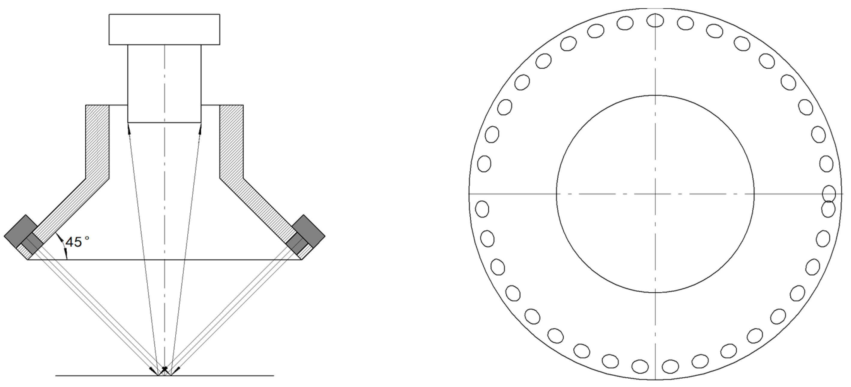
4.3. Calculation of Scanning-Path

The scanning of the large aperture spherical optical element is realized by the relative motion between the microscopic imaging system and the optical element, which is driven by the 5-axis motion system. As shown in Figure 4, point O serves as the center of the sphere, with point O′ as the apex of the sphere, and point O″ as the center of the yaw of the imaging system. The Δθ represents the yaw angle of the microscopic imaging system, while ΔX and ΔZ denote the relative displacement of the optical element in the X and Z directions, respectively. L signifies the distance between the center of the yaw of the imaging system and the object surface. Point A represents any point in the spherical optical element in the X direction, and point A′ denotes the target position to be moved to when point A severs as the scanning center point. By changing the yaw angle Δθ, the relative displacement ΔX and ΔZ of the camera scanning along the latitude line of the sphere is achieved. Furthermore, by rotating the optical element 360° around Z-axis, the camera can scan along the longitude of the sphere. Finally, the comprehensive scanning of spherical optical elements can be realized by alternating longitude and latitude scanning.
During the scanning process, the optical axis O′O″ of the microscopic imaging system must align with the center-to-curvature axis OA; the relationship between ΔZ, ΔX, and Δθ is given as follows. If the detection object is a convex lens, a summation operation is performed in the formula. Otherwise, if the detection object is a concave lens, a subtraction operation is performed in the formula.
ΔZ = L(1 − cosΔθ) ± R(1 − cosΔθ),
ΔX = LsinΔθ ± RsinΔθ

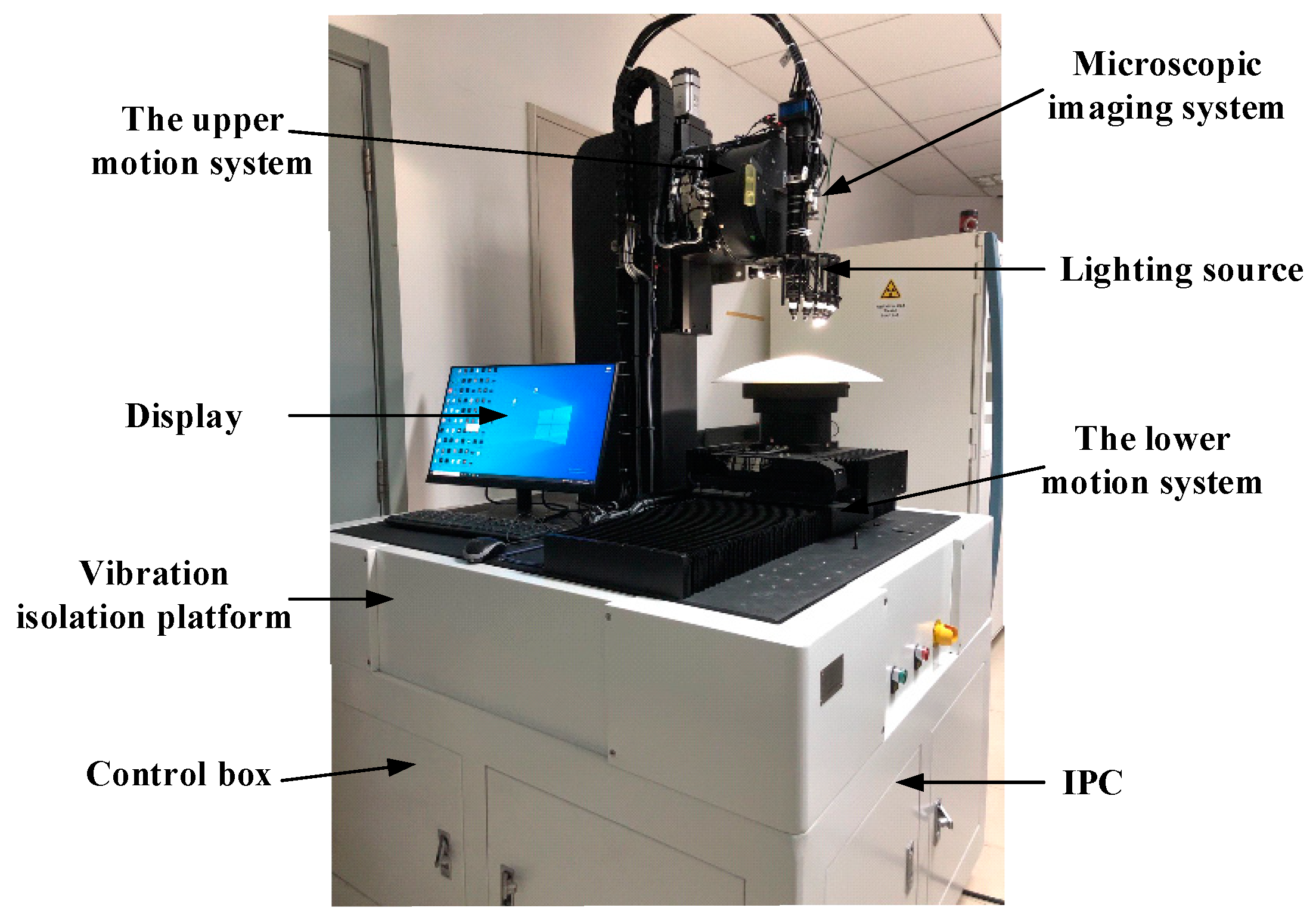
5. Platform Construction

The maximum aperture of the tested optical element is 400 mm, while the minimum relative aperture R/D value is 1. There are two types of defects to be inspected, such as scratch and pitting. The minimum width of scratch detectable is 2 µm, and the minimum diameter of pitting detectable is 4 µm.

5.1. Imaging System

Based on the imaging law for the minimum defect size under dark-field illumination, the image pixel equivalent is deduced to be 7 µm. Utilizing the scanning time calculation in Section 4.2, the larger the field of view of the imaging system, the smaller the total number of the sub-aperture for detecting the same optical element, and the shorter the scanning time. Therefore, a 25M large-array camera with a resolution of 5120 × 5120 pixels and a pixel size of 4.5 µm is chosen. Considering both the requirements of the imaging quality and accurate defect measurement, a 0.64×~4.5× automatic zoom lens with the depth of field range of 1.85 to 0.22 mm is selected. Then, an imaging system can be achieved with the sub-aperture chord length d of 35 mm and the corresponding arc angle φ of 5°.

5.2. Motion Scanning System

When the maximum aperture of the lens is 400 mm and the minimum R/D value is 1, the sag height H of the optical lens is about 53.6 mm and the arc angle β is 60 degrees according to the calculation method mentioned in Section 4.1 and Section 4.2. Given that the distance L between the offset center point of the imaging system and the object surface is 250 mm, the max travel distance Δθmax of the upper rotation axis is ±30 degrees(β/2), the max Z-axis travel distance ΔZmax is 108 mm, and the max X-axis travel distance ΔXmax is 400 mm according to the calculation method mentioned in Section 4.3. Therefore, the travel distances of X, Z, and Δθ are designed to be 500 mm, 200 mm, and ±45 degree.

5.3. Multi-Angle-Channel Illumination System

In order to accurately capture the defect images with the characteristics of different directions, sizes, and shapes, especially for weak scratches, a multi-angle-channel illumination system is designed to enhance the contrast between defects and background. A schematic diagram of a system with 36 channels of illumination is shown in Figure 5. Every channel of light is arranged with an interval of 5°along the optical axis of the imaging camera, while the angle between the light source and the optical axis is 45° from the perpendicular view to the optical axis. By controlling every channel of the light source dependently or multiply together, a multi-angle illumination can be obtained to collect more comprehensive defect information.

5.4. System Integration

The platform used for the defect detection instrument for curved surfaces is shown in Figure 6. The hardware system is implemented to realize high-resolution surface imaging, and is composed of the imaging system, the light source, the upper motion platform, the lower motion platform, the industrial personal computer, the control box, and the vibration isolation platform. The software Version 1.0 interface within the instrument is shown in Figure 7. The main functions of the software Version 1.0 system include image display, automatic detection, and process control, manual operation, system log, and statistical defect information.

6. Experiment

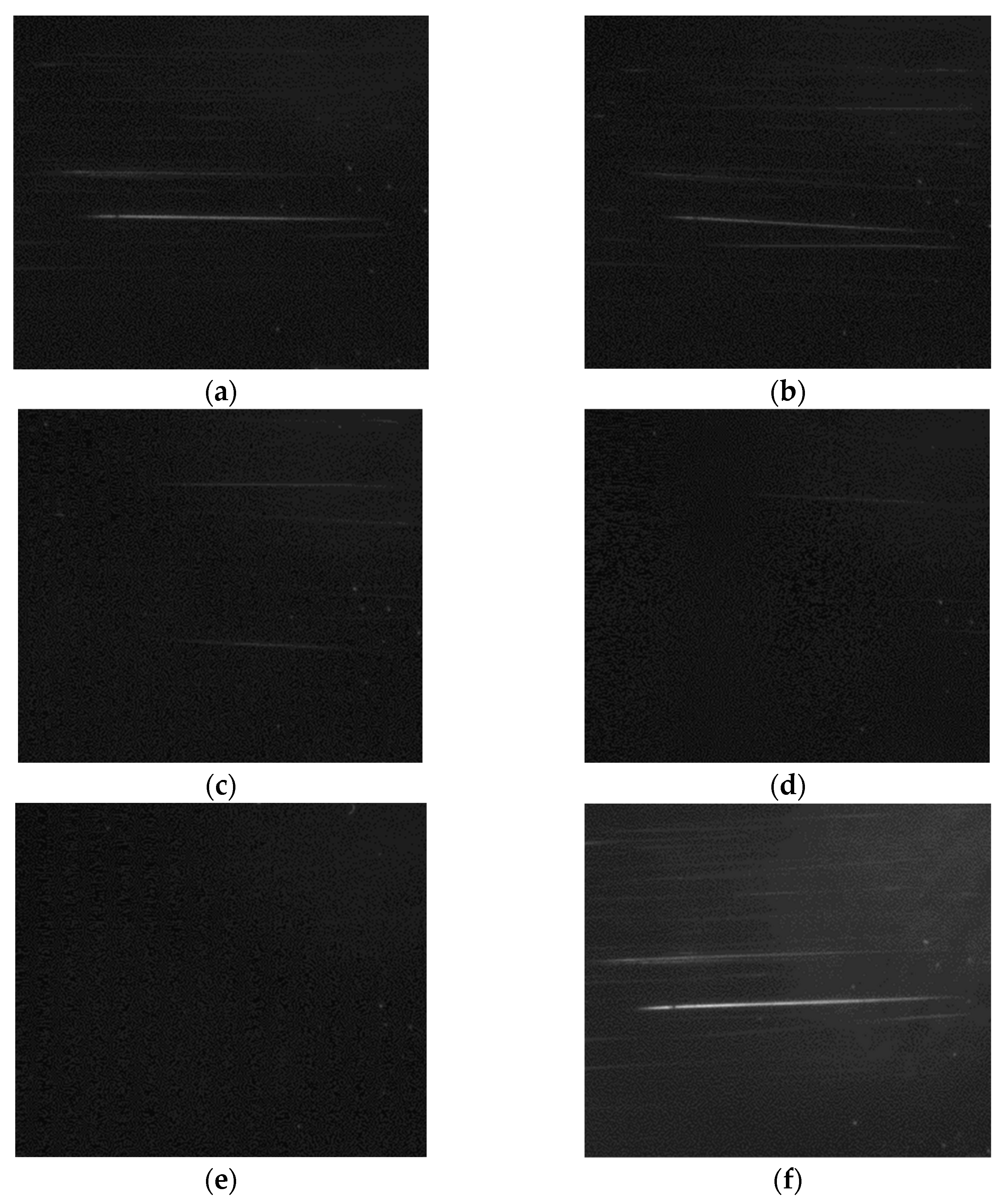
6.1. Defect Resolution Capability

To verify the defect resolution capability of the instrument, we designed and fabricated a standard glass calibration board with artificially etched patterns of varying sizes in elongated rectangular and circular dot shapes, simulating scratch and pitting defects. As shown in Figure 8, the scratch defect with a width of 1.3 µm and the defect with a diameter of 3.1 µm on the calibration board could be clearly distinguished. This means that the resolution performance of the optical imaging system meets the imaging requirements of 2 µm wide scratches and 4 µm pits.

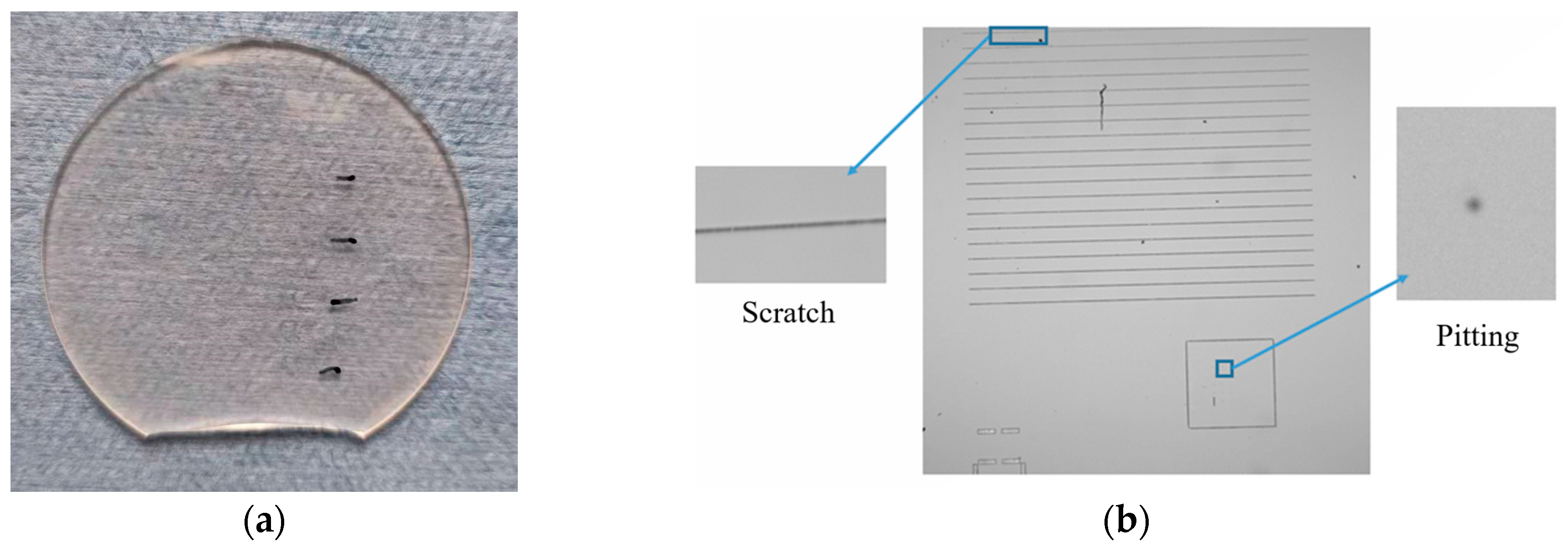
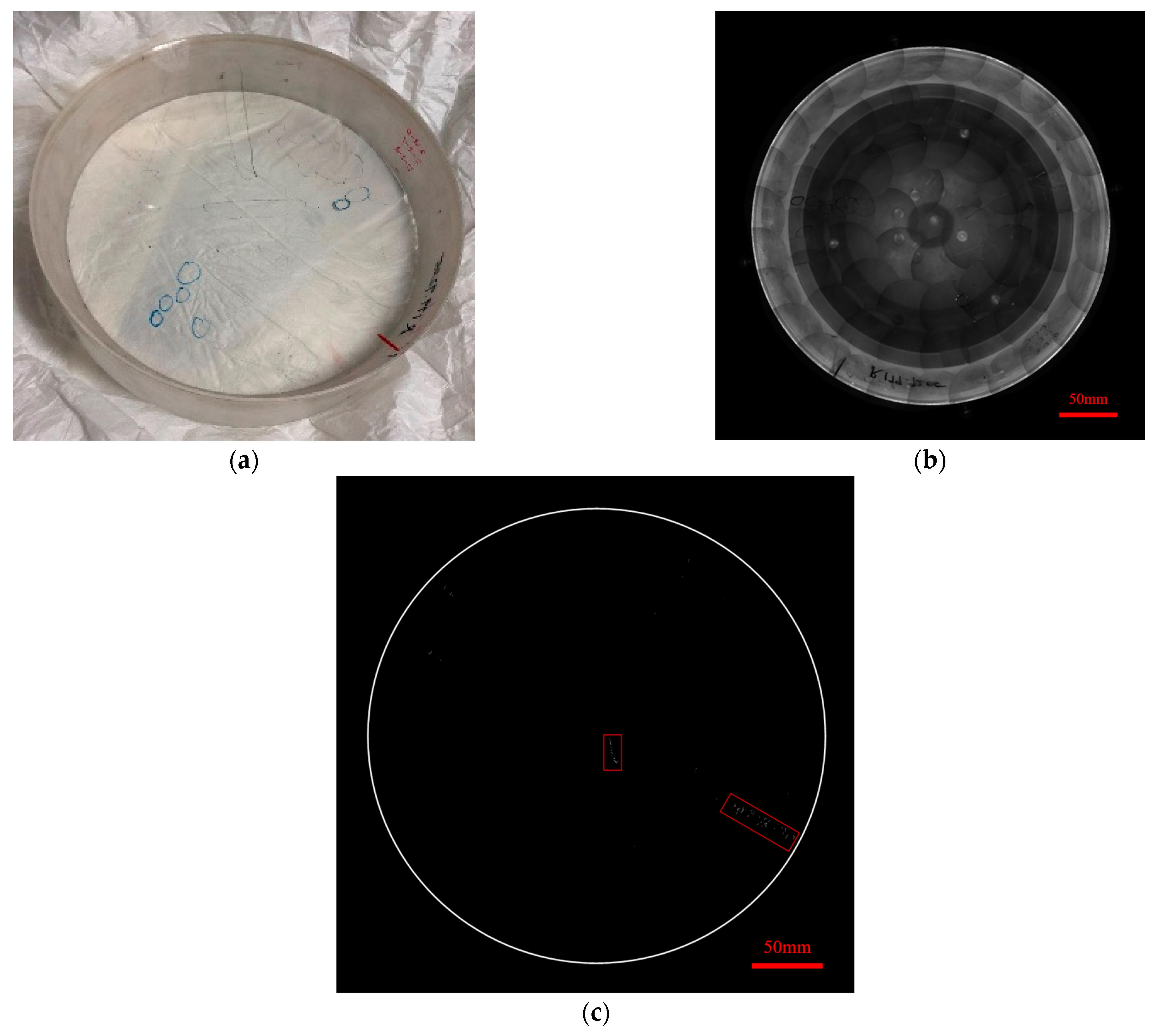
6.2. Image of Weak Scratch

By selecting a set of typical weak scratches on the optical surface for image experiment, we carried out a quality comparison between the images captured using single-angle illumination and by multi-angle illumination. As shown in Figure 9, a group of images of a weak scratch was collected under multi-angle illumination and single-angle illumination of 0 degrees, 2.5 degrees, 5 degrees, 7.5 degrees, and 10 degrees, respectively. As a result, the quality of the images of the weak scratch increases more significantly under the multi-angle illumination than under the single-angle illumination.

6.3. The Defect Detection Process and Experiment

A diagram of the automated detection process for optical surface defect is shown in Figure 10. Firstly, the optical element is mounted on the workbench, and the parameters of the curvature radius R and aperture D of the optical element were manually entered. Then, the brightness of the illumination source is set to match the requirements of the optical characteristics of the surface. After resetting the motion platform and automatically aligning the optical element, the microscopic imaging system is focused on the surface of the optical element. Finally, the remaining process is automatically completed, including surface scanning, image acquisition, defect detection, image stitching, result putout, and report generation.
As shown in Figure 11, a concave spherical lens with a diameter of 200 mm and an R/D ratio of 1 was selected to finish the experiment. About four bands of scanning with 68 images are required to cover the 200 mm diameter of the lens. Figure 11b displays the final image obtained by stitching the 68 sub-images together. Figure 11c presents a defect distribution map, where the defects are seen in a white color and the background is a black color (due to the small size of the white defect, the reduced defect image cannot be seen clearly. The areas where defects are more concentrated are indicated using red boxes). The adjustment time between annular rings is about 2 min, while the time required for single sub-aperture scanning and image capture is about 5 s. Therefore, 15 min are needed to complete the detection for a concave lens with a diameter of 200 mm. The processes of mage stitching, defect detection, and surface scanning are carried out simultaneously without occupying additional time.

7. Discussion

A detailed comparison between our study and other papers’ methods is shown in Table 1. It can be observed that detection methods for surface defects in planar optical elements are relatively mature, achieving a maximum defect resolution of 0.5 µm. The detection of large-diameter planar optical elements, measuring several hundred millimeters in size, can be accomplished within a duration of merely ten minutes. In contrast, research on surface defect detection in curved optical elements is relatively limited. G. Rosati [24] proposed an imaging method for curved surface defects, but did not consider the actual system design or conduct specific experiments. X. Tao [20] applied a robot as a scanning mechanism to detect 150 mm diameter curved surfaces but did not mention applicable curvature ranges or scanning detection times. Our paper systematically describes the overall design concept of the entire instrument, the design processes of each subsystem, thus offering a technical substratum for the engineering application of surface defect detection devices for curved optical elements. In the future, our project team plans to draw on the experience of defect detection in planar optical elements to further improve the instrument’s defect resolution and detection efficiency, aiming to replace manual inspection methods as soon as possible and achieve large-scale applications, thereby freeing inspection personnel from heavy workloads.

8. Conclusions

In this paper, an automatic surface defect detection instrument is proposed for large aperture curved optics. The overall design scheme, theoretical derivation, and calculation process of the instrument, as well as the detailed system hardware design scheme are introduced in detail. Based on the implemented platform, some relevant experiments are carried out. Our results demonstrate that the automatic defect detection instrument works well for spherical optical elements with a maximum diameter of 400 mm and R/D value of 1. The minimum scratch width that can be detected is 2 µm, and the minimum pitting diameter is 4 µm.
In addition, the imaging system and structural design of the defect detection instrument in this paper are fully applicable to large-aperture non-spherical optical elements. Subsequently, further research will be conducted on scanning path planning methods for non-spherical optical elements, especially quadric optical elements, to achieve surface defect detection.

Author Contributions

Conceptualization, Y.S. and M.Z.; methodology, Y.S.; software, M.L.; validation, Y.S., M.Z. and M.L.; formal analysis, M.Z.; investigation, Y.S.; resources, Y.S.; data curation, M.L.; writing—original draft preparation, Y.S.; writing—review and editing, M.Z.; visualization, M.Z.; supervision, M.Z.; project administration, Y.S.; funding acquisition, Y.S. All authors have read and agreed to the published version of the manuscript.

Funding

This research received no external funding.

Institutional Review Board Statement

Not applicable.

Informed Consent Statement

Not applicable.

Data Availability Statement

No new data were created.

Conflicts of Interest

The authors declare no conflict of interest.

References

  1. Fournier, J.; Grua, P.; Neauport, J.; Fargin, E.; Jubera, V.; Talaga, D.; DelGuerzo, A.; Raffy, G.; Jouannigot, S. Temperature dependence of luminescence for different surface flaws in high purity silica glass. Opt. Mater. Express 2013, 3, 1–10. [Google Scholar] [CrossRef]
  2. Zhao, Y.; Shao, J.; Liu, X.; Li, D. Tracking and understanding laser damage events in optics. High Power Laser Part. Beams 2022, 34, 011004-1–011004-12. [Google Scholar]
  3. Wang, L. Optical system of extreme ultraviolet lithography. Chin. J. Opt. Appl. Opt. 2010, 3, 453–461. (In Chinese) [Google Scholar]
  4. Ma, B.; Li, L.; Chang, J.; Du, B. Refractive Projection Lens for 90nm Resolution Lithography. Acta Opt. Sin. 2009, 29, 453–461. (In Chinese) [Google Scholar]
  5. Baker, L.R. Inspection of Surface Flaws by Comparator Microscopy. Appl. Opt. 1988, 27, 4620–4625. [Google Scholar] [CrossRef]
  6. Li, M.; Hou, X.; Zhao, W.; Wang, H.; Li, M.; Hu, X.; Zhao, Y.; Zhou, Y. Current situation and development trend of aspheric optical surface defect detection technology. Infrared Laser Eng. 2022, 51, 20220457-1–20220457-20. (In Chinese) [Google Scholar]
  7. Trivedia, V.; Joglekara, M.; Mahajan, S. Digital holographic imaging of refractive index distributions for defect detection. Opt. Laser Technol. 2019, 111, 439–446. [Google Scholar] [CrossRef]
  8. Falldorf, C.; Agour, M.; Kopylow, C.V. RB Bergmann. Phase retrieval for optical inspection of technical components. J. Opt. 2012, 14, 065701. [Google Scholar] [CrossRef]
  9. Zhou, H.; Hussain, M.M.R.; Banerjee, P.P. A review of the dual-wavelength technique for phase imaging and 3D topography. Light Adv. Manuf. 2022, 3, 314–334. [Google Scholar] [CrossRef]
  10. Khorin, P.A.; Volotovskiy, S.G.; Khonina, S.N. Optical detection of values of separate aberrations using a multi-channel filter matched with phase Zernike functions. Comput. Opt. 2021, 45, 525–534. (In Russian) [Google Scholar] [CrossRef]
  11. Khonina, S.N.; Khorin, P.A.; Serafimovich, P.G. Analysis of the wavefront aberrations based on neural networks processing of the interferograms with a conical reference beam. Appl. Phys. B 2022, 128, 60. [Google Scholar] [CrossRef]
  12. Khorin, P.A.; Dzyuba, A.P.; Chernykh, A.V. Neural Network-Assisted Interferogram Analysis Using Cylindrical and Flat Reference Beams. Appl. Sci. 2023, 13, 4831. [Google Scholar] [CrossRef]
  13. Choi, W.J.; Ryu, S.Y.; Kim, J.K.; Kim, J.Y.; Kim, D.U.; Chang, K.S. Fast mapping of absorbing defects in optical materials by full-field photothermal reflectance microscopy. Opt. Lett. 2013, 38, 4907–4910. [Google Scholar] [CrossRef]
  14. Sun, G.; Zhou, Z. Application of laser ultrasonic technique for non-contact detection of drilling-induced delamination in aeronautical composite components. Opt. Int. J. Light Electron Opt. 2014, 125, 3608–3611. [Google Scholar] [CrossRef]
  15. Lu, R.; Wu, A.; Zhang, T.; Wang, Y. Review on automated optical (visual) inspection and its applications in defect detection. Acta Opt. Sin. 2018, 38, 0815002. [Google Scholar]
  16. Lu, M.; Wang, Z.; Gao, P.; Guo, J. Defect detection and current situation of optical components. Opt. Instrum. 2020, 42, 88–94. [Google Scholar]
  17. Zhang, Z.; Xian, T.; Xu, D.; Feng, Z. Surface flaws detection algorithms for large aperture optical element. In Proceedings of the International Conference on Advanced Mechatronic Systems, Beijing, China, 22–24 August 2015. [Google Scholar]
  18. GB/T 41805-2022; Yang, Y.Y.; Cao, P.; Li, G.; Yang, L.M.; Liu, X. Methodology for the Quantitative Inspection of the Defect on Optics Surface—Microscopic Scattering Dark-Field Imaging. State Administration for Market Regulation, National Standardization Management Committee: Beijing, China, 2023.
  19. Zhang, Y.; Yang, Y.; Li, C.; Wu, F.; Chai, H.; Yan, K.; Zhou, L.; Li, Y.; Liu, D.; Bai, J.; et al. Defects evaluation system for spherical optical surfaces based on microscopic scattering dark-field imaging method. Appl. Opt. 2016, 55, 6162–6171. [Google Scholar] [CrossRef]
  20. Chen, X.; Li, J.; Sui, Y. A new stitching method for dark-field surface defects inspection based on simplified target-tracking and path correction. Sensors 2020, 20, 448. [Google Scholar] [CrossRef]
  21. Guo, S.; Lv, X.; Lu, Y. Research on defect detection of large-aperture multi-faceted optical components. In Proceedings of the SPIE of Applied Optics and Photonics, Beijing, China, 18 December 2023. [Google Scholar]
  22. Cao, P.; Yang, Y.; Li, C. Alignment methods for micron-scale surface defects automatic evaluation of large-aperture fine optics. Chin. Opt. Lett. 2015, 13, 041102. [Google Scholar]
  23. Tao, X.; Zhang, Z.T.; Zhang, F.; Xu, D. A Novel and Effective Surface Flaw Inspection Instrument for Large-Aperture Optical Elements. IEEE Trans. Instrum. Meas. 2015, 64, 2530–2540. [Google Scholar]
  24. Yin, Z.; Liu, H.; Zhao, L. Efficient and precise detection for surface flaws on large-aperture optics based on machine vision and machine learning. Opt. Laser Technol. 2023, 159, 109011. [Google Scholar] [CrossRef]
  25. Rosati, G.; Boschetti, G.; Biondi, A.; Rossi, A. Real-time defect detection on highly reflective curved surfaces. Opt. Lasers Eng. 2009, 47, 379–384. [Google Scholar] [CrossRef]
  26. Dong, J. Line-scanning laser scattering system for fast defect inspection of a large aperture surface. Appl. Opt. 2017, 56, 7089–7098. [Google Scholar] [CrossRef]
Figure 1. Principle of dark-field scattering microscopy imaging.
Photonics 11 00681 g001
Figure 2. Block diagram of the automatic defect detection instrument.
Photonics 11 00681 g002
Figure 3. Schematic diagram of the spherical surface parameters.
Photonics 11 00681 g003
Figure 4. Geometric relationship between microscopic imaging system and optical element. (Δ denotes the relative displacement of the optical element and the microscopic imaging system).
Photonics 11 00681 g004
Figure 5. Schematic diagram of the lighting source.
Photonics 11 00681 g005
Figure 6. Picture of the surface defect detection instrument.
Photonics 11 00681 g006
Figure 7. Software Version 1.0 interface of the surface defect detection instrument.
Photonics 11 00681 g007
Figure 8. Defect resolution capability detection. (a) Standard calibration board; (b) image of 1.3 µm scratch and 3.1 µm pitting on the board.
Photonics 11 00681 g008
Figure 9. Weak scratch imaging experiment. (a) Image of weak scratch under 0° illumination; (b) image of weak scratch under 2.5° illumination; (c) image of weak scratch under 5° illumination; (d) image of weak scratch under 7.5° illumination; (e) image of weak scratch under 10° illumination; (f) image of weak scratch under multi-angle illumination.
Photonics 11 00681 g009
Figure 10. Automatic defect detection process.
Photonics 11 00681 g010
Figure 11. Curved surface defect detection experiment. (a) optical element; (b) spliced images; (c) distribution map of defects.
Photonics 11 00681 g011
Table 1. Comparisons among various defect detection methods (N means not submitted in the paper).
MultimodalCurve Face or Planar
(C/P)
Sub Aperture Size
(mm)
Scanning Method
(Line/Area Scan)
Experiment Data
ApertureR/DMin Defect Size
(µm)
Time
(min)
OursYesC35AΦ200 mm1215
Paper [21]YesC6.6 × 4.4AΦ150 mmN0.5N
Paper [22]NoP2.3 × 2.3A320 × 320NNN
Paper [23]YesPNL810 × 460NN6
Paper [24]NoP50 × 50A430 × 430N106
Paper [25]NoCNANNNN
Paper [26]NoPNL810 × 450N0.514
Disclaimer/Publisher’s Note: The statements, opinions and data contained in all publications are solely those of the individual author(s) and contributor(s) and not of MDPI and/or the editor(s). MDPI and/or the editor(s) disclaim responsibility for any injury to people or property resulting from any ideas, methods, instructions or products referred to in the content.

