Review

Scanning Near-Field Optical Microscopy: Recent Advances in Disordered and Correlated Disordered Photonics

by
Nicoletta Granchi
European Laboratory for Nonlinear Spectroscopy, Department of Physics and Astronomy, University of Florence, 50019 Sesto Fiorentino, Italy
Photonics 2024, 11(8), 734; https://doi.org/10.3390/photonics11080734
Submission received: 28 June 2024 / Revised: 4 August 2024 / Accepted: 5 August 2024 / Published: 6 August 2024
(This article belongs to the Special Issue Advances in Near-Field Optics: Fundamentals and Applications)

Abstract

:
Disordered and correlated disordered photonic materials have emerged in the past few decades and have been rapidly proposed as a complementary alternative to ordered photonics. These materials have thrived in the field of photonics, revealing the considerable impact of disorder with and without structural correlations on the scattering, transport, and localization of light in matter. Scanning near-field optical microscopy (SNOM) has proven to be a fundamental tool for the study of the interaction between light and matter at the nanoscale in such systems, allowing for the investigation of optical properties and local electromagnetic fields with extremely high spatial resolution, surpassing the diffraction limit of conventional optical microscopy. In this review, the most important and recent advances obtained for disordered and correlated disordered luminescent structures by means of the aperture SNOM technique are addressed, showing how it allows the tailoring of local density of states (LDOS), as well as providing access to statistical analysis for multi-resonance disordered and hyperuniform disordered structures at telecom wavelengths.

1. Introduction

Periodic systems exhibiting perfect translational symmetries feature rotational symmetries in restricted numbers, while disordered and non-periodic structures support statistical isotropic characteristics that allow superior optical functionalities to be obtained. Light in disordered photonic materials can encounter diffusive and localization regimes thanks to random multiple scattering. This can offer powerful tools to control light–matter interactions and provide novel approaches in photonic applications. Photonic modes supported by such media exhibit resonances characterized by delimited spectral widths and extensions in space. Specifically, within transport models, light propagation in random photonic materials can be explained in terms of multiple elastic scattering. Electromagnetic waves undergo interference, giving rise to a localization regime whenever the mean free path of transport becomes on par with the wavelength, i.e., the rank of disorder is high enough [1,2]. This phenomenon, in which disorder determines the stoppage of electromagnetic transport and random shaped patterns of standing waves are generated, trapping light, is known as Anderson localization [3,4]. Thanks to the high spectral and spatial densities of Anderson modes, disordered materials can enlarge a plethora of potential applications thanks to the high degrees of freedom in the design. For this reason, disordered photonic materials based on scatterers that are randomly distributed have been envisioned in the field of telecommunications, quantum electrodynamics and renewable energies, as they can be exploited to stop, guide, and tightly confine light [5,6,7,8].
For these kinds of applications, imaging light localization at the nanoscale is a fundamental challenge. Over the years, the scanning near-field optical microscopy (SNOM) technique has been employed in nanophotonics research for the investigation of optical properties and detection of local electromagnetic fields with a subwavelength resolution, allowing researchers to explore nanoscale phenomena and to gain a deeper understanding of the interaction between light and matter at the nanoscale. SNOM has also been exploited not only for imaging purposes, but also for engineering and control over photonic resonances. Unlike Bloch modes in periodic systems, it is impossible to predict the precise formation of Anderson photonic resonances within a single disorder realization. Therefore, the deterministic control of selected random modes is also of major importance to compensate for the unavoidable disorder provided by the fabrication process, which determines deviations from nominal structures. Here, we report on how SNOM probes have proven to be an excellent tool to achieve the engineering [9,10] and mechanical tuning [5] of random photonic modes. The downside of luminescent disordered structures is that they support localized modes exhibiting relatively low quality factors ( 200), as experimentally detected [5,9,10]. Lately, a new and promising candidate displaying both the advantages of periodic and random systems is emerging in the field of photonics: hyperuniform disordered (HuD) media [11]. In this review, we therefore also show how SNOM spectroscopy has allowed, through a full characterization of light transport regimes in HuD media, the description of the features that elevate this class of correlated disorder materials as an ideal synthesis between ordered and disordered luminescent photonic systems, also revealing fascinating properties for the supported Anderson photonic modes, like robustness to fabrication-induced disorder.

2. Scanning Near-Field Optical Microscopy

All the results presented in this review were obtained by employing a commercial SNOM (Twinsnom, Omicron) employed in the configuration of illumination/collection. Scans over the surfaces of samples were performed by keeping the probe tip at a constant distance of a few tens of nanometers. In this way, spatially resolved optical maps can be acquired. In this setup, the sample is excited by a laser diode at 785 nm coupled to the tip which simultaneously collects the signal, that is dispersed by a spectrometer and revealed by a cooled InGaAs array. In every tip position, a spectrum is acquired with a spectral resolution of 0.1 nm. The estimated spatial resolution of the system is given by the area of collection of the SNOM tip, estimated to have a size of roughly 100 nm.

3. Near-Field Optical Microscopy of Disordered Photonic Structures

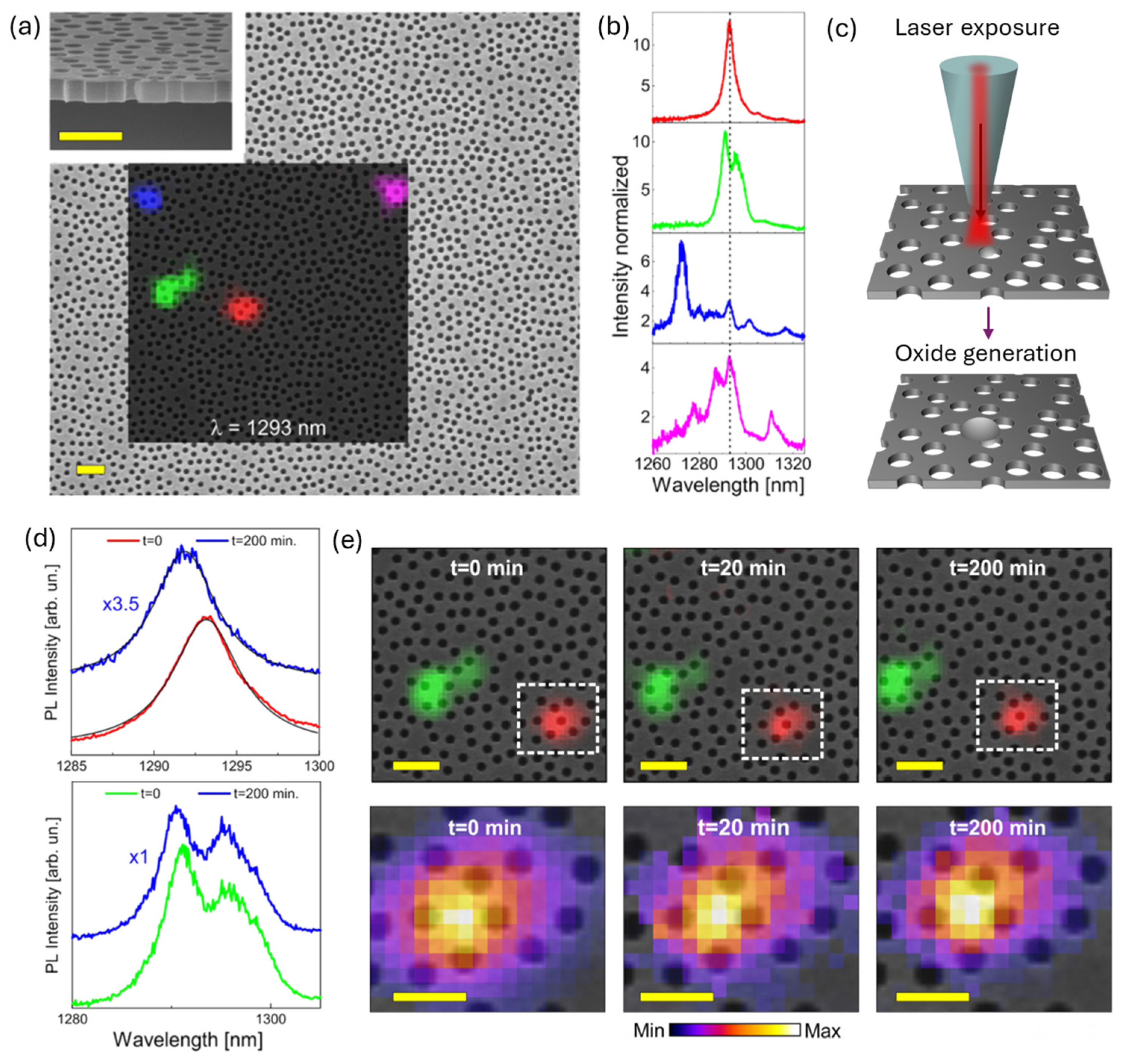
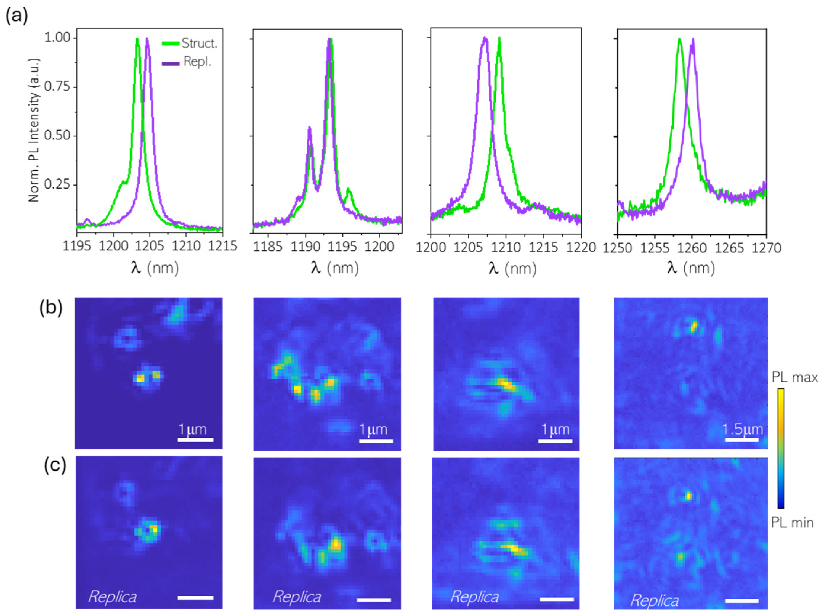
3.1. Engineering of Light Confinement in Random Dielectrics

One of the most significative advantages of random photonic systems is the small footprint, meaning the possibility to have a high spectral and spatial density of modes in a relatively small area. Indeed, in quantum cavity electrodynamics, the Purcell effect of a quantum emitter coupled to a random mode has allowed the limitations typical for photonic crystal nanocavity to be overcome, like the relatively large spatial extension of the photonic structure and the undetermined position of the emitters. It is possible to control the transport of light by imposing a selective excitation of modes available in the structure [12,13,14,15]; however, to actually exploit the potentialities of random systems, mode control is mandatory. It has been shown that it is theoretically possible to selectively tune isolated modes and even couple them to each other through a local fine modification of the dielectric structure [16,17]. Then, in the works of Refs. [9,10], it was experimentally proven with SNOM that it is possible to control the spectral features of an individual resonant mode in a 2D random photonic system. Moreover, the results obtained in [9] demonstrate the formation of artificially coupled states in a random platform by means of nano-oxidation, representing an important advance in the control of random modes. The samples under consideration are suspended GaAs membranes with embedded InAs QDs, acting as an optically active medium. These membranes are patterned with randomly distributed circular holes, as shown in the SEM images of Figure 1a. The SNOM hyperspectral imaging technique has been employed in [9,10] to demonstrate that random photonic patterns support Anderson localized modes in the near-infrared (telecom wavelength regime) range, which is relevant for many photonics utilizations. Photoluminescence (PL) intensity maps, evaluated at fixed wavelengths and overlapped with the SEM image in Figure 1a, reveal modes spatially localized in different regions, highlighted through hyperspectral imaging with different colors, with each corresponding to a single mode.
Figure 1b reports the SNOM-PL spectra corresponding to the four PL colored spots. Anderson modes can therefore be spectrally and spatially isolated well. In the laser-assisted non-thermal oxidation method [18], the SNOM tip is employed to locally alter the dielectric environment of the considered sample, as sketched in Figure 1c. This procedure allows for a smooth tuning of the resonant wavelength of any selected localized photonic mode. The tip was placed in correspondence of the maximum PL intensity (in this case λ = 1293 nm, red stain in Figure 1a) and the excitation laser was employed with a power of 1.45 mW. The photogenerated electron–hole pairs at the slab surface catalyze a regulated laser-assisted oxidation of the dielectric membrane. The illumination produces an oxide island on the sample while devouring the GaAs layer, and it spreads below and above the GaAs–air interface and in the holes, as represented in the sketch of Figure 1c. The oxidation effect on the photonic mode is a shift toward smaller wavelengths. Consequently, a smooth tuning of the random resonances is achieved through nanometric control over the oxide layers through the application of a mild laser excitation.
The first and final spectra of the random modes under investigation are reported in the two panels of Figure 1d (red and green in Figure 1a), respectively. The two modes have different tunings and are separated by 2 μm. This comparison has demonstrated that the oxidation process is local, and that the spectral line forms of the modes are unaffected by tuning.
Regarding the impact of tuning on the spatial features, the intricate comparison between light localization in disordered systems and photonic crystal properties has prompted researchers to consider whether a local perturbation of the disordered dielectric environment could alter the spatial distribution, extension, or location of the localized modes. By using near-field imaging of random modes as a function of the photo-induced oxidation duration, this question has been answered. The results are shown in Figure 1e, showing the PL intensity maps and the amplitude fitted with a Lorentzian line shape for the red mode at the initial, middle, and final tuning, corresponding to t = 0, 20, and 200 min. From these maps, it is clear that the three PL intensity maps are very similar, unveiling that the spatial distributions of randomly originated modes are not significantly affected by the local laser oxidation process. These findings made it possible to test other tuning techniques (such as liquid nano-infiltration, anodic oxidation, and dielectric deposition), previously developed in the field of photonic crystal cavities, on random materials. Reversible procedures were also envisaged in this context.

3.2. Nanoscale Mechanical Actuation with SNOM Tip on Random Modes

The possibility of designing and controlling target resonances in ordered and disordered photonic systems is of the utmost relevance not only to obtain the possibility of compensating for fabrication-induced disorder, which often results in unavoidable deviations with respect to the designed structure, but also to boost the sensitivity of devices used in realization (for example, novel integrated accelerometers [19] and high-precision mass sensors [20]). Specifically, in cavity quantum electrodynamics studies, controlling the exciton–photon coupling requires a spectrum tuning strategy that maintains all other mode properties. Different post-fabrication processing methods exploiting the SNOM tip, allowing the tuning of cavity resonances to compensate the fabrication-induced imperfections, have been developed in the last few decades [21], like liquid nano-infiltration [22] and nano-oxidation [18] (see the previous section for an example). Nevertheless, a lot of these methods are not always reversible, not suitable for large-scale applications, and eventually lead to both intrinsic and extrinsic optical degradation of the material, with emitter quenching or the Q factor lowering. Recently, a different approach, which relies on the coupling of modes in dual-layer photonic crystal membranes, has been proposed [23,24,25,26] and realized to achieve a reversible and fine but very large spectral tuning to specific target wavelengths through nanoscale mechanical actuation with the SNOM tip [5,26]. Using a mechanically reconfigurable bilayer photonic crystal resonator made up of two nominally identical photonic crystal cavities realized on two parallel membranes separated by a distance d 0 along the growth direction, this method takes advantage of the local forces that the near-field probe exerts on the resonator (see sketch of Figure 2a).
Temporal coupled mode theory provides an explanation for the physical idea that underlies the functionality of the device [27]. In fact, the degenerate original modes of the two membranes hybridize to form a pair of super-modes when the intermembrane distance is narrow enough for the out-of-plane evanescent field of one slab to permeate into the other. These retain the same in-plane geometry as the initial uncoupled modes after being delocalized over the two membranes. The initial photonic states divide into symmetric (S) and antisymmetric (AS) modes, which are analogous to the bonding and antibonding electronic wave functions of homoatomic molecules (Figure 2a). A perturbation (δd) of the upper membrane position caused by an external vertical force (δF) is directly transduced into the optical domain as a change in the splitting energy (δE) of the coupled modes as the coupling constant is dependent on the intermembrane distance ( d 0 ). The effect of the vertical local force exerted by the near-field probe is deformation of the upper membrane (see Figure 2b), which can be calculated by solving the static elastic equation in finite element method (FEM) simulations and that exhibit a parabolic dependence on the x-coordinate due to the boundary conditions. In correspondence with the cavity, the membrane’s core experiences the greatest distortion. Based on the applied force, this displacement is linear (Figure 2b) with an effective spring constant of 16 N/m. Figure 2c reports a record for the tuning of the double membrane L3 photonic molecule acquired when the SNOM probe exerts a compressive force on the device [26]. The sample consisted of two nominally 170 nm thick free-standing GaAs membranes. The photonic crystal pattern was etched through both membranes and consisted of a triangular array of holes (lattice constant a = 380 nm, filling ratio f = 0.32, holes radius r = 113 nm) (see the inset of Figure 2a). Three inline holes were cut out of the lattice to create a point-defect cavity (L3 cavity), and QDs are embedded in the upper membrane. The SNOM was employed in an illumination/collection geometry and in addition to applying a regulated local nN force, the dielectric tip was used as a near-field probe to collect the photoluminescence spectrum. In this configuration, the shear force approach is used to achieve control over the tip–surface separation. Step-by-step movement of the sample triggers the collection of the PL spectrum. Figure 2c shows the spectral dependence of modes AS and S (resulting from the coupling of the L3 fundamental mode) with respect to the variation of the z-position of the probe apex. This experiment’s total wavelength tuning for the z-range under investigation is 37.5 nm, which is more than three times larger than the record tuning obtained on devices of a similar nature utilizing electromechanical forces [28]. An analogue experiment was conducted over photonic modes supported by double membranes patterned with a random design (see Figure 2d) [5]. Depending on the vertical parity of the random modes in this system, a red or blue spectral shift can be produced by varying the air distance between the two membranes. A map of representative spectra for various upper membrane deformations and wavelengths is shown in Figure 2e. The spectra were taken at a fixed spatial position on the upper membrane. In a 250 nm diameter near-field spot, more than ten modes are detected. It is noteworthy that the shift may be precisely and reversibly manipulated across an extensive spectral range. In fact, one remarkable aspect of this methodology is the ability to precisely adjust the mode by a small amount of nm throughout a tuning range that surpasses λ = 30 nm. When compared to an atomic force microscopy (AFM) tip, for example, the use of a SNOM tip has the advantage of enabling the mechanical modification of the double membrane system while also allowing one to investigate the optical effect of this modification on all random modes that exhibit some spatial extension below the tip. Remarkably, this made it possible to note that the spectrum tuning is accomplished without altering the modes’ spatial distribution, which answers the need to match the random mode with an emitter.

4. Light Transport Regimes and Localization in Hyperuniform Disordered Photonic Systems

Since traditional optical systems inevitably fail to distinguish sub-micrometric details of such nanostructures, the SNOM technique is the eligible candidate to overcome this problem. It can conveniently map the electric field in proximity to photonic nanostructures with a sub-wavelength spatial resolution and finely tune their resonances. After the theoretical prediction of Koenderink et al. in 2005 [29], Intonti et al. (2008) showed that the precise resonance frequency tuning of a photonic crystal cavity on slab may be achieved locally by introducing a sub-wavelength dielectric SiO2 tip without necessarily causing large losses [30]. The electromagnetic local density of states (LDOS), which is necessary for the accurate characterization of photonic structure in general, can be powerfully mapped using the same methodology [31,32,33]. The technique of SNOM hyperspectral imaging has been applied not only to the investigation and engineering of purely random photonic modes, as shown in Section 3. As a matter of fact, although random systems are worth the numerous investigations due to the advantages of high spectral and spatial density exhibited in small footprints, their Q -factors are rather low, ranging from 200 to 400. Recently, there has been an increasing interest in disordered dielectric materials having structural correlations, which bridge the gap between completely ordered photonic crystals and random structures [34]. These materials include HuD photonic systems as a particular class [11]. These systems have recently been shown to display large isotropic photonic band gaps (PBG), as well as optical transparency, to mention two of the most fascinating and promising features [35,36]. In particular, HuD systems may show PBGs comparable in width to the ones found in photonic crystals, because of the point pattern template that serves as the foundation for the structures. A point pattern in real space is considered hyperuniform if, within a spherical window of observation of radius R , the number variance σ ( R ) 2 , given a large R , rises more slowly than the window volume, that is, more slowly than R d (in d dimensions). This indicates that transparency at long wavelengths is caused by the structural factor, S ( k ) , approaching zero in Fourier space as k 0. Among the several experimental photonic realizations of HuD structures [37,38,39,40], there was still a lack of a thorough description of luminous HuD structures in the optical range. This challenge was tackled in the experiments presented in Refs. [41,42,43] by creating the first optically active hyperuniform network on a membrane with quantum dots embedded in the middle and emitting at telecom wavelength through design and nanofabrication (SEM image in Figure 3a). The optical near-field hyperspectral imaging of HuD systems constituted a breakthrough in the field, which produced a number of novel and surprising findings on the quirks of HuD modes.
The recorded near-field spectrum was divided by one of the QDs to determine the PL enhancement spectrum for each tip position in order to gain insight into the nature of the photonic modes (reported in the inset of Figure 3a). Figure 3b displays a typical SNOM PL enhancement spectrum obtained at a particular probe point. It displays resonances that are sparsely distributed across the QDs’ entire emission spectrum. By doing this for every tip position during the SNOM scan, i.e., for every pixel of the map, it was possible to reconstruct the near-field spatial distribution of the PL enhancement over a broad range of wavelengths (1165–1265), as shown in Figure 3c. This map is collective, meaning that each bright spot represents the brightest mode (or superposition of modes) in that spatial region within the chosen spectral window. It is neither a single-mode map nor a map at a single emission frequency. It allows one to observe that the many resonances spread all over the selected spectral region also spatially occur all over the structure and can therefore be used as an indication of the position of the localized mode. To study the single modes in detail, the SNOM hyperspectral maps can also be filtered around a single peak wavelength. Following the principle illustrated in the sketch of Figure 3c, for example, it is possible to acquire a spectrum in correspondence of the point in which the mode displays the maximum intensity, like what has been done in Figure 3d for modes 1, 2, and 3. Then, the SNOM hyperspectral map can be filtered around the central wavelengths of the corresponding peaks to obtain the single maps reported in Figure 3e, thanks to which the submicrometric details of the modes can be observed. Interestingly, the three modes of Figure 3e are Anderson modes located at the lower PBG edge. Through the SNOM experiment, it was also possible to report on the statistical properties of all the modes in the structure. Figure 3f reports the number of modes detected in an 8 µ m × 8 µ m scan by dividing the spectral range into six intervals. The experimental data nicely agree with the trend of the number of modes extracted from FEM simulations and clearly define three main regions according to theoretical predictions. In region 1 (1100–1160 nm), no modes are detected due to the presence of the PBG with no detected modes. Around 1160 nm, the first resonances are seen, with strongly localized field profiles similar to those in Figure 3e. All modes in region 2 (1160–1195 nm) have this property. Following a transition zone (1195–1225 nm), the modes then exhibit a delocalization throughout the entire structure as the wavelength is increased, and this region is labeled as region 3 ( λ > 1225 nm).
The spatial extent of the HuD modes can be directly accessed using near-field imaging, which makes it possible to examine the specifics of the localized-to-delocalized mode transition close to the dielectric band edge. This is measurable quantitatively by calculating the inverse participation ratio (IPR) [44,45]. Figure 3g shows the trends of the theoretical (purple) and experimental (red) calculations of the HuD modes with respect to the wavelength λ , which confirm the presence of the three spectral regions characterized by different light transport regimes. The transition from Anderson localization (region 2), characterized by high values of IPR, to a diffusive regime characterized by values of IPR near 1 (region 3), happens in an intermediate spectral region in which localized and delocalized modes coexist and is further confirmed by the analysis of the Q factor trend reported in Figure 3f. As predicted by theory, HuD Anderson modes, when confined and near the PBG, may exhibit high quality factors; however, for protracted modes further from the band edge, Q drops. Through this analysis, it was possible to demonstrate that HuD photonic systems on a slab display a high spectral and spatial density of modes in a small footprint. Many of these are localized Anderson modes with Q/V ratio comparable to those found in standard photonic crystal cavities, making HuD systems a promising platform that combines the advantages of both random and ordered photonics.
In light of the exploitability of modes in optoelectronic applications, large Q/V ratios are not the only crucial feature to consider. An entire area of optoelectronic research has been driven by the predictability of photonic modes, with the goal of enabling post-fabrication compensation of disorder induced by fabrication as well as deterministic control of random modes on top of an unpredictable spatial distribution (see Section 3.1 and Section 3.2). Recently, it was reported that Anderson modes located at the PBG edge of HuD luminescent samples are more robust against local perturbations and fabrication-induced disorder with respect to their disordered and ordered counterparts [41,43]. Undoubtedly, potential flaws that could reduce the optical performance of photonic crystal devices have less of an impact on hyperuniform structures that are disordered, which eases manufacturing restrictions. This can be observed in the results shown in Figure 4, that were obtained by performing SNOM measurements on two nominally identical samples that are labeled as Structure and Replica.
The two replicas are investigated in the near-field demonstrating that the same modes can be spotted in the two structures. Some examples of the reproducible modes are given in Figure 4. The PL enhancement spectra obtained in the replica (in green) at the location of the PL signal’s maximum intensity for the chosen mode are reported in Figure 4a and are contrasted with their corresponding spectra in the original structure (in purple).
Correspondingly, the panels of Figure 4b show the SNOM PL enhancement maps acquired at the central wavelengths of the green peaks in the nominal structure. Rather, the SNOM PL maps obtained at the center wavelengths of the blue peaks from the Replica are displayed in Figure 4c. For each of the four modes under consideration, there is a clear consistency in the submicrometric features of the most changeable forms in the replicas’ field distributions, both in the brightest areas and in the zones with lower signal.
It should be noted that the fourth mode corresponds to a spectral region where the diffusive regime is dominating, whereas the previous three modes can be thought of as localized. In actuality, the localization scale of modes plays a significant role in assessing the impact of disorder. Thanks to this kind of analysis, which was reported in Refs. [41,43], conclusions can be drawn regarding the strength of Anderson-localized modes in HuD whose spatial extension happens on a scale that is smaller with respect to that of fabrication-induced disorder, as well as the fact that delocalized modes share the same property. We can therefore state that, within the context of optical confinement applications, it has been widely shown that, by means of SNOM hyperspectral experiments, HuD geometry can provide important advantages in photonic structures. However, HuD materials not only exhibit large band gaps enabled by the hyperuniform geometrical characteristics of the underlying point pattern template upon which the structures are constructed [35], but they also induce a resultant statistical isotropy in the photonic characteristics of the dielectric structures due to the intrinsic geometrical statistical isotropy of these patterns. This has significant importance for a range of photonic functions, as their ability to comply with broad boundary restrictions can offer a versatile optical insulator framework for planar optical circuits [46]. Consequently, the concept of optical cavities in HuD photonic materials, which was proposed in Refs. [47,48], provided a path that may overcome many of the obstacles in the realm of optical cavities and open up a number of options for further experimental research. This task was accomplished in Ref. [42], where the design and fabrication of optical cavities in HuD photonic networks on a slab was carried out, along with a full SNOM characterization of their properties. Figure 5a shows the SEM top view image of an engineered cavity embedded in the HuD network [42], in which the seven modified holes are visible. The combination of the near-field hyperspectral imaging technique with the topographic imaging of the samples (Figure 5b) was exploited to align the different maps of each resonant mode at the nanoscale. The engineered cavity supports many resonances with a multipolar character. In the typical SNOM PL spectrum reported in Figure 5c, we can spot four peaks that correspond to the first four cavity resonances, labeled in order of decreasing energy: octupole-like (O), hexapole-like (H), quadrupole-like (Q), and dipole-like (D) [49]. From FEM simulations, it is possible to calculate the electric field intensity distributions of the first four modes, as shown in Figure 5d. Paired with the SNOM optical maps, the morphological information provided by the SNOM topography has allowed the determination that the four resonances in Figure 5c’s spectrum match the four cavity modes that the theoretical study predicted. A single Lorentzian fit was performed for each peak in the PL spectrum in order to accurately determine the LDOS spatial distribution of each cavity resonance and reconstruct the spectral shift maps [30] caused by the SNOM tip (overlapped in transparency with the sample’s SEM image and reported in Figure 5e). It is possible to determine if the submicrometric features of the design are accurately recreated by comparing the FEM simulated maps of the electric field intensity distribution (presented in Figure 5d) with the experimentally inferred spectral shift maps.
Because of the spatial isotropy of the HuD environment, these deterministic modes coexisting with Anderson-localized modes are a viable alternative for implementation in optoelectronic devices.

5. Conclusions

After the invention of super-resolution techniques, a great achievement awarded with the Nobel Prize in Chemistry in 2014 and allowing extremely high spatial resolution in standard microscopy, SNOM might seem like a surpassed method. This is not true, since nowadays the aim of SNOM is the understanding of light–matter interaction at the nanoscale. Indeed, it is the near-field component of the electromagnetic field that dominates processes like absorption, emission, scattering, non-linear optics, etc., at the level of a single quantum source. Many research activities on disordered and correlated disordered media have bloomed in the context of photonics and have unveiled the impact of structural correlations on the ways in which light is scattered, transported and localized in matter. This review has shown how SNOM is nowadays a relevant tool for highlighting the important and sometimes subtle aspects of light–matter interaction, not only for being a powerful imaging technique capable of providing essential and precious physical information at the nanoscale, but also for tailoring the LDOS of microresonators and providing access to statistical analysis in multi-resonance structures at telecom wavelengths. Thanks to the great potential of this technique, many other exciting routes will be paved in advanced nanophotonic applications, where sub-wavelength resolution imaging will play fundamental roles that are yet to be explored.

Funding

This research was funded by PNRR project I-PHOQS (CUP B53C22001750006).

Institutional Review Board Statement

Not applicable.

Informed Consent Statement

Not applicable.

Data Availability Statement

Not applicable.

Acknowledgments

The author acknowledges Francesca Intonti and Massimo Gurioli for their helpful discussions and support.

Conflicts of Interest

The author declares no conflicts of interest.

References

  1. Sheng, P. Introduction to Wave Scattering. In Localization and Mesoscopic Phenomena, 2nd ed.; Academic: San Diego, CA, USA, 2000. [Google Scholar]
  2. Riboli, F.; Uccheddu, F.; Monaco, G.; Caselli, N.; Intonti, F.; Gurioli, M.; Skipetrov, S.E. Tailoring Correlations of the Local Density of States in Disordered Photonic Materials. Phys. Rev. Lett. 2017, 119, 043902. [Google Scholar] [CrossRef] [PubMed]
  3. Anderson, P.W. Absence of Diffusion in Certain Random Lattices. Phys. Rev. 1958, 109, 1492–1505. [Google Scholar] [CrossRef]
  4. Wiersma, D.; Bartolini, P.; Lagendijk, A.; Righini, R. Localization of light in a disordered medium. Nature 1997, 390, 671–673. [Google Scholar] [CrossRef]
  5. Balestri, D.; Petruzzella, M.; Checcucci, S.; Intonti, F.; Caselli, N.; Sgrignuoli, F.; van Otten, F.W.M.; Fiore, A.; Gurioli, M. Mechanical and Electric Control of Photonic Modes in Random Dielectrics. Adv. Mater. 2019, 31, 1807274. [Google Scholar] [CrossRef] [PubMed]
  6. Mafi, A.; Karbasi, S.; Koch, K.W.; Hawkins, T.; Ballato, J. Transverse Anderson Localization in Disordered Glass Optical Fibers: A Review. Materials 2014, 7, 5520–5527. [Google Scholar] [CrossRef] [PubMed]
  7. Froufe-Pérez, L.S.; Engel, M.; Sáenz, J.J.; Scheffold, F. Band gap formation and Anderson localization in disordered photonic materials with structural correlations. Proc. Natl. Acad. Sci. USA 2017, 114, 9570–9574. [Google Scholar] [CrossRef] [PubMed]
  8. Sapienza, L.; Thyrrestrup, H.; Stobbe, S.; Garcia, P.D.; Smolka, S.; Lodahl, P. Cavity quantum electrodynamics with Anderson localized modes. Science 2010, 327, 1352. [Google Scholar] [CrossRef] [PubMed]
  9. Riboli, F.; Caselli, N.; Vignolini, S.; Intonti, F.; Vynck, K.; Barthelemy, V.M.P.; Gerardino, A.; Balet, L.P.; Li, L.H.; Fiore, A.; et al. Engineering of light confinement in strongly scattering disordered media. Nat. Mater. 2014, 13, 720–725. [Google Scholar] [CrossRef] [PubMed]
  10. Caselli, N.; Riboli, F.; Intonti, F.; La China, F.; Biccari, F.; Gerardino, A.; Gurioli, M. Spatial steadiness of individual disorder modes upon controlled spectral tuning. APL Photonics 2016, 1, 041301. [Google Scholar] [CrossRef]
  11. Torquato, S.; Stillinger, F.H. Local density fluctuations, hyperuniformity, and order metrics. Phys. Rev. E 2003, 68, 041113. [Google Scholar] [CrossRef]
  12. Redding, B.; Liew, S.; Sarma, R.; Cao, H. Compact spectrometer based on a disordered photonic chip. Nat. Photonics 2013, 7, 746–751. [Google Scholar] [CrossRef]
  13. Ching, E.; Leung, P.; Maassen van den Brink, A.; Suen, W.; Tong, S.; Young, K. Quasinormal-mode expansion for waves in open systems. Rev. Mod. Phys. 1998, 70, 1545–1554. [Google Scholar] [CrossRef]
  14. Noginov, M.; Dewar, G.; McCall, M.; Zheludev, N. Tutorials in Complex Photonic Media; SPIE: Bellingham, WA, USA, 2010; Chapter 9. [Google Scholar]
  15. Popoff, S.; Lerosey, G.; Carminati, R.; Fink, M.; Boccara, A.; Gigan, S. Measuring the Transmission Matrix in Optics: An Approach to the Study and Control of Light Propagation in Disordered Media. Phys. Rev. Lett. 2010, 104, 0601. [Google Scholar] [CrossRef] [PubMed]
  16. Labonté, L.; Vanneste, C.; Sebbah, P. Localized mode hybridization by fine tuning of two-dimensional random media. Opt. Lett. 2012, 37, 1946–1948. [Google Scholar] [CrossRef]
  17. Vanneste, C.; Sebbah, P. Complexity of two-dimensional quasimodes at the transition from weak scattering to Anderson localization. Phys. Rev. A 2009, 79, 1802. [Google Scholar] [CrossRef]
  18. Intonti, F.; Caselli, N.; Vignolini, S.; Riboli, F.; Kumar, S.; Rastelli, A.; Schmidt, O.G.; Francardi, M.; Gerardino, A.; Balet, L.; et al. Mode tuning of photonic crystal nanocavities by photoinduced non-thermal oxidation. Appl. Phys. Lett. 2012, 100, 033116. [Google Scholar] [CrossRef]
  19. Krause, A.G.; Winger, M.; Blasius, T.D.; Lin, Q.; Painter, O. A high-resolution microchip optomechanical accelerometer. Nat. Photonics 2012, 6, 768. [Google Scholar] [CrossRef]
  20. Liu, F.; Alaie, S.; Leseman, Z.C.; Hossein-Zadeh, M. Sub-pg mass sensing and measurement with an optomechanical oscillator. Opt. Express 2013, 21, 19555. [Google Scholar] [CrossRef] [PubMed]
  21. Faraon, A.; Vučković, J. Local temperature control of photonic crystal devices via micron-scale electrical heaters. Appl. Phys. Lett. 2009, 95, 043102. [Google Scholar] [CrossRef]
  22. Intonti, F.; Vignolini, S.; Riboli, F.; Zani, M.; Wiersma, D.S.; Balet, L.; Li, L.H.; Francardi, M.; Gerardino, A.; Fiore, A.; et al. Tuning of photonic crystal cavities by controlled removal of locally infiltrated water. Appl. Phys. Lett. 2009, 95, 173112. [Google Scholar]
  23. Suh, W.; Yanik, M.F.; Solgaard, O.; Fan, S. Displacement-sensitive photonic crystal structures based on guided resonance in photonic crystal slabs. Appl. Phys. Lett. 2003, 82, 1999. [Google Scholar] [CrossRef]
  24. Midolo, L.; van Veldhoven, P.J.; Dundar, M.A.; Notzel, R.; Fiore, A. Electromechanical wavelength tuning of double-membrane photonic crystal cavities. Appl. Phys. Lett. 2011, 98, 211120. [Google Scholar] [CrossRef]
  25. Granchi, N.; Petruzzella, M.; Balestri, D.; Fiore, A.; Gurioli, M.; Intonti, F. Multimode photonic molecules for advanced force sensing. Opt. Express 2019, 27, 37579–37589. [Google Scholar] [CrossRef] [PubMed]
  26. Petruzzella, M.; La China, F.; Intonti, F.; Caselli, N.; De Pas, M.; van Otten, F.W.M.; Gurioli, M.; Fiore, A. Nanoscale mechanical actuation and near-field read-out of photonic crystal molecules. Phys. Rev. B 2016, 94, 115413. [Google Scholar] [CrossRef]
  27. Haus, H.A.; Huang, W.P.; Kawakami, S.; Whitaker, N.A. Coupled-mode theory of optical waveguides. J. Light. Technol. 1987, 5, 16. [Google Scholar] [CrossRef]
  28. Midolo, L.; Pagliano, F.; Hoang, T.B.; Xia, T.; van Otten, F.W.M.; Li, L.H.; Linfield, E.H.; Lermer, M.; Hofling, S.; Fiore, A. Spontaneous emission control of single quantum dots by electromechanical tuning of a photonic crystal cavity. Appl. Phys. Lett. 2012, 101, 091106. [Google Scholar] [CrossRef]
  29. Koenderink, A.F.; Kafesaki, M.; Buchler, B.C.; Sandoghdar, V. Controlling the Resonance of a Photonic Crystal Microcavity by a Near-Field Probe. Phys. Rev. Lett. 2005, 95, 153904. [Google Scholar] [CrossRef]
  30. Intonti, F.; Vignolini, S.; Riboli, F.; Vinattieri, A.; Wiersma, D.S.; Colocci, M.; Balet, L.; Monat, C.; Zinoni, C.; Li, L.H.; et al. Spectral tuning and near-field imaging of photonic crystal microcavities. Phys. Rev. B 2008, 78, 041401(R). [Google Scholar] [CrossRef]
  31. Louvion, N.; Gérard, D.; Mouette, J.; de Fornel, F.; Seassal, C.; Letartre, X.; Rahmani, A.; Callard, S. Local Observation and Spectroscopy of Optical Modes in an Active Photonic-Crystal Microcavity. Phys. Rev. Lett. 2005, 94, 113907. [Google Scholar] [CrossRef]
  32. Kramper, P.; Kafesaki, M.; Soukoulis, C.M.; Birner, A.; Müller, F.; Gösele, U.; Wehrspohn, R.B.; Mlynek, J.; Sandoghdar, V. Near-field visualization of light confinement in a photonic crystal microresonator. Opt. Lett. 2004, 29, 174. [Google Scholar] [CrossRef]
  33. Volkov, V.S.; Bozhevolnyi, S.I.; Borel, P.I.; Frandsen, L.H.; Kristensen, M. Near-field characterization of low-loss photonic crystal waveguides. Phys. Rev. B 2005, 72, 035118. [Google Scholar] [CrossRef]
  34. Vynck, K.; Pierrat, R.; Carminati, R.; Froufe-Pérez, L.S.; Scheffold, F.; Sapienza, R.; Vignolini, S.; Sáenz, J.J. Light in correlated disordered media. Rev. Mod. Phys. 2023, 95, 045003. [Google Scholar] [CrossRef]
  35. Florescu, M.; Torquato, S.; Steinhardt, P.J. Designer disordered materials with large, complete photonic band gaps. Proc. Natl. Acad. Sci. USA 2009, 106, 20658–20663. [Google Scholar] [CrossRef] [PubMed]
  36. Leseur, O.; Pierrat, R.; Carminati, R. High-density hyperuniform materials can be transparent. Optica 2016, 3, 763–767. [Google Scholar] [CrossRef]
  37. Muller, N.; Haberko, J.; Marichy, C.; Scheffold, F. Silicon hyperuniform disordered photonic materials with a pronounced gap in the shortwave infrared. Adv. Opt. Mater. 2014, 2, 115–119. [Google Scholar] [CrossRef]
  38. Castro-Lopez, M.; Gaio, M.; Sellers, S.; Gkantzounis, G.; Florescu, M.; Sapienza, R. Reciprocal space engineering with hyperuniform gold disordered surfaces. APL Photonics 2017, 2, 061302. [Google Scholar] [CrossRef]
  39. Aubry, G.J.; Froufe-Pérez, L.S.; Kuhl, U.; Legrand, O.; Scheffold, F.; Mortessagne, F. Experimental Tuning of Transport Regimes in Hyperuniform Disordered Photonic Materials. Phys. Rev. Lett. 2020, 125, 127402. [Google Scholar] [CrossRef] [PubMed]
  40. Razo-López, L.A.; Aubry, G.J.; Pinheiro, F.A.; Mortessagne, F. Strong localization of microwaves beyond two dimensions in aperiodic Vogel spirals. Phys. Rev. B 2024, 109, 014205. [Google Scholar] [CrossRef]
  41. Granchi, N.; Spalding, R.; Lodde, M.; Petruzzella, M.; Otten, F.W.; Fiore, A.; Intonti, F.; Sapienza, R.; Florescu, M.; Gurioli, M. Near-Field Investigation of Luminescent Hyperuniform Disordered Materials. Adv. Opt. Mater. 2022, 10, 2102565. [Google Scholar] [CrossRef]
  42. Granchi, N.; Lodde, M.; Stokkereit, K.; Spalding, R.; van Veldhoven, P.J.; Sapienza, R.; Fiore, A.; Gurioli, M.; Florescu, M.; Intonti, F. Near-field imaging of optical nanocavities in hyperuniform disordered materials. Phys. Rev. B 2023, 107, 06420. [Google Scholar] [CrossRef]
  43. Granchi, N.; Spalding, R.; Stokkereit, K.; Lodde, M.; Petruzzella, M.; Otten, F.V.; Sapienza, R.; Fiore, A.; Florescu, M.; Intonti, F. High spatial resolution imaging of light localization in hyperuniform disordered patterns of circular air pores in a dielectric slab. Front. Photonics 2023, 4, 1199411. [Google Scholar] [CrossRef]
  44. Imagawa, S.; Edagawa, K.; Morita, K.; Niino, T.; Kagawa, Y.; Notomi, M. Photonic band-gap formation, light diffusion, and localization in photonic amorphous diamond structures. Phys. Rev. B 2010, 82, 115116. [Google Scholar] [CrossRef]
  45. Yuan, T.; Feng, T.; Xu, T. Manipulation of transmission by engineered disorder in one-dimensional photonic crystals. Opt. Express 2019, 27, 6483–6494. [Google Scholar] [CrossRef] [PubMed]
  46. Milosevic, M.M.; Man, W.; Nahal, G.; Steinhardt, P.J.; Torquato, S.; Chaikin, P.M.; Amoah, T.; Yu, B.; Mullen, R.A.; Florescu, M. Hyperuniform disordered waveguides and devices for near infrared silicon photonics. Sci. Rep. 2019, 9, 20338. [Google Scholar] [CrossRef] [PubMed]
  47. Florescu, M.; Steinhardt, P.J.; Torquato, S. Optical cavities and waveguides in hyperuniform disordered photonic solids. Phys. Rev. B 2013, 87, 165116. [Google Scholar] [CrossRef]
  48. Amoah, T.; Florescu, M. High-Q optical cavities in hyperuniform disordered materials. Phys. Rev. B 2015, 91, 020201(R). [Google Scholar] [CrossRef]
  49. Chan, Y.S.; Chan, C.T.; Liu, Z.Y. Photonic Band Gaps in Two Dimensional Photonic Quasicrystals. Phys. Rev. Lett. 1998, 80, 956. [Google Scholar] [CrossRef]
Figure 1. (a) SEM view of the sample. Inset: cross-section of the slab. A SNOM PL map evaluated at 1293 nm is overlapped with the SEM image. Different colors are used to highlight different photonic modes. (b) SNOM PL spectra normalized to the average PL of the entire map, acquired in correspondence with the four modes highlighted with different colors in (a). (c) Sketch of the nano-oxidation with SNOM probe. (d) SNOM PL spectra of the red and green modes previous and subsequent to oxidation. (e) Upper row: SNOM maps filtered at wavelength of the tuned mode before and after the oxidation process. Lower row: maps obtained through the Lorentzian fit of the PL red peak. The scale bars correspond to 1 µm. Reprinted with permission from [10].
Photonics 11 00734 g001
Figure 2. (a) Sketch of the double membrane photonic crystal cavity system and of the coupling principle leading to the formation of S and AS modes. (b) Linear relationship between the greatest displacement and the applied force calculated through the use of FEM simulation to study the deformation of the bridge induced by a localized force applied at its center. Reprinted with permission from [26]. Copyright by American Physical Society. (c) The photonic crystal molecule is experimentally actuated by the mechanical contact force generated by the tip, resulting in a decrease or increase in wavelength for the symmetric (antisymmetric) fundamental mode when the tip is moved higher. Reprinted with permission from [26]. Copyright by American Physical Society. (d) Sketch of the SNOM tuning of double membrane photonic system patterned with the random design. (e) Map (in color scale relative to the PL intensity) of typical spectra obtained for various upper membrane deformations and wavelengths at a particular spatial point on the membrane.
Photonics 11 00734 g002
Figure 3. (a) SEM image of the HuD network sample; the inset reports the PL emission spectrum from the QDs embedded in the membrane. (b) Typical PL enhancement spectrum at a specific tip position. The PBG spectral region and the spectral intervals where localized (2) and de-localized (3) modes are observed are denoted by labels 1, 2, and 3, respectively. (c) Map of the highest PL enhancement in the spectral range [1165–1265] nm, taken from an 8 μ m × 8 μ m SNOM PL map, scanned at a 100 nm/px resolution. The positions of the spectra described in (d) are indicated by 1, 2, and 3. (e) PL enhancement maps at the resonances of peaks 1, 2, and 3, where λ = 1172 nm, λ = 1184 nm, and λ = 1191 nm. (f) Number of modes derived from SNOM (red diamonds) and computed using FEM simulations (purple diamonds) for various spectral ranges. (g) IPR with respect to wavelength for experimental values (shown by red dots) and eigenstates of the SEM design structure (represented by blue dots) derived by FEM simulations. (h) Calculated (green dots) and experimental Qs (red dots) obtained from wavelength-dependent fits. All figures reprinted with permission from [41]. Copyright by Wiley and Son.
Photonics 11 00734 g003
Figure 4. (a) PL spectra of four different modes collected in correspondence of the maximum intensity of each. Green color reports the spectra of the structure and purple reports the replica. (b,c) SNOM PL maps filtered around the central wavelengths of the green (purple) peaks for the structure (replica), specifically λ = 1203.3 nm ( λ = 1204.6 nm), λ = 1209.0 nm λ = 1207.0 nm), and λ = 1258.0 nm ( λ = 1259.0 nm). All figures reprinted with permission from [41]. Copyright by Wiley and Son.
Photonics 11 00734 g004
Figure 5. (a) SEM top view image of the engineered cavity embedded in HuD environment. (b) SNOM topography of the sample. (c) Typical SNOM PL spectrum with the first four resonances visible, obtained on top of the cavity. (d) Electric field intensity distribution maps for the four resonances, simulated in 3D with FEM. (e) SNOM spectral shift maps displaying the LDOS of the four resonances. All scale bars correspond to 1 μm. Reprinted with permission from [42]. Copyright by American Physical Society.
Photonics 11 00734 g005
Disclaimer/Publisher’s Note: The statements, opinions and data contained in all publications are solely those of the individual author(s) and contributor(s) and not of MDPI and/or the editor(s). MDPI and/or the editor(s) disclaim responsibility for any injury to people or property resulting from any ideas, methods, instructions or products referred to in the content.

