Thermo-Optic Switch with High Tuning Efficiency Based on Nanobeam Cavity and Hydrogen-Doped Indium Oxide Microheater


Abstract
:1. Introduction
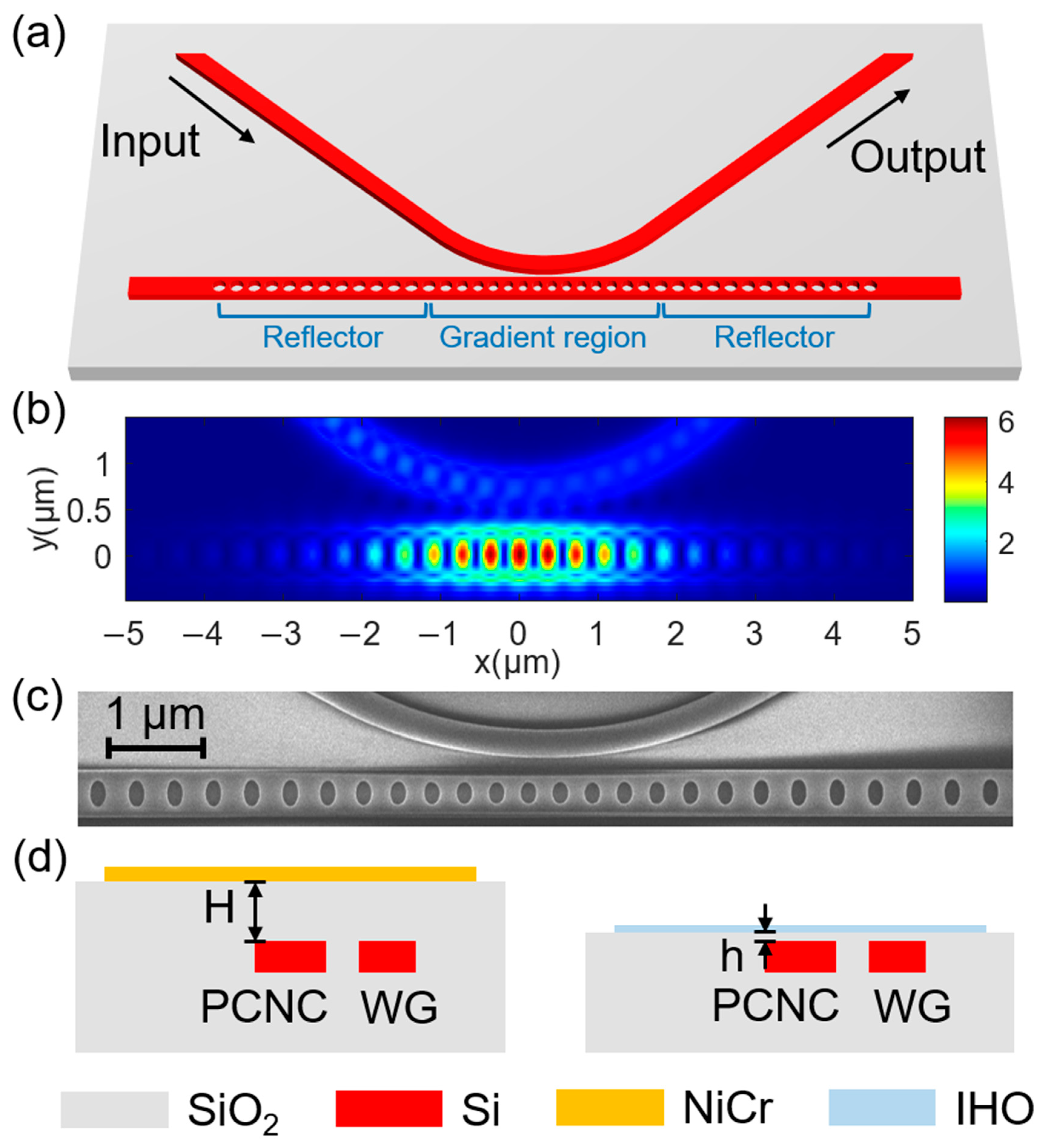
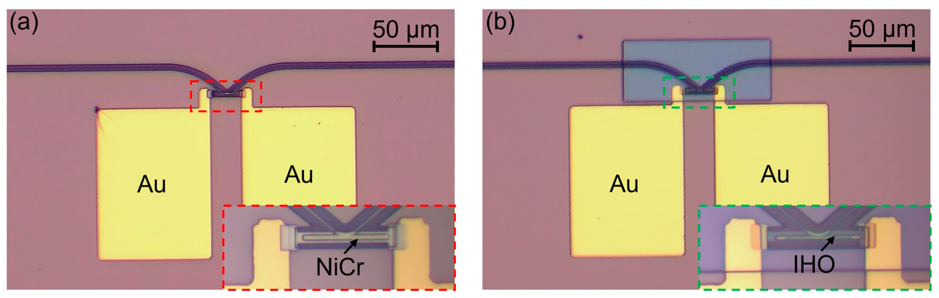
2. Methods
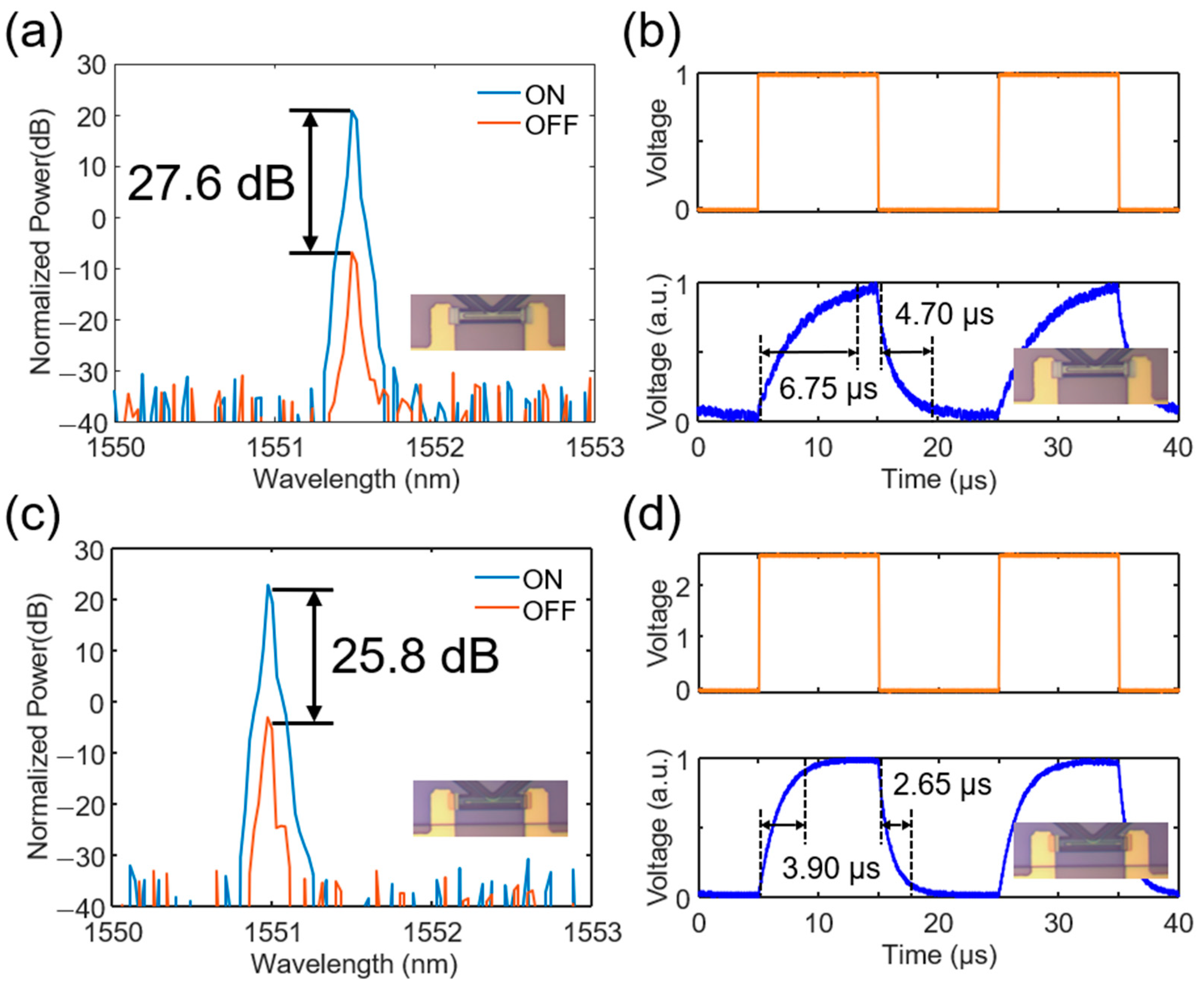
3. Results
4. Discussion
5. Conclusions
Author Contributions
Funding
Institutional Review Board Statement
Informed Consent Statement
Data Availability Statement
Conflicts of Interest
References
- Asghari, M.; Krishnamoorthy, A.V. Energy-efficient communication. Nat. Photonics 2011, 5, 268–270. [Google Scholar] [CrossRef]
- Hutchison, D.N.; Sun, J.; Doylend, J.K.; Kumar, R.; Heck, J.; Kim, W.; Phare, C.T.; Feshali, A.; Rong, H. High-resolution aliasing-free optical beam steering. Optica 2016, 3, 887–890. [Google Scholar] [CrossRef]
- Poulton, C.V.; Yaacobi, A.; Cole, D.B.; Byrd, M.J.; Raval, M.; Vermeulen, D.; Watts, M.R. Coherent solid-state LIDAR with silicon photonic optical phased arrays. Opt. Lett. 2017, 42, 4091–4094. [Google Scholar] [CrossRef] [PubMed]
- Poulton, C.V.; Byrd, M.J.; Russo, P.; Timurdogan, E.; Khandaker, M.; Vermeulen, D.; Watts, M.R. Long-Range LiDAR and Free-Space Data Communication with High-Performance Optical Phased Arrays. IEEE J. Sel. Top. Quantum Electron. 2019, 25, 7700108. [Google Scholar] [CrossRef]
- Wang, J.W.; Paesani, S.; Ding, Y.H.; Santagati, R.; Skrzypczyk, P.; Salavrakos, A.; Tura, J.; Augusiak, R.; Mancinska, L.; Bacco, D.; et al. Multidimensional quantum entanglement with large-scale integrated optics. Science 2018, 360, 285–291. [Google Scholar] [CrossRef] [PubMed]
- Qiang, X.; Zhou, X.; Wang, J.; Wilkes, C.M.; Loke, T.; O’Gara, S.; Kling, L.; Marshall, G.D.; Santagati, R.; Ralph, T.C.; et al. Large-scale silicon quantum photonics implementing arbitrary two-qubit processing. Nat. Photonics 2018, 12, 534–539. [Google Scholar] [CrossRef]
- Bao, J.; Fu, Z.; Pramanik, T.; Mao, J.; Chi, Y.; Cao, Y.; Zhai, C.; Mao, Y.; Dai, T.; Chen, X.; et al. Very-large-scale integrated quantum graph photonics. Nat. Photonics 2023, 17, 573–581. [Google Scholar] [CrossRef]
- Cheng, J.; Xie, Y.; Liu, Y.; Song, J.; Liu, X.; He, Z.; Zhang, W.; Han, X.; Zhou, H.; Zhou, K.; et al. Human emotion recognition with a microcomb-enabled integrated optical neural network. Nanophotonics 2023, 12, 3883–3894. [Google Scholar] [CrossRef]
- Zhang, J.; Wu, B.; Cheng, J.; Dong, J.; Zhang, X. Compact, efficient, and scalable nanobeam core for photonic matrix-vector multiplication. Optica 2024, 11, 190–196. [Google Scholar] [CrossRef]
- Zhang, S.; Zhou, H.; Wu, B.; Jiang, X.; Gao, D.; Xu, J.; Dong, J. Redundancy-free integrated optical convolver for optical neural networks based on arrayed waveguide grating. Nanophotonics 2024, 13, 19–28. [Google Scholar] [CrossRef]
- Liao, S.; Ding, Y.; Dong, J.; Wang, X.; Zhang, X. 125-GHz Microwave Signal Generation Employing an Integrated Pulse Shaper. J. Light. Technol. 2017, 35, 2741–2745. [Google Scholar] [CrossRef]
- Liu, S.; Wu, K.; Zhou, L.; Lu, L.; Zhang, B.; Zhou, G.; Chen, J. Microwave Pulse Generation with a Silicon Dual-Parallel Modulator. J. Light. Technol. 2020, 38, 2134–2143. [Google Scholar] [CrossRef]
- Sun, Y.; Wang, D.; Deng, C.; Lu, M.; Zhu, W.; Yun, B.; Hu, G.; Cui, Y. Frequency-selectable microwave generation based on on-chip switchable spectral shaping and wavelength-to-time mapping. Opt. Express 2023, 31, 3179–3186. [Google Scholar] [CrossRef] [PubMed]
- Espinola, R.L.; Tsai, M.C.; Yardley, J.T.; Osgood, R.M. Fast and low-power thermooptic switch on thin silicon-on-insulator. IEEE Photon. Technol. Lett. 2003, 15, 1366–1368. [Google Scholar] [CrossRef]
- Gan, S.; Cheng, C.; Zhan, Y.; Huang, B.; Gan, X.; Li, S.; Lin, S.; Li, X.; Zhao, J.; Chen, H.; et al. A highly efficient thermo-optic microring modulator assisted by graphene. Nanoscale 2015, 7, 20249–20255. [Google Scholar] [CrossRef] [PubMed]
- Yan, S.; Zhu, X.; Frandsen, L.H.; Xiao, S.; Mortensen, N.A.; Dong, J.; Ding, Y. Slow-light-enhanced energy efficiency for graphene microheaters on silicon photonic crystal waveguides. Nat. Commun. 2017, 8, 14411. [Google Scholar] [CrossRef]
- Liu, Y.J.; Wang, H.D.; Wang, S.; Wang, Y.J.; Wang, Y.Z.; Guo, Z.N.; Xiao, S.M.; Yao, Y.; Song, Q.H.; Zhang, H.; et al. Highly Efficient Silicon Photonic Microheater Based on Black Arsenic-Phosphorus. Adv. Opt. Mater. 2020, 8, 1901526. [Google Scholar] [CrossRef]
- Cheng, Z.; Cao, R.; Guo, J.; Yao, Y.; Wei, K.; Gao, S.; Wang, Y.; Dong, J.; Zhang, H. Phosphorene-assisted silicon photonic modulator with fast response time. Nanophotonics 2020, 9, 1973–1979. [Google Scholar] [CrossRef]
- Parra, J.; Hurtado, J.; Griol, A.; Sanchis, P. Ultra-low loss hybrid ITO/Si thermo-optic phase shifter with optimized power consumption. Opt. Express 2020, 28, 9393–9404. [Google Scholar] [CrossRef]
- Tong, W.; Yang, E.; Pang, Y.; Yang, H.; Qian, X.; Yang, R.; Hu, B.; Dong, J.; Zhang, X. An Efficient, Fast-Responding, Low-Loss Thermo-Optic Phase Shifter Based on a Hydrogen-Doped Indium Oxide Microheater. Laser Photon. Rev. 2023, 17, 2201032. [Google Scholar] [CrossRef]
- Watts, M.R.; Sun, J.; DeRose, C.; Trotter, D.C.; Young, R.W.; Nielson, G.N. Adiabatic thermo-optic Mach-Zehnder switch. Opt. Lett. 2013, 38, 733–735. [Google Scholar] [CrossRef] [PubMed]
- Tong, W.Y.; Wei, Y.X.; Zhou, H.L.; Dong, J.J.; Zhang, X.L. The Design of a Low-Loss, Fast-Response, Metal Thermo-Optic Phase Shifter Based on Coupled-Mode Theory. Photonics 2022, 9, 447. [Google Scholar] [CrossRef]
- Wei, Y.X.; Cheng, J.W.; Wang, Y.L.; Zhou, H.L.; Dong, J.J.; Huang, D.M.; Li, F.; Li, M.; Wai, P.K.A.; Zhang, X.L. Strategy for Low-Loss Optical Devices When Using High-Loss Materials. Adv. Photonics Res. 2022, 3, 2200120. [Google Scholar] [CrossRef]
- Zhong, C.; Ma, H.; Sun, C.; Wei, M.; Ye, Y.; Tang, B.; Zhang, P.; Liu, R.; Li, J.; Li, L.; et al. Fast thermo-optical modulators with doped-silicon heaters operating at 2 μm. Opt. Express 2021, 29, 23508–23516. [Google Scholar] [CrossRef]
- Oz, D.; Suleymanov, N.; Minkovich, B.; Kostianovskii, V.; Gantz, L.; Polyushkin, D.; Mueller, T.; Goykhman, I. Optically Transparent and Thermally Efficient 2D MoS2 Heaters Integrated with Silicon Microring Resonators. ACS Photonics 2023, 10, 1783–1794. [Google Scholar] [CrossRef]
- Chung, S.; Nakai, M.; Hashemi, H. Low-power thermo-optic silicon modulator for large-scale photonic integrated systems. Opt. Express 2019, 27, 13430–13459. [Google Scholar] [CrossRef] [PubMed]
- Qiu, H.; Liu, Y.; Luan, C.; Kong, D.; Guan, X.; Ding, Y.; Hu, H. Energy-efficient thermo-optic silicon phase shifter with well-balanced overall performance. Opt. Lett. 2020, 45, 4806–4809. [Google Scholar] [CrossRef]
- Nejadriahi, H.; Pappert, S.; Fainman, Y.; Yu, P. Efficient and compact thermo-optic phase shifter in silicon-rich silicon nitride. Opt. Lett. 2021, 46, 4646–4649. [Google Scholar] [CrossRef] [PubMed]
- Xu, Z.; Qiu, C.; Yang, Y.; Zhu, Q.; Jiang, X.; Zhang, Y.; Gao, W.; Su, Y. Ultra-compact tunable silicon nanobeam cavity with an energy-efficient graphene micro-heater. Opt. Express 2017, 25, 19479–19486. [Google Scholar] [CrossRef]
- Zhou, H.; Qiu, C.; Jiang, X.; Zhu, Q.; He, Y.; Zhang, Y.; Su, Y.; Soref, R. Compact, submilliwatt, 2 × 2 silicon thermo-optic switch based on photonic crystal nanobeam cavities. Photonics Res. 2017, 5, 108–112. [Google Scholar] [CrossRef]


| Structure | Method | Ref | Power [mW] | Efficiency [nm/mW] | ER [dB] | Response Time [μs] | Year |
|---|---|---|---|---|---|---|---|
| MZI | PhCW a + graphene | [16] | 3.99 | 1.07 | ~8 | 0.750/0.525 | 2017 |
| strip WG + IHO | [20] | 9.6 | 0.0472 | ~20 | 0.970/0.980 | 2023 | |
| adiabatic bend + doped silicon | [21] | 12.7 | \ | ~25 | 1.2/2.4 | 2013 | |
| MRR | rib WG + graphene | [15] | 28 | ~0.104 | 7 | 0.700/0.800 | 2015 |
| rib WG + doped silicon | [24] | 3.33 | 0.1 | ~8 | 3.56/3.70 | 2021 | |
| strip WG + MoS2 | [25] | 7.5 | 0.1 | ~25 | 26/24 | 2023 | |
| PCNC | strip WG + graphene | [29] | \ | 1.5 | 8 | 1.11/1.47 | 2017 |
| strip WG + Ti | [30] | 0.16 | 1.23 | 15 | 3.1/4.5 | 2017 | |
| strip WG + TiCr | this work | 5.60 | 0.907 | 27.6 | 6.75/4.70 | ||
| strip WG + IHO | this work | 2.86 | 1.326 | 25.8 | 3.90/2.65 |
Disclaimer/Publisher’s Note: The statements, opinions and data contained in all publications are solely those of the individual author(s) and contributor(s) and not of MDPI and/or the editor(s). MDPI and/or the editor(s) disclaim responsibility for any injury to people or property resulting from any ideas, methods, instructions or products referred to in the content. |
© 2024 by the authors. Licensee MDPI, Basel, Switzerland. This article is an open access article distributed under the terms and conditions of the Creative Commons Attribution (CC BY) license (https://creativecommons.org/licenses/by/4.0/).
Share and Cite
Tong, W.; Li, S.; Zhang, J.; Dong, J.; Hu, B.; Zhang, X. Thermo-Optic Switch with High Tuning Efficiency Based on Nanobeam Cavity and Hydrogen-Doped Indium Oxide Microheater. Photonics 2024, 11, 738. https://doi.org/10.3390/photonics11080738
Tong W, Li S, Zhang J, Dong J, Hu B, Zhang X. Thermo-Optic Switch with High Tuning Efficiency Based on Nanobeam Cavity and Hydrogen-Doped Indium Oxide Microheater. Photonics. 2024; 11(8):738. https://doi.org/10.3390/photonics11080738
Chicago/Turabian StyleTong, Weiyu, Shangjing Li, Jiahui Zhang, Jianji Dong, Bin Hu, and Xinliang Zhang. 2024. "Thermo-Optic Switch with High Tuning Efficiency Based on Nanobeam Cavity and Hydrogen-Doped Indium Oxide Microheater" Photonics 11, no. 8: 738. https://doi.org/10.3390/photonics11080738