Abstract
In this study, an ultra-wideband absorber spanning from UV-B to middle-IR was designed and analyzed using a novel structure. The multilayer metamaterial, arranged from bottom to top, consisted of an Al metal layer, a lower SiO2 layer, a graphite layer, another SiO2 layer, a thin Ti layer, and a top SiO2 layer. The top layer of SiO2 had a 200 nm square cavity etched out, and then a square Ti nanopillar and a square Ti hollow outside a Ti nanopillar were embedded. This specific arrangement was chosen to maximize the absorption properties across a broad spectrum. The absorption spectrum of the designed absorber was thoroughly analyzed using the commercial finite element analysis software COMSOL Multiphysics® (version 6.0). This analysis confirmed that the combination of these various components achieved perfect absorption and an ultra-wideband response. The synergistic interaction between the layers and the nanopillars structure contributed significantly to the absorber’s efficiency, making it a promising candidate for applications requiring broad-spectrum absorption. The comprehensive analyses of the parameters for different structures demonstrated that the effects of guided-mode resonance, coupling resonance, optical impedance matching, and propagating surface plasmon resonance existed in the investigated structure. The optimal model, determined through analyses using COMSOL Multiphysics®, showed that the broadband absorption in the range of 270 to 3600 nm, spanning from UV-B to middle-IR, exceeded 90.0%. The average absorption rate within this range was 0.967, with the highest reaching a near-perfect absorptivity of 99.9%. We also compared three absorption spectra in this study: the t1–t6 flat structure, the t1–t5 flat structure with t6 featuring a square cavity, and the structure proposed in this study. This demonstrates that a square nanopillar and a square hollow embedded in a square cavity can enhance the absorptive properties of the absorber.
1. Introduction
Electromagnetic absorbers are devices designed to effectively capture and convert incident electromagnetic radiation within specific frequency bands into usable energy. These absorbers are broadly categorized into two types: wideband absorbers and resonant absorbers. The resonant absorbers interact with incident radiation at specific or multiple resonance wavelengths (frequencies) [1,2,3]. In contrast, the wideband absorbers utilize a two-dimensional periodic structure to transition the dielectric constant from free space to the absorber, relying on materials with high inherent loss [4,5,6]. Metamaterials are artificial materials that exhibit unique properties, such as electromagnetic bandgaps [7], near-zero indices [8], and negative refractive indices [9]. One of their most promising characteristics is that they can be used to process the perfect absorption. Metamaterial absorbers typically consist of a resonant structure composed of one or more dielectric and metal layers atop a metallic ground plane. These absorbers allow waves at resonant frequencies to enter but prevent them from passing through, resulting in superior absorption.
Multilayer optical absorbers were typically designed using alternating layers of metals and dielectric materials. Although graphite has been used in designing optical absorbers before, there has been limited use of graphite directly replacing metal layers [10,11,12]. When designing an optical absorber, graphite can partially replace the metal layer due to its ability to absorb light across a wide spectrum. However, it cannot fully replace the metal layer for several reasons. Metals typically have higher optical absorption coefficients across a broader range of wavelengths compared to graphite. This means metals can absorb more incident light efficiently, which is crucial for many optical applications. Metals are excellent electrical conductors, which is often necessary in applications where the absorber needs to dissipate heat or maintain specific electrical properties. Graphite, while a good conductor, may not match the conductivity of metals in all scenarios. A primary innovation of this study is replacing metallic layers with graphite in one of these layers. The advantages of using graphite instead of metal layers in designing light absorbers are as follows:
- Graphite possesses excellent light absorption characteristics, particularly within the visible and near-infrared spectra. Therefore, employing graphite as a light absorber can effectively enhance energy conversion efficiency.
- Graphite is relatively cheaper than metals and is easier to process and manufacture. This can significantly reduce design costs, especially during large-scale production.
- Graphite is typically lighter than metals, allowing for the creation of lightweight structures in optical component designs. Moreover, graphite can enhance flexibility in shaping and structuring, thereby better accommodating various application needs.
- Graphite exhibits excellent corrosion resistance and higher temperature tolerance than most metals, ensuring stable performance in diverse environmental conditions.
In the past, various methods have been employed to enhance the maximum absorptivity and broaden the bandwidth of designed absorbers with absorptivity exceeding 90% [13,14]. For instance, Huang et al. investigated a highly efficient absorber capable of ultra-broadband absorption spanning from ultraviolet (UV) to near infrared (NIR), achieved using a metamaterial perfect absorber composed of refractory materials [15]. Tharwat et al. utilized a metal–dielectric–metal functional stack with a circular cap to develop a plasmonic metamaterial absorber achieving an absorptivity above 90% within the wavelength range of approximately 420 to 1650 nm [16]. Similarly, Hakim et al. explored an ultrathin concentric hexagonal ring resonator metamaterial absorber. This absorber demonstrated an absorptivity exceeding 90% across the 380 to 2500 nm range, with an impressive average absorptivity of 96.64% [17]. Sun et al. investigated a broadband, near-perfect metamaterial solar absorber composed of a TiN reflector layer, an insulating SiO2 layer, and a TiN ring array. This absorber achieved an impressive average absorptivity of 97.6% over the wavelength range of 300–2500 nm [18]. Similarly, Peng et al. designed a multilayer, planar metamaterial absorber featuring a MgF2 layer as the top anti-reflection layer. Their absorber exhibited an absorptivity of 90% and an average absorptivity of 97.0% across an ultra-broadband range spanning from 410 to approximately 2300 nm [19]. Despite their high performance in specific wavelength ranges, their absorptive bandwidth was not consistently maintained above 90.0% throughout the broader UV-B to middle-IR spectrum. Further research and developments are necessary to enhance the broadband absorptivity of these metamaterial absorbers to cover this extended range more effectively.
In essence, utilizing graphite instead of metal layers in designing light absorbers not only improves performance and efficiency but also reduces costs while enhancing design flexibility and durability. When designing a solar absorber, incorporating a cavity structure at the top layer is aimed at increasing the light absorption surface area, thereby enhancing energy conversion efficiency. The cavity structure serves to effectively expand the absorber’s active surface area and lengthen the optical path for improved light absorption, particularly for parallel incident rays. This design approach facilitates greater absorption and conversion of solar energy into heat or electricity [12,20,21,22]. The second innovative feature of this study involved excavating square matrix cavities in the top oxide (SiO2) layer and placing a metal (Ti) square nanopillar and a metal (Ti) square hollow inside each cavity. When designing a solar light absorber, excavate square cavities in the top oxide layer and place metal square nanopillars and square hollows inside. The matrix-like structure of the investigated absorber is shown in Figure 1, and this design offers several advantages:
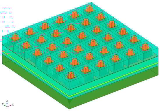
Figure 1.
The matrix-like structure of the investigated absorber.
- Metal nanostructures can enhance light absorption through surface plasmon resonance (SPR) and the geometric design of square nanopillars and hollows can be tailored to maximize absorption at specific wavelengths.
- Metal nanostructures effectively reduce light reflection, thereby increasing energy conversion efficiency. Square nanopillars and hollows can guide and capture multiple reflections of light, ensuring more light is absorbed and utilized.
- Metal nanostructures typically provide broad-spectrum light absorption capabilities, effectively harnessing solar energy across the broadband wavelength ranges.
- A coupling resonance effect occurs when resonant structures (such as nanopillars and hollows) interact closely, influencing each other’s resonance characteristics to create new resonance modes [6]. Placing square nanopillars and hollows within square cavities leverages the principles of SPR and coupled resonances to maximize light absorption and minimize reflection.
This study focused on replacing traditional metallic layers with graphite material, aiming to reduce material costs and minimize optical losses effectively. In device design, we utilized square matrix cavities on the top SiO2 layer, each housing metal square nanopillars and square hollow structures. This design not only exhibited high symmetry and regularity in structure but also efficiently captured and absorbed photon energy across a broad spectrum. The comprehensive analyses of the parameters of the designed absorber would demonstrate that the effects of guided-mode resonance, coupling resonance, optical impedance matching, and propagating surface plasmon resonance coexist in the investigated structure. The absorber demonstrated exceptional optical performance, achieving over 90% absorption efficiency across wavelengths from 270 nm to 3600 nm. This capability extended from absorbing ultraviolet B (UV-B) radiation (280 to 320 nm) to encompassing the entire NIR range, which includes IR-A (0.78 to 1.4 μm), IR-B (1.4 to 3 μm), and the middle-infrared (middle-IR) wavelengths (3 to 50 μm). Moreover, the use of graphite material offered additional advantages such as lower reflectivity and broader optical bandgaps, positively impacting absorber design and performance. This research not only expands the application range of ultra-wideband absorbers but also opens new technological pathways for future optoelectronic and optical device designs.
2. Structure of the Investigated Bidirectional Switching Functionality Absorber
Designing an optical absorber capable of operating from UV-B (270 nm) to middle-IR (3600 nm) wavelengths necessitated meticulous and precise construction to effectively capture light across this extensive spectrum. The finite element software COMSOL Multiphysics® (version 6.0) was used as the tool to conduct the simulation processes. The structure utilized in this research is illustrated in Figure 2a, with detailed parameters for each layer provided in Figure 2b. The dielectric layers comprised solely SiO2, while the chosen conducting layers were Ti and graphite. These materials were selected for their established deposition processes and cost-effectiveness, and are widely used in designing optical absorbers with high absorption efficiency across a broad spectrum. The absorber structure featured alternating layers of conductive materials and SiO2, arranged as Al (t1)/SiO2 (t2)/graphite (t3)/SiO2 (t4)/Ti (t5)/SiO2 (t6)/Ti (t7) from bottom to top. The thicknesses of each layer, in sequence from bottom to top, were 300 nm/80 nm/40 nm/140 nm/7 nm/255 nm/205 nm. However, other parameters were optimized iteratively by systematically adjusting t1 to t8 and w1, while keeping the original parameters shown in Figure 2b unchanged, in order to find their optimal values. It is noteworthy that the t1 to t7 layers formed continuous planes, primarily adjusting the width of the square cavity in the top layer to regulate the spaces between adjacent widths of w2 to w5 as shown in Figure 2c.
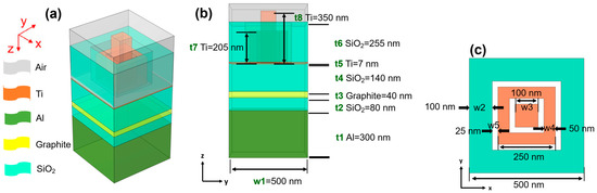
Figure 2.
(a) Structure, (b) side view with parameters, and (c) top view with parameters.
The t1 Al layer primarily served as the substrate layer, thus its thickness was fixed at 300 nm and would not undergo thickness variation analysis. After careful simulations, the widths of w1, w2, w3, w4, and w5 were measured to be 500 nm, 100 nm, 100 nm, 50 nm, and 25 nm, respectively. The optimization process began with identifying appropriate parameters, followed by refining the search based on these findings. Parameters t1 to t8 were fixed according to the values shown in Figure 2b, while the optimal design parameter for t2 was subsequently determined. After determining the optimal value for t2, the design parameters for t1 and t2 were fixed, and the search proceeded sequentially to identify other optimal design parameters. The absorber under investigation had a mesh structure with the following specifications: 8707 grid nodes, featuring a minimum grid length of 0.8 nm and a maximum of 1.6 nm. The mesh consisted of 48,775 tetrahedral elements and 9932 triangular elements, complemented by 64 endpoint elements and 838 edge finite elements. The average element quality was 0.6304, with a minimum of 0.1363. The total grid area was 2.442 × 10⁸ nm2 and the element to volume ratio was 6.141 × 10⁻⁵ ensuring the accuracy and reliability of the simulation results.
3. Results and Discussion
When the thickness of the t2 SiO2 layer varies from 82 to 90 nm, Figure 3a illustrates three peaks where absorptivity suddenly drops. To comprehend the underlying reasons for this phenomenon, an analysis of absorptivity distribution across wavelengths ranging from 270 to 3800 nm, along with variations in t2 thickness from 70 to 90 nm, is necessary. Figure 3b demonstrates how changes in t2 thickness and wavelength affect the absorptivity of the investigated absorber. It reveals that for the t2 SiO2 layer, the range of high absorptivity extends approximately from 270 to 3600 nm as the thickness varies from 70 to 90 nm. However, Figure 3b also clearly indicates that when the t2 SiO2 layer thickness is less than 78 nm or greater than 86 nm, there are resonant peaks at specific wavelengths where absorptivity abruptly decreases. While a thickness of 80 nm achieves higher absorptivity, this tolerance for thickness variation is very narrow. Deviations slightly beyond 78 nm lead to resonant peak issues and sudden drops in absorptivity. Therefore, this thickness is impractical. To facilitate manufacturing, we adjusted the thickness to 82 nm, where we observed that the t2 SiO2 layer maintains consistent absorption spectrum performance compared to 80 nm, with no significant variations. This adjustment aims to provide greater tolerance in thickness variation while maintaining high absorptivity performance of the t2 SiO2 layer.
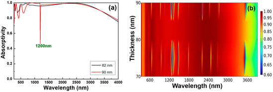
Figure 3.
Effect of the thickness of the t2 SiO2 layer on the (a) absorption spectrum and (b) the absorptivity of the absorber with the investigated structure.
Figure 4a shows that when the thickness of the t3 graphite layer varies from 38 to 45 nm, there are several peaks where absorptivity suddenly drops. To understand the reasons behind this phenomenon, absorptivity versus wavelength and thickness t3 distribution maps are needed. Figure 4b illustrates how variations in t3 thickness and wavelength impact the absorptivity of the absorber under investigation. It reveals that for graphite at different thicknesses such as 50 or 38 nm, the range of high absorptivity extends from approximately 270 nm to about 3600 nm. Additionally, Figure 4b indicates that at certain t3 thicknesses and wavelengths, there are abrupt drops in overall absorptivity. The causes behind these sudden drops in absorptivity observed in Figure 3b and Figure 4b will be discussed later. Although a thickness of 50 nm achieves high absorptivity, this thickness allows for very small tolerances in thickness variations. Deviating slightly beyond 52 nm or below 49 nm results in resonant peak issues with abrupt drops in absorptivity. Therefore, this thickness is not practical. To facilitate easier manufacturing, we adjusted the thickness of the t3 graphite layer to 38 nm, where similar resonant peak issues occur if the thickness of the t3 graphite layer exceeds 42 nm or falls below 35 nm. This adjustment aims to balance high absorptivity with practical manufacturing constraints, providing a more forgiving tolerance in thickness variations while maintaining high absorptivity performance.
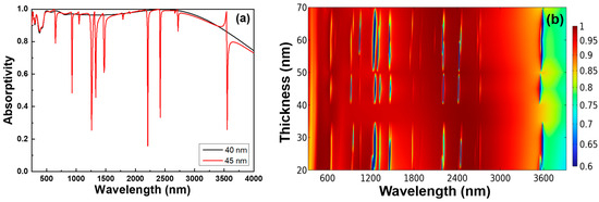
Figure 4.
Effect of the thickness of the t3 graphite layer on the (a) absorption spectrum and (b) the absorptivity of the absorber with the investigated structure.
Guided-mode resonance (GMR) is a phenomenon observed in optical systems, particularly in gratings or thin film structures. This effect occurs when optical waves are coupled into and resonate within a waveguide under specific conditions, leading to enhanced absorption or reflection of light propagating through the waveguide [23,24]. The fundamental principles of GMR include the following:
- GMR typically occurs in structures containing gratings or multilayer films. The periodicity and thickness of these structures need to be carefully designed to allow resonance of light at specific wavelengths.
- When light of a particular wavelength is incident at the correct angle onto the structure, it interacts with the modes within the structure. The incident angle and wavelength must satisfy resonance conditions, determined by the physical dimensions and material properties of the structure.
- Under resonance conditions, the incident light wave couples with the guided modes inside the structure and leads to the propagation of light waves within the waveguide in specific modes. This coupling effect is influenced by the periodic structure of the grating or the refractive index distribution of the thin film.
- Light waves inside the waveguide resonate in specific modes determined by the geometric shape and material properties of the waveguide. Resonance modes strongly depend on the wavelength and angle of incident light.
- Under resonance conditions, light waves are locally amplified within the waveguide and undergo multiple reflections. This results in strong reflection or transmission of light at certain wavelengths, forming distinct resonance peaks or dips.
- GMR causes significant changes in the optical properties of the structure, and at resonance wavelengths, the structure may exhibit high reflectance or high transmittance.
Understanding these principles is crucial for designing optical devices that leverage GMR for enhanced light manipulation and control. When designing a broadband absorber, employing the film resonance effect significantly enhances the absorption bandwidth from ultraviolet to infrared regions [25,26]. This enhancement is achieved through several mechanisms, including interference effects in multilayer structures, localized surface plasmon resonance, the coupling of multiple resonance modes, optimized light-trapping structure design, and careful selection and adjustment of material layers. Similarly, these factors can cause a broadband absorber design to exhibit sharp increases in reflectance and decreases in absorbance at certain thicknesses and wavelengths.
Figure 5 analyzes the effects of the analysis wavelength and the thickness of the t4 SiO2 layer on the absorption spectrum, as shown in Figure 5a, and on the absorptivity of the absorber, as shown in Figure 5b. Figure 5a clearly demonstrates that when the thickness of the t4 SiO2 layer is adjusted from the initial 140 to 125 nm, the absorptivity in the short-wavelength range of 270–530 nm cannot be increased to above 90%. Moreover, there are several noticeable resonance peaks where the absorptivity significantly decreases. From Figure 5b, which illustrates the absorptivity as a function of both the thickness of the t4 SiO2 layer and the wavelength, it is evident that when the thickness of the t4 SiO2 layer is less than 175 nm, the absorptivity in the short-wavelength range of 270–530 nm is notably below 90%. Additionally, for wavelengths exceeding 3000 nm, the long-wavelength absorption bandwidth clearly increases with the increase in layer thickness. Therefore, the thickness of the t4 SiO2 layer is set to 180 nm. As shown in Figure 5a, this adjustment results in the absorptivity in the short-wavelength range of 270–530 nm being increased to above 90%. Figure 5 also clearly demonstrates that selecting an appropriate thickness can prevent the designed absorber from experiencing significant decreases in absorptivity at the resonance peaks caused by the GMR effect. By choosing a suitable thickness, the GMR effect can instead enhance the absorptivity and expand the absorption bandwidth, making the absorber more efficient.
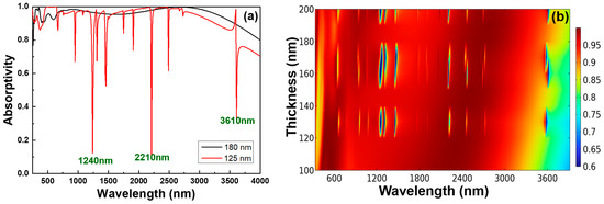
Figure 5.
Effect of the thickness of the t4 SiO2 layer on the (a) absorption spectrum and (b) the absorptivity of the absorber with the investigated structure.
After analyzing the thicknesses of the t5 Ti layer and t6 SiO2 layer, and the height of the t7 square hollow, it was determined that values of 7 nm for t5, 255 nm for t6, and 205 nm for t7, represented the optimal configurations where the absorption spectrum remained largely unchanged. Therefore, no further adjustments were made to these thicknesses or heights. Figure 6a clearly demonstrates that when the height of the t8 square nanopillar decreases from 350 to 290 nm, there are two resonant absorption peaks with absorptivity falling below 90% within the 270–700 nm range. This indicates a significant reduction in absorption efficiency at these resonant peaks. From Figure 6b, which shows the absorptivity distribution relative to both the height of the t8 square nanopillar and the analysis wavelength, it is evident that at smaller nanopillar heights, such as below 320 nm, the absorptivity significantly decreases within the 270–700 nm range. This suggests that the initially set height of 290 nm is not optimal for the t8 square nanopillar. When we adjusted the height of the t8 square nanopillar from 350 to 340 nm, we could clearly avoid a sudden drop in absorptivity around the 3500 nm range. These results further prove that by choosing a suitable thickness, the GMR effect can instead enhance the absorptivity and expand the absorption bandwidth, making the absorber more efficient.
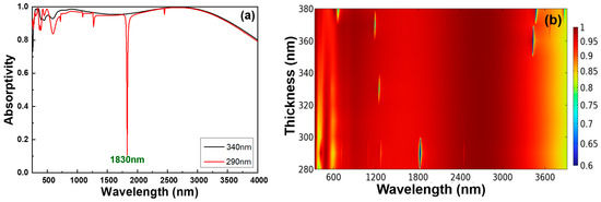
Figure 6.
Effect of the height of the t8 square nanopillar on the (a) absorption spectrum and (b) the absorptivity of the absorber with the investigated structure.
The analysis results highlight the critical role of each layer’s thickness and the height of the square nanopillar (and the height of the square hollow, though further analysis of this factor is not shown here) in determining the absorptivity and efficiency of the absorber. For example, the reduction in absorptivity at specific heights can be attributed to the mismatch between the nanopillar height and the incident wavelength, leading to destructive interference and diminished absorption. By carefully adjusting the height to 340 nm, the resonance conditions shift, avoiding detrimental resonant peaks and enhancing overall absorptivity. These findings suggest that the absorber’s performance can be significantly improved through meticulous tuning of the structural parameters. Additionally, investigating the impact of other geometrical factors, such as the different thicknesses of different layer materials and the different heights of the nanopillars, could further enhance the absorber’s efficiency. This comprehensive approach could pave the way for the development of highly efficient, robust, and versatile absorbers for a wide range of optical applications.
In conclusion, the absorptivity of the optical absorber under investigation is significantly influenced by the structural design, including the thickness of each layer, as well as the heights of the square nanopillars and square hollows. By carefully adjusting these parameters, it becomes possible to effectively control absorptivity across a wide spectrum ranging from 270 to 3600 nm. Specifically, the height of the t8 square nanopillar was optimized within a range of 280 to 380 nm. After thorough optimization, a height of 340 nm was determined to be the optimal t8 value. This comprehensive optimization process enhances the absorber’s performance and applicability in various optical applications. Table 1 presents a comparison between the original design and the modified parameters. This absorption spectra for the original design and the modified parameters are compared in Figure 7, where the black line is the result for using the parameters of the original design and the red line is that for using the modified parameters. Notably, after optimizing the structural parameters in our research design, our metamaterial structure featuring a square nanopillar and a square hollow embedded within the square cavity of the top layer consistently achieves absorptivity exceeding 0.9 across a broad spectrum from 270 to 3600 nm. Specifically, we have addressed the previous issue where absorptivity was below 0.9 at 420 nm, achieving significant improvement. Moreover, the average absorptivity across the range of 270 to 3600 nm has increased from 0.955 to 0.967.

Table 1.
A comparison between the original design and the modified parameters.
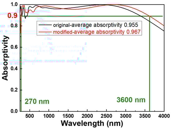
Figure 7.
Comparison of the absorptivity spectra for the originally designed parameters and the modified parameters.
To demonstrate the main factor behind achieving an ultra-wideband absorber spanning from UV-B to mid-IR wavelengths in our study, the structures were simulated under different configurations. Figure 8a illustrates the configuration without the square nanopillar and the square hollow, while Figure 8b depicts the absorber with the six continuous planes, which means the absorber without both the square nanopillar and the square hollow, and the square cavity in the top layer of the multilayer metamaterials. The simulation results of the two structures in Figure 8 are compared with the simulation results of the structure in Figure 2, which utilizes the modified parameters from Table 1. The comparative results of these simulation absorption spectra of three different structures are presented in Figure 9. The absorption spectra of the two structures in Figure 8 do not exhibit ultra-broadband absorption characteristics, and there are numerous sharp drops in absorptivity within both spectra. This indicates that the GMR effect is indeed present in the original multilayer thin-film structure and also in the structure with a square cavity etched into the multilayer thin films. However, when square cavities are arranged in a matrix and each cavity is embedded with a square nanopillar and a square hollow, the GMR effect is neutralized. In addition to the GMR effect, Figure 9 also shows that the structure with six continuous planes exhibits a significantly reduced bandwidth. When the structure lacks a square nanopillar and square hollow embedded within the square cavity, there is a prominent peak in absorptivity drop. Conversely, incorporating a structure with a square nanopillar and square hollow enhances absorptivity and expands the bandwidth. This demonstrates that a square nanopillar and square hollow can induce coupling resonance effects within the square cavity. These coupling resonance effects notably enhance absorber absorptivity and broaden the absorption bandwidth. Consequently, the designed absorber achieves ultra-broadband and high absorptivity characteristics.
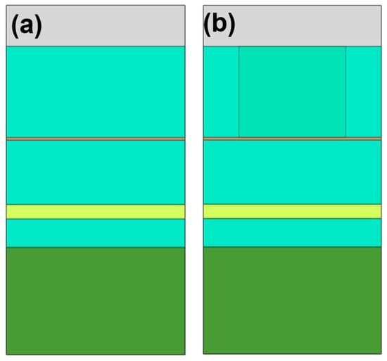
Figure 8.
The investigated absorber (a) without a square nanopillar and a square hollow and (b) without a square nanopillar and a square hollow and without a square cavity in the top layer of multilayer metamaterials.
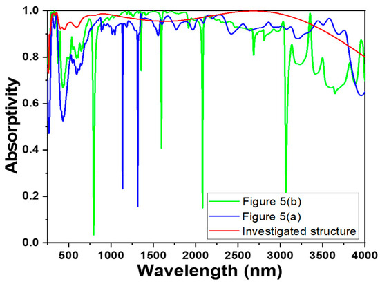
Figure 9.
The absorption spectra for different absorbers, including the investigated absorber, the absorber with the six continuous planes, and the investigated absorber without a square nanopillar and a square hollow.
The relationship between the Z parameters and free space impedance S can be determined from the effective medium theory, which is expressed as follows [27,28]:
In the two formulas, k, d, and n are the wave vector, the thickness of the designed absorber, and the refractive index of the utilized material, respectively. S11, S12, S21, and S22 represent the S parameters, with the reflectivity R defined as S11. When the utilized metal substrate exceeds the skin depth of the incident light, the transmittance ratio can be defined as T = S12 = 0. The free space impedance of the designed absorber is given by:
A designed absorber can achieve maximum absorptivity when its impedance matches that of free space, or when Z = Z0. As illustrated in Figure 10, for the designed absorber depicted in Figure 2, using the modified parameters outlined in Table 1, the imaginary part of the impedance is close to zero, and the real part is near one. This impedance matching ensures that the designed absorber exhibits optimal absorption performance, closely aligning with perfect absorptivity over a wide bandwidth. This optimal performance is critical for applications requiring efficient energy capture across a broad range of frequencies. The near-zero imaginary part indicates minimal energy loss, while the real part being close to one signifies excellent impedance matching. Consequently, the absorber efficiently converts incident electromagnetic waves into heat or another form of energy without significant reflection.
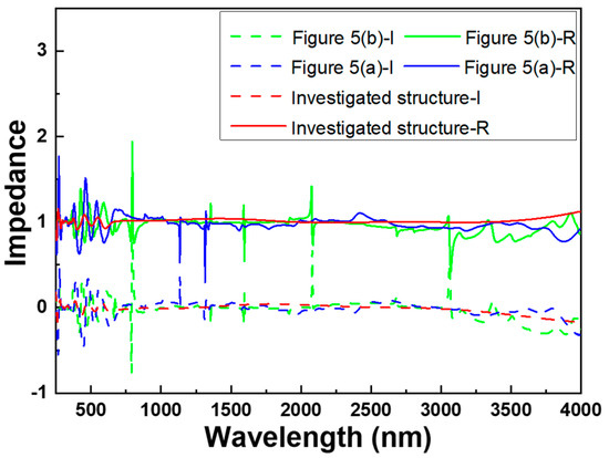
Figure 10.
Optical impendence for different absorbers, including the investigated absorber, the absorber with the six continuous planes, and the investigated absorber without a square nanopillar and a square hollow.
The results in Figure 10 also indicate that when the structures shown in Figure 5a,b are used for simulations, within the wavelength range of approximately 400–750 nm, the real part of the impedance for both structures deviates from one, and the imaginary part deviates from zero. This deviation is the primary reason for the lower absorptivity of the structures in Figure 5a,b within this wavelength range. Specifically, when the structure in Figure 5a is simulated, the results in Figure 10 show two peaks where the real part of the impedance deviates from one. These peak wavelengths correspond to the wavelengths where there are sharp drops in absorptivity in Figure 9 for the simulation results of the Figure 5a structure. Similarly, when the structure in Figure 5b is simulated, the results in Figure 10 also show peaks where the real part of the impedance deviates from one and the imaginary part deviates from zero. These wavelengths correspond to the wavelengths where there are sharp drops in absorptivity in Figure 9 for the simulation results of the Figure 5b structure. Therefore, it is evident that the GMR effect, which causes a decrease in absorptivity, is significantly related to the optical impedance. The mismatched impedance disrupts the absorption efficiency, leading to suboptimal performance in the 400–750 nm range. This emphasizes the importance of achieving impedance matching to ensure high absorptivity across a broad spectrum.
LSPR (localized surface plasmon resonance) refers to a resonance phenomenon occurring on the surface of metallic nanostructures when interacting with light waves. This phenomenon leads to the localization of optical energy near the surface of the metal structures. LSPR can result in high absorption rates within specific wavelength ranges and also affect the penetration depth of light, especially in interactions involving layered structures of metals and dielectrics. PSPR (propagating surface plasmon resonance) is a similar effect to LSPR but involves multi-layered structures or specific geometric shapes that can more effectively enhance the localized optical field intensity. This effect is particularly pronounced in complex structures alternating between multiple layers of metals and dielectrics, potentially leading to deeper light absorption depths as photons are efficiently concentrated and absorbed within such configurations. SPR, LSPR, and PSPR are all phenomena involving the interaction of light with metallic nanostructures, but they exhibit important differences. SPR (surface plasmon resonance) is a collective oscillation where free electrons near the surface of a metal oscillate. SPR occurs when the optical constants of light and a metal surface are closely matched, leading to shallow absorption depths typically ranging from tens to hundreds of nanometers. LSPR involves metallic nanoparticles (NPs) interacting with light, where resonance depends on the NP sizes and shapes matching the incident light wavelength. PSPR occurs when the geometric characteristics of metallic nanostructures align with incident light, resulting in absorption depths falling between those of SPR and LSPR. However, LSPR usually results in absorption depths from hundreds to thousands of nanometers, whereas PSPR’s absorption depth falls between SPR and LSPR.
An ultra-wideband optical absorber refers to a material or structure designed to absorb light across a broad spectrum within the UV, visible, and IR ranges of wavelengths. Figure 9 clearly provides insights into the analysis results of the electric field, as shown in Figure 11a, and magnetic field, as shown in Figure 11b, processes at wavelengths of 270, 460, 520, 900, and 2680 nm. As shown in Figure 11a,b, the high absorption range extends from the top square nanopillar, square hollow, and square cavity structures all the way to the t2 SiO2 layer. The effect of the Fabry–Perot cavity, typically present in a multilayer absorber between two metallic layers, does not manifest in the energy distributions of the electric or magnetic fields at these five resonance wavelengths. In cases where light absorption depths reach approximately 1000 nanometers, it is typically more associated with PSPR. PSPR involves the propagation of surface plasmons on extensive metal surfaces, leading to deeper light absorption. This is due to the electromagnetic field enhancement across the entire metal surface, which increases absorption near the metal surface and enables penetration to greater depths. In contrast, LSPR typically pertains to localized nanostructures where absorption effects are concentrated in specific local regions near the surface. While LSPR enhances light absorption, it generally does not result in such profound absorption depths. This result underscores once again that the high absorptivity observed in this study is attributed to the optical impedance matching effect, GMR effect, and PSPR effect within the multilayer structure.
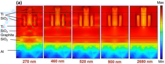
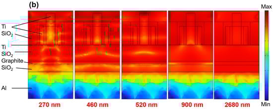
Figure 11.
Intensity distributions of (a) the electric field and (b) the magnetic field, with different normal incident wavelengths.
The evolution of absorption performance of the investigated ultra-wideband optical absorber was evaluated across incident angles ranging from 0° to 90° under TE polarization and TM polarization, as depicted in Figure 12. As Figure 12a shows, TM polarization yielded comparable results and thus is not presented separately. The simulation results depicted in Figure 12 show a curve where absorptivity exceeds 0.900 across a variety of incident wavelengths and angles. Notably, under TE polarization and across the wavelength range from approximately 270 to 4000 nm, absorptivity exhibits significant drops around 420 and 1180 nm when the incident angle exceeds 35° and 38°, respectively. However, for wavelengths between 270 and 4000 nm, absorptivity consistently remains above 0.900 for incident angles ranging from 0° to approximately 45° to 60°. As shown in Figure 12b, under TM polarization, even at an incident ranging from 0° to approximately 40° to 60°, the absorptivity remains above 90% across the 270 to 3600 nm range. This clearly demonstrates that the designed ultra-wideband optical absorber possesses angle-insensitive characteristics, particularly under TM polarization. Its highly symmetrical structure ensures exceptional absorption performance regardless of polarization. This attribute enhances the absorber’s versatility and effectiveness across a wide range of incident angles and polarization states, making it suitable for diverse optical applications.
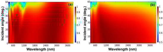
Figure 12.
Absorptivity distribution of (a) TE-polarized light and (b) TM-polarized light with normal direction and various oblique incidence angles.
To evaluate the absorption capacity of the ultra-wideband absorber from UV-B to middle-IR, which utilizes a square hollow embedded in a square cavity in the top layer of multilayer metamaterials for solar energy, Figure 13 presents the computed absorptivity of solar energy across the AM1.5 spectrum, covering a wavelength range of 270 to 4000 nm. Notably, Table 2 compares the average absorptivity within each small wavelength range from 280 to 4000 nm. It clearly shows that the absorptivity of the absorber in each segment is between 90.0% and 98.3%. In the past, many absorbers were unable to extend their absorption bandwidth to include the UV-B or middle-IR ranges. However, the investigated absorber achieves an absorption rate of 95.3% in the wavelength range of 270–400 nm, significantly enhancing overall absorptivity in this specific range. Hence, the investigated absorber demonstrates impressive absorption capabilities under the AM1.5 solar spectrum, achieving an overall absorptivity of 95.7% across the entire wavelength range from 280 to 4000 nm. These findings underscore the absorber’s effectiveness in efficiently capturing solar energy across the UV-B, UV-A, visible, near-infrared (NIR), and middle-IR spectra. This superior absorption performance holds significant promise for applications in solar conversion and energy-harvesting initiatives. The absorber’s nearly ideal wideband absorption across the UV-B to mid-IR range is particularly noteworthy, as it aligns with the high-energy portion of primary solar radiation, making it a highly effective solution for maximizing solar energy utilization. These findings emphasize the potential applications of the designed ultra-wideband optical absorber, establishing it as a valuable component in the pursuit of sustainable energy solutions.
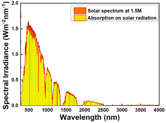
Figure 13.
Absorption spectrum of the investigated absorber with the excavating square matrix cavities in the top SiO2 layer and placing a metal Ti square nanopillar and a metal Ti square hollow inside each cavity.
Table 2.
Absorption characteristics of the designed absorber across various wavelength ranges of the AM1.5 solar spectrum.
To highlight the advantages of this work, Table 3 compares the characteristics of several ultra-wideband absorbers published in the past two years with the results of this study. The techniques used to achieve ultra-wideband absorption and the ranges of these absorbers are also displayed in Table 3. As shown, compared to these broadband solar absorbers, our research shows that the bandwidth of our solar absorber not only achieves an absorptivity exceeding 0.900 over a range up to 270 nm, but also extends to 3600 nm with an absorptivity exceeding 0.900. Moreover, our absorber achieves an average absorptivity of 0.967 in the range of 270–3600 nm. It is evident that the bandwidth of the absorber in this study is slightly wider in the short-wavelength region compared to Ref. [29] (244 nm versus 270 nm). Importantly, for the long-wave infrared range, it surpasses the absorbers designed in Table 3.
Table 3.
A comparison of the characteristics of several ultra-wideband absorbers published in the past two years with our investigated ultra-wideband absorber is provided. Bandwidth refers to the wavelength region where the absorptivity exceeds 0.900.
4. Conclusions
In this study, following the optimization of the structural parameters of our absorber, which featured a metamaterial design incorporating a square nanopillar and a square hollow embedded within the top layer, we consistently achieved absorptivity levels exceeding 0.9 across a wide spectrum ranging from 270 to 3600 nm. Furthermore, the average absorptivity within this wavelength range increased from 0.955 to 0.967 as a result of these optimizations. Within the wavelength range of approximately 400–750 nm, the real part of the impedance for the absorber featuring six continuous planes deviated significantly from unity, while the investigated absorber lacking a square nanopillar and square hollow also showed deviation. Additionally, the imaginary part deviated from zero in both cases. This deviation is primarily responsible for the lower absorptivity observed in absorbers utilizing these structures. The absorption spectrum revealed absorption peaks at 270, 460, 520, 900, and 2680 nm, which were subsequently utilized for analyzing the electric and magnetic fields. The influence of the Fabry–Perot cavity did not appear in the energy distributions of these fields at the five resonance wavelengths. The computed absorptivity of solar energy across the range of 270 nm to 4000 nm clearly indicated that the absorber’s efficiency in each segment ranged between 90.0% and 98.3%, resulting in an overall absorptivity of 95.7% across the entire wavelength range.
Author Contributions
Conceptualization, C.-T.L., P.-X.K., C.-M.H., C.-F.Y. and T.-L.W.; software, C.-T.L., P.-X.K., C.-M.H., C.-F.Y. and T.-L.W.; validation, C.-T.L., P.-X.K., C.-F.Y. and T.-L.W.; formal analysis, C.-T.L., P.-X.K., C.-M.H., C.-F.Y. and T.-L.W.; investigation, C.-T.L., P.-X.K., C.-M.H., C.-F.Y. and T.-L.W.; data curation, C.-T.L., P.-X.K., C.-M.H., C.-F.Y. and T.-L.W.; writing—original draft preparation, C.-T.L., C.-F.Y. and T.-L.W.; writing—review and editing, C.-T.L., C.-F.Y. and T.-L.W.; visualization, C.-T.L., P.-X.K., C.-M.H., C.-F.Y. and T.-L.W. All authors have read and agreed to the published version of the manuscript.
Funding
This research was supported by the Ministry of National Defense of Taiwan for funding support for the “2024 Military Academy Faculty Research Project” and by projects under Nos. NSTC 113-2622-E-390-001 and NSTC 113-2221-E-390-011.
Institutional Review Board Statement
Not applicable.
Informed Consent Statement
Not applicable.
Data Availability Statement
Data are contained within the article.
Acknowledgments
We would be like to thank Pitotech Co., Ltd. for their help in training in the use of COMSOL Multiphysics® software (version 6.0).
Conflicts of Interest
The authors declare no conflicts of interest.
References
- Kocer, H.; Butun, S.; Banar, B.; Wang, K.; Tongay, S.; Wu, J.; Aydin, K. Thermal tuning of infrared resonant absorbers based on hybrid gold-VO2 nanostructures. Appl. Phys. Lett. 2015, 106, 161104. [Google Scholar] [CrossRef]
- Boulvert, J.; Gabard, G.; Romero-García, V.; Groby, J.P. Compact resonant systems for perfect and broadband sound absorption in wide waveguides in transmission problems. Sci. Rep. 2022, 12, 10013. [Google Scholar] [CrossRef] [PubMed]
- Liu, M.; Wang, X.; Xin, F. Sound absorption of acoustic resonant absorbers with rough oblique perforations. Appl. Acoust. 2024, 217, 109828. [Google Scholar] [CrossRef]
- Chaudhuri, K.; Alhabeb, M.; Wang, Z.; Shalaev, V.M.; Gogotsi, Y.; Boltasseva, A. Highly Broadband Absorber Using Plasmonic Titanium Carbide (MXene). ACS Photonics 2018, 5, 1115–1122. [Google Scholar] [CrossRef]
- Yildirim, D.U.; Ghobadi, A.; Soydan, M.C.; Serebryannikov, A.E.; Ozbay, E. One-Way and near-Absolute Polarization Insensitive near-Perfect Absorption by Using an All-Dielectric Metasurface. Opt. Lett. 2020, 45, 2010–2013. [Google Scholar] [CrossRef] [PubMed]
- Tsai, S.T.; Huang, J.L.; Ke, P.X.; Yang, C.F.; Chen, H.C. Analyses of an Ultra-Wideband, Perfectly Absorptive Fractal Absorber with a Central Square Nanopillar in a Cylindrical Structure with a Square Hollow. Materials 2023, 16, 6898. [Google Scholar] [CrossRef]
- Moghaddaszadeh, M.; Ragonese, A.; Hu, Y.; Guo, Z.; Aref, A.; Zhou, C.; Ren, S.; Nouh, M. Local resonance bandgap control in a particle-aligned magnetorheological metamaterial. Commun. Mater. 2023, 4, 94. [Google Scholar] [CrossRef]
- Lobet, M.; Kinsey, N.; Liberal, I.; Caglayan, H.; Huidobro, P.A.; Galiffi, E.; Mejía-Salazar, J.R.; Palermo, G.; Jacob, Z.; Maccaferri, N. New Horizons in Near-Zero Refractive Index Photonics and Hyperbolic Metamaterials. ACS Photonics 2023, 10, 3805–3820. [Google Scholar] [CrossRef] [PubMed]
- Smith, D.R.; Pendry, J.B.; Wiltshire, M.C.K. Metamaterials and Negative Refractive Index. Science 2004, 305, 788–792. [Google Scholar] [CrossRef]
- Cai, Y.; Zhu, J.; Liu, Q.H. Tunable enhanced optical absorption of graphene using plasmonic perfect absorbers. Appl. Phys. Lett. 2015, 106, 043105. [Google Scholar] [CrossRef]
- Patel, S.K.; Surve, J.; Parmar, J.; Nguyen, T.K. Review on Graphene-based Absorbers for Infrared to Ultraviolet Frequencies. J. Adv. Eng. Comput. 2021, 5, 214–238. [Google Scholar] [CrossRef]
- Bidmeshkipour, S.; Akhavan, O. Graphene nanopores in broadband wide-angle optical cavity resonance absorbers. Surf. Interfaces 2022, 30, 101956. [Google Scholar] [CrossRef]
- Liu, J.; Ye, Y.; Deng, L.; Liu, L.; Li, Z.; Liu, F.; Zhou, Y.; Xia, J.; Liu, D. Integrated four-channel directly modulated O-band optical transceiver for radio over fiber application. Opt. Express 2018, 26, 21490–21500. [Google Scholar] [CrossRef] [PubMed]
- Yu, P.; Besteiro, L.V.; Huang, Y.; Wu, J.; Fu, L.; Tan, H.H.; Jagadish, C.; Wiederrecht, G.P.; Govorov, A.O.; Wang, Z. Broadband Metamaterial Absorbers. Adv. Opt. Mater. 2019, 7, 1800995. [Google Scholar] [CrossRef]
- Huang, Y.; Liu, L.; Pu, M.; Li, X.; Ma, X.; Luo, X. A refractory metamaterial absorber for ultra-broadband, omnidirectional and polarization-independent absorption in the UV-NIR spectrum. Nanoscale 2018, 10, 8298–8303. [Google Scholar] [CrossRef]
- Tharwat, M.M.; Alsulami, A.R.; Mahros, A.M. Exploring the Absorption Spectra of an Ultra-Wideband Metamaterial Absorber in the Visible and Near-Infrared Regions. Materials 2022, 15, 7160. [Google Scholar] [CrossRef]
- Hakim, M.L.; Hanif, A.; Alam, T.; Islam, M.T.; Arshad, H.; Soliman, M.S.; Saleh Albadran, M.; Islam, M.S. Ultrawideband Polarization-Independent Nanoarchitectonics: A Perfect Metamaterial Absorber for Visible and Infrared OpticalWindow Applications. Nanomaterials 2022, 12, 2849. [Google Scholar] [CrossRef] [PubMed]
- Sun, C.; Liu, H.; Yang, B.; Zhang, K.; Zhang, B.; Wu, X. An ultra-broadband and wide-angle absorber based on a TiN metamaterial for solar harvesting. Phys. Chem. Chem. Phys. 2023, 25, 806–812. [Google Scholar] [CrossRef]
- Peng, G.; Ke, P.X.; Tseng, L.C.; Yang, C.F.; Chen, H.C. The Design of a Multilayer and Planar Metamaterial with the Multi-Functions of a High-Absorptivity and Ultra-Broadband Absorber and a Narrowband Sensor. Photonics 2023, 10, 804. [Google Scholar] [CrossRef]
- Sreekanth, K.V.; Han, S.; Singh, R. Ge2Sb2Te5—Based tunable perfect absorber cavity with phase singularity at visible frequencies. Adv. Mater. 2018, 30, 1706696. [Google Scholar] [CrossRef]
- Ullah, H.; Khan, A.D.; Noman, M.; Rehman, A.U. Novel Multi-Broadband Plasmonic Absorber Based on a Metal-Dielectric-Metal Square Ring Array. Plasmonics 2018, 13, 591–597. [Google Scholar] [CrossRef]
- Guo, T.L.; Li, F.; Roussey, M. Dielectric Cavity-Insulator-Metal (DCIM) Metamaterial Absorber in Visible Range. Nanomaterials 2023, 13, 1401. [Google Scholar] [CrossRef] [PubMed]
- Zhang, S.; Wang, Y.; Wang, S.; Zheng, W. Wavelength-tunable perfect absorber based on guided-mode resonances. Appl. Opt. 2016, 55, 3176–3181. [Google Scholar] [CrossRef] [PubMed]
- Cao, S.; Zhang, D.; Wang, Q. Graphene-based dynamically tunable absorbers through guided mode resonance. Superlattices Microstruct. 2020, 144, 106550. [Google Scholar] [CrossRef]
- Qing, Y.M.; Ma, H.F.; Yu, S.; Cui, T.J. Ultra-narrowband absorption enhancement in monolayer transition-metal dichalcogenides with simple guided-mode resonance filters. J. Appl. Phys. 2019, 125, 213108. [Google Scholar] [CrossRef]
- Park, C.Y.; Lee, K.Y.; Choi, Y.S.; Yoon, J.W. Compact coherent perfect absorbers using topological guided-mode resonances. Sci. Rep. 2024, 14, 14144. [Google Scholar] [CrossRef]
- Szabo, Z.; Park, G.; Hedge, R.; Li, E. A Unique Extraction of Metamaterial Parameters Based on Kramers–Kronig Relationship. IEEE Trans. Microwave Theory Tech. 2010, 5, 2646–2653. [Google Scholar] [CrossRef]
- Liao, S.H.; Wang, C.H.; Ke, P.X.; Yang, C.F. Using Planar Metamaterials to Design a Bidirectional Switching Functionality Absorber—Ultra-Wideband Optical Absorber and Multi-Wavelength Resonant Absorber. Photonics 2024, 11, 199. [Google Scholar] [CrossRef]
- Wu, F.; Shi, P.; Yi, Z.; Li, H.; Yi, Y. Ultra-Broadband Solar Absorber and High-Efficiency Thermal Emitter from UV to Mid-Infrared Spectrum. Micromachines 2023, 14, 985. [Google Scholar] [CrossRef]
- Peng, G.; Li, W.Z.; Tseng, L.C.; Yang, C.F. Investigation of a Multi-Layer Absorber Exhibiting the Broadband and High Absorptivity in Red Light and Near-Infrared Region. Nanomaterials 2023, 13, 766. [Google Scholar] [CrossRef]
- Ehsanikachosang, M.; Karimi, K.; Rezaei, M.H.; Pourmajd, H. Metamaterial solar absorber based on titanium resonators for operation in the ultraviolet to near-infrared region. J. Opt. Soc. Am. B 2022, 39, 3178–3186. [Google Scholar] [CrossRef]
- Wang, Y.; Liu, F.; Ni, B.; Chen, L.; Ji, K. Design of an ultra-wideband solar absorber based on tungsten. AIP Adv. 2023, 13, 095024. [Google Scholar] [CrossRef]
Disclaimer/Publisher’s Note: The statements, opinions and data contained in all publications are solely those of the individual author(s) and contributor(s) and not of MDPI and/or the editor(s). MDPI and/or the editor(s) disclaim responsibility for any injury to people or property resulting from any ideas, methods, instructions or products referred to in the content. |
© 2024 by the authors. Licensee MDPI, Basel, Switzerland. This article is an open access article distributed under the terms and conditions of the Creative Commons Attribution (CC BY) license (https://creativecommons.org/licenses/by/4.0/).