Abstract
With the rapid development of optical communication and quantum information, the demand for efficient and broadband nonlinear frequency conversion has increased. At present, most single-frequency conversion processes in lithium niobate on insulator (LNOI) waveguides suffer from lateral leakage without proper design, leading to an additional increase in propagation loss. Achieving broadband frequency conversion also encounters this problem in that there are no relevant works that have solved this yet. In this paper, we theoretically propose an efficient and flat broadband second harmonic generation (SHG) in silicon nitride loaded apodized chirped periodically poled LNOI waveguides. By using a bound states in the continuum (BICs) mechanism to reduce the propagation loss and utilizing the characteristic that the BICs are insensitive to wavelength, an ultra-low-loss wave band of 80 nm is realized. Then, by employing an apodized chirped design, a flat broadband SHG is achieved. The normalized conversion efficiency (NCE) is approximately 222%W−1cm−2, and the bandwidth is about 100 nm. Moreover, the presented waveguides are simple and can be fabricated without direct etching of lithium niobate, exhibiting excellent fabrication tolerance. Our work may open a new avenue for exploring low-loss and flat broadband nonlinear frequency conversion on various on-chip integrated photonic platforms.
1. Introduction
As the “silicon” in nonlinear optics, lithium niobate is widely recognized as one of the most popular optical materials because of its large second-order nonlinear coefficients (d33 = 27.4 pm/V) and wide transparency window (350 nm–4.5 μm) [1]. In recent years, except for some other nonlinear materials, LNOI has emerged as an exceptional platform for research and applications of nonlinear optics [2,3,4,5,6]. Thus, it finds extensive applications in second-order nonlinear optics, including second harmonic generation, sum frequency generation (SFG), and difference frequency generation (DFG) [7,8,9,10,11]. Due to nanophotonic waveguides based on LNOI exhibiting tight confinement of the modal field, it can significantly enhance the interaction between light and matter, thus the NCE is increased by more than an order of magnitude, in comparison to bulk lithium niobate waveguides based on proton exchange or titanium diffusion [12,13]. Recently, various efficient nonlinear frequency conversion processes have been realized in compact nanophotonic devices, such as loaded waveguides [14,15], etched waveguides [16,17,18], microring and microdisk resonators [19,20,21,22].
At present, waveguide structures based on LNOI, whether etched waveguides or loaded waveguides, may exhibit lateral leakage of waveguide mode when the effective refractive index of the bound mode is lower than that of the orthogonally polarized continuous mode in the slab [23]. Particularly, for a given rib height, lateral leakage is more likely to occur when the thickness of the slab layer is larger or at a shorter wavelength. For instance, in order to apply the maximum nonlinear coefficient of lithium niobate, d33, TE polarization is usually chosen for X-cut LNOI waveguides. Since the effective refractive index of the TE bound mode for the second harmonic (SH) wave may be lower than that of the TM continuous mode, these two modes will couple, causing the energy of the bound mode to dissipate towards the continuous mode and resulting in lateral leakage. Similarly, TM polarization is employed in Z-cut LNOI waveguides, where the TM bound mode for both fundamental frequency (FF) and SH waves may exhibit lateral leakage. Hence, it is imperative to consider the lateral leakage in LNOI waveguides owing to its impact on introducing non-negligible propagation loss, affecting overall conversion efficiency of devices [23,24,25].
In general, by changing the structural parameters of etched waveguides such as lithium niobate thickness, etching depth, and waveguide top width, the effective refractive index of the bound mode can surpass that of the orthogonally polarized continuous mode, resulting in no lateral leakage. Therefore, when designing etched waveguides based on LNOI, lateral leakage can be suppressed through choosing LNOI with a thinner lithium niobate layer. If designing specific structures requires a fixed thickness of the lithium niobate layer, lateral leakage can also be suppressed by increasing the etched depth. For example, Andreas Boes et al. discovered lateral leakage of the SH wave in the X-cut LNOI waveguides investigated by Chang Lin and solved this problem by selecting an appropriate waveguide structure, thereby reducing the propagation loss and achieving higher NCE of SHG [25]. Similarly, Xina Wang et al. considered the impact of lateral leakage when designing the waveguide structures for their study on quantum frequency conversion based on Z-cut LNOI [26].
For loaded waveguides, the design of low-refractive-index waveguide structures on high-refractive-index substrates enables the realization of BICs, which has been demonstrated as an effective way to suppress lateral leakage [27,28]. By carefully designing the waveguide width, destructive interference occurs between the loss channel of the bound mode and its orthogonally polarized continuous mode. Thus, the bound mode and continuous mode decouple, making the bound mode become lossless and then improving overall conversion efficiency. For instance, the BICs mechanism is employed to reduce the propagation loss of FF and SH waves, resulting in efficient SHG in etchless LNOI waveguides [29,30].
In recent years, the study of broadband frequency conversion is ongoing, because it can achieve all-optical wavelength conversion and construct multi-channel wavelength division multiplexing systems that satisfy the demand for high-capacity optical communication. For example, broadband SHG converters are widely applied in optical networks and ultra-fast optical signal processing [31,32,33]. As we know, there are mainly two ways to realize broadband SHG: the first is dispersion engineering (DE), by carefully designing the waveguide structures to achieve group velocity matching and even zero group velocity dispersion between FF and SH waves. The second is chirped periodic poling (CPP), by setting multiple regions with varying poling periods that correspond to different phase-matched wavelengths, accumulating a broadband SHG along the waveguide [34,35,36].
Broadband SHG based on LNOI waveguides also exhibits lateral leakage. By employing DE on LNOI etched waveguides, a broadband spectrum was generated, but suffered from lateral leakage at short wavelengths [37,38]. Although DE offers advantages in simultaneously ensuring efficiency and bandwidth, it remains challenging to find a proper design that satisfies zero group velocity dispersion and no lateral leakage at the same time because both requirements need to optimize the structures [39]. For broadband SHG based on CPP, the issue of lateral leakage, or the propagation loss, is more important. Since only a small periodically poled region converts the matched wavelength along the entire waveguide, almost no frequency conversion occurs in other positions but only propagation. Consequently, the propagation loss of SH wave significantly impacts the NCE of broadband SHG. By employing CPP on LNOI etched waveguides, broadband SHG is achieved with undesirable fluctuations, and the waveguide loss is over 9 dB/cm mainly arising from the rough sidewall [39]. Additionally, obtaining etched waveguide with low loss in LNOI is not trivial, which requires expensive equipment and substantial effort in process development.
Therefore, it is important to reduce the propagation loss when utilizing CPP to realize broadband SHG. To the best of our knowledge, there are no relevant works solving the propagation loss of broadband SHG. In this work, based on the BICs mechanism effectively suppressing the lateral leakage of the SH wave and utilizing apodized chirp to remove the fluctuations of broadband spectrum, we propose a silicon nitride loaded apodized chirped periodically poled LNOI waveguide, achieving an efficient and flat broadband SHG. The NCE is approximately 222%W−1cm−2t and the bandwidth is about 100 nm, which is comparable to the performance of LNOI etched waveguides. In addition, our proposed waveguide is simple and achieved without directly etching lithium niobate, making it relatively easy to fabricate with high fabrication tolerance, providing a novel way to produce low-loss and flat broadband SHG.
2. Theory and Design
2.1. Design of Waveguide Structure
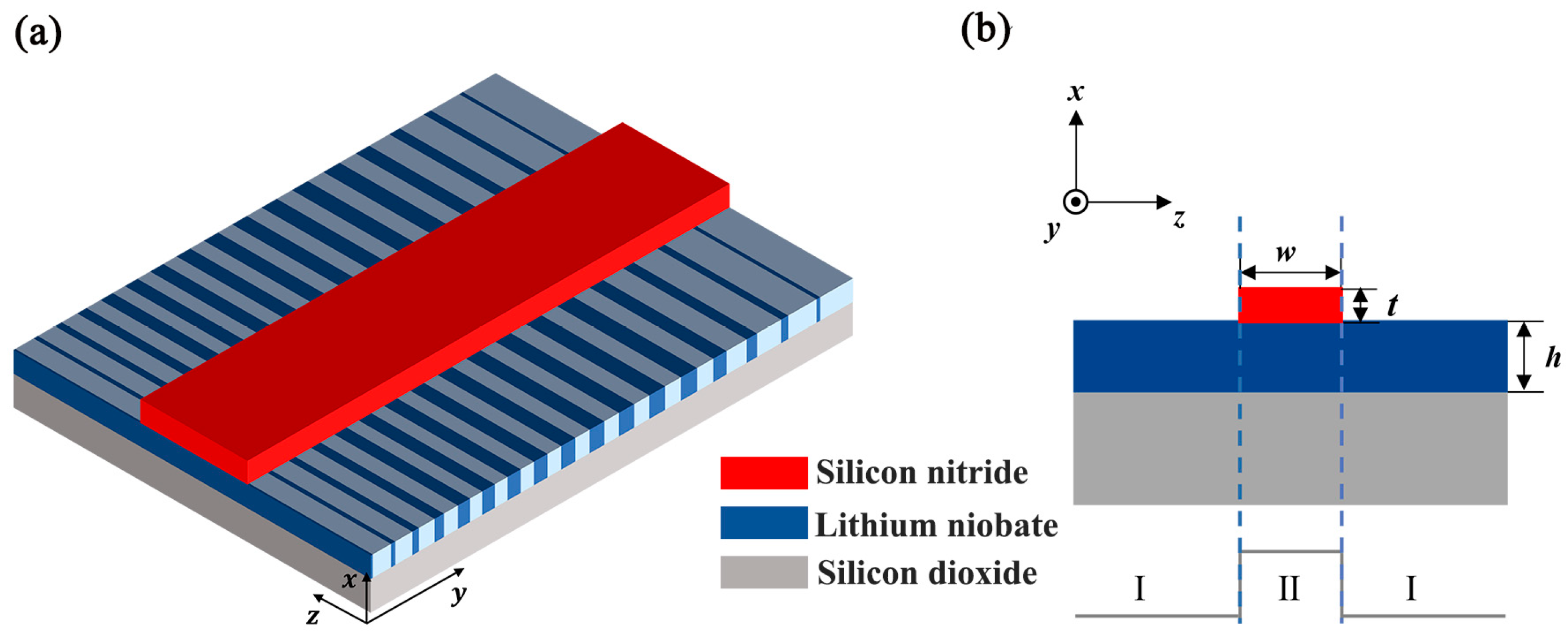
Figure 1a,b are the three-dimensional schematic and cross-sectional illustration of the proposed waveguide, respectively. The silicon nitride layer with a thickness of t = 200 nm is deposited on LNOI by using inductively coupled plasma chemical vapor deposition (ICPCVD) and then etched to form a waveguide with a width of w = 1.62 μm through reactive ion etching (RIE). The LNOI consists of a X-cut lithium niobate thin film with a thickness of h = 600 nm and a 2 μm-thick silicon dioxide layer (NANOLN). By adding silicon nitride to LNOI, it can form region II, in which the effective refractive index is higher than that in the two sides region I, thereby forming an optical waveguide.

Figure 1.
(a) Three-dimensional structure diagram of silicon nitride loaded apodized chirped periodically poled LNOI waveguide, consisting of a silicon nitride waveguide, X-cut lithium niobate thin film and silicon dioxide substrate. (b) Schematic diagram depicting the z-x cross section of waveguide structure, where w and t denote the width and thickness of the silicon nitride waveguide respectively, and h represents the thickness of the lithium niobate thin film.
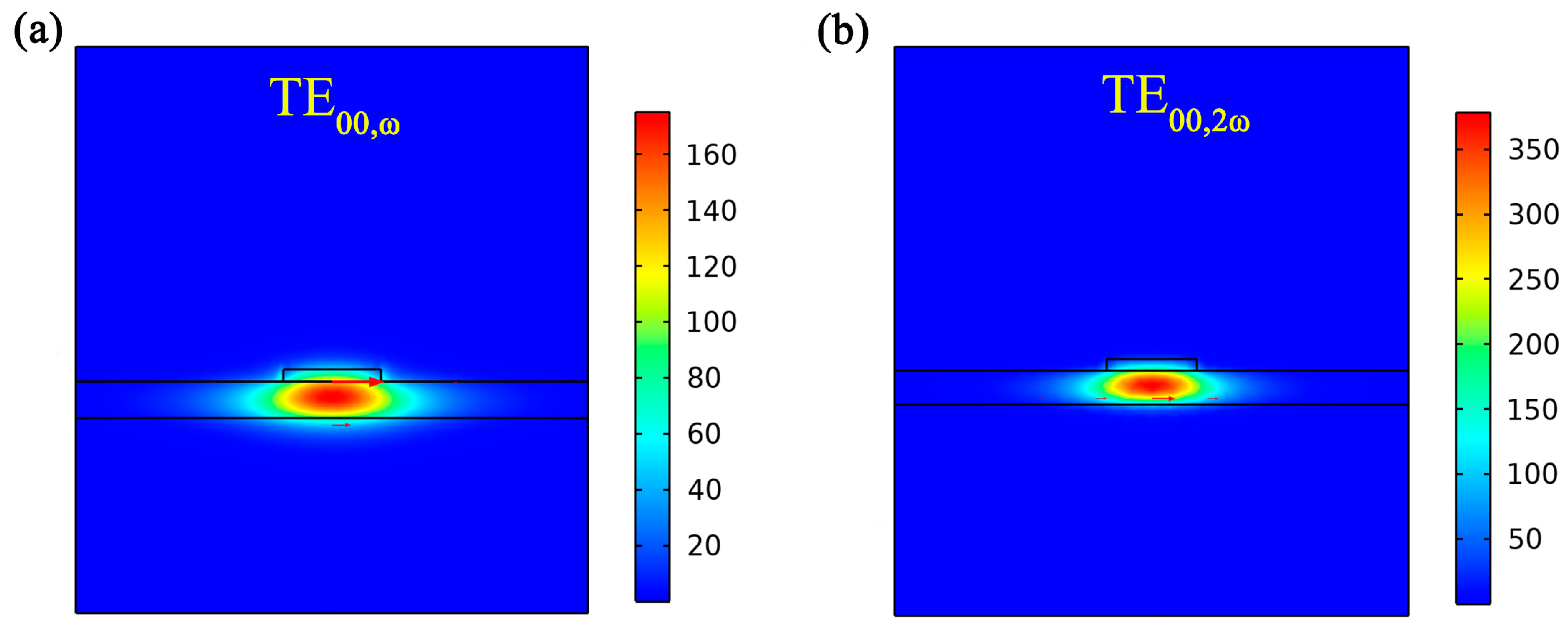
In X-cut LNOI, TE modes are often chosen to utilize the maximum nonlinear coefficient d33 and thus enhance the SHG efficiency. The modal field distribution of TE fundamental modes for the FF wave at 1600 nm and the SH wave at 800 nm are shown in Figure 2. Due to the high-refractive-index region II, both FF and SH waves are well confined in lithium niobate thin film so that the large nonlinear modal overlap can be obtained.
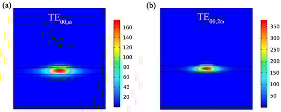
Figure 2.
The modal field distribution of TE bound mode for (a) FF wave at 1600 nm and (b) SH wave at 800 nm.
2.2. Broadband Waveguide BICs
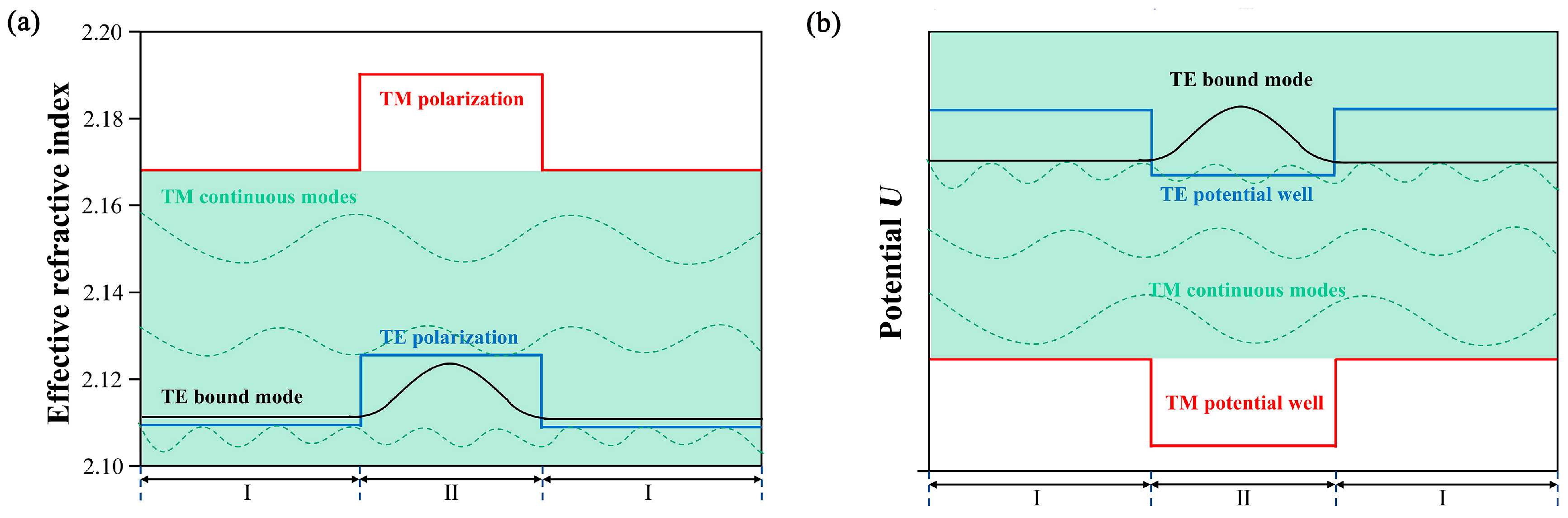
By comparing the Schrödinger equation and wave equation, the potential of photons can be defined as −n2k2, where n represents the refractive index and k denotes the wave vector. Figure 3a,b depict the effective refractive index distribution and photonic potential distribution of SH wave, respectively. Since the effective refractive index of the TE bound mode is lower than that of the TM continuous mode, it leads to a higher potential for the TE bound mode. As a result, the TE bound mode will easily couple with the TM continuous mode and cause lateral leakage, causing an increased propagation loss of the SH wave. It should be noted that the TE bound mode of the FF wave will not evolve to the TM continuous mode since the effective refractive index of the TE bound mode for the FF wave is larger than that of the TM bound mode. Therefore, only the lateral leakage of the SH wave needs to be considered.
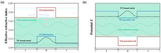
Figure 3.
(a) Effective refractive index distribution of SH wave at 800 nm in region I and II. The red line represents the refractive index distribution of TM mode, the blue line represents the refractive index distribution of TE mode, the green part represents the TM continuous modes, and the black line represents the TE bound mode in the TM continuous modes. (b) The photonic potential distribution of SH wave at 800 nm. The potential well of TE mode is higher than that of TM mode.
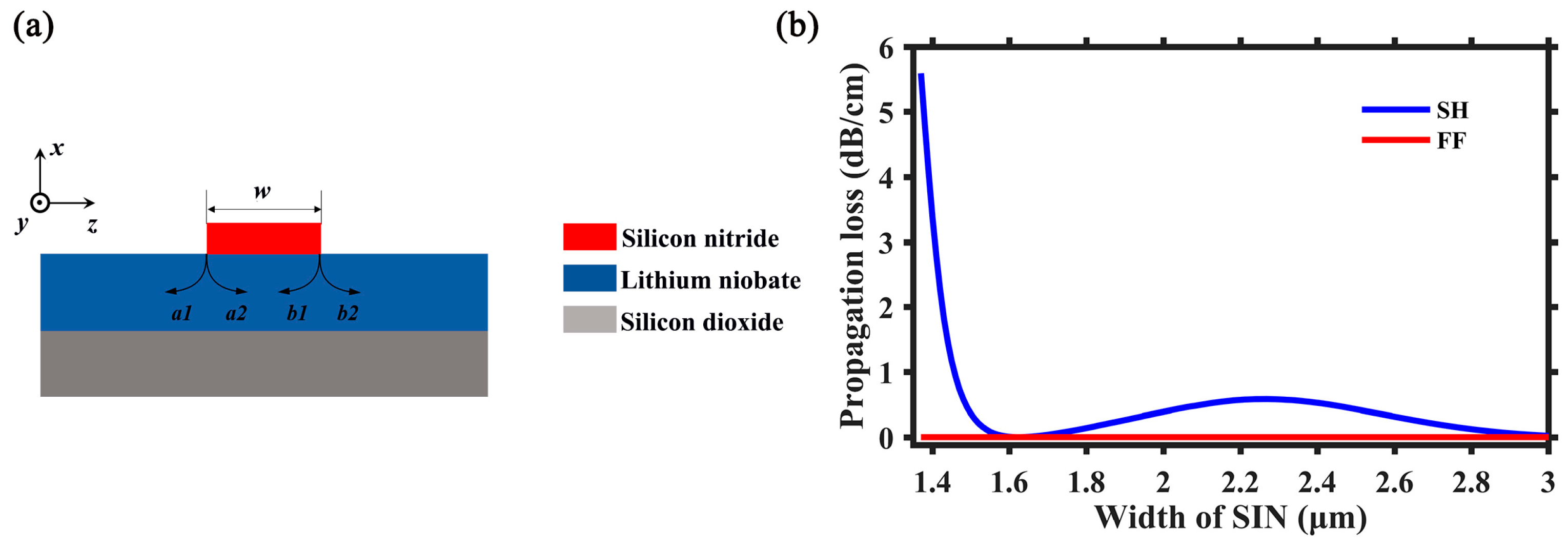
Figure 4a shows the interaction between the TE bound mode and the TM continuous mode of the SH wave. When the TE bound mode couples with the TM continuous mode, it dissipates energy to the continuous mode through the left channels (a1 and b1) and right channels (a2 and b2) at the edge of the waveguide, resulting in energy loss of the bound mode. While by carefully designing the waveguide width w, it can achieve destructive interference between the coupled channels a1 (a2) and b1 (b2), leading to decoupling of the bound mode and continuous mode. According to the analysis [27,28], the attenuation length L of the SH wave in the TE bound mode can be expressed as:
where kz is the z component of the TM continuous mode wave vector of the SH wave and w is the waveguide width. By appropriately designing the waveguide width w so that kzw equals an odd multiple of π, the attenuation length L of the SH wave tends to infinity, so the TE bound mode of the SH wave becomes lossless BICs. Figure 4b shows the propagation loss of the FF and SH waves of the TE bound mode as a function of the width w of the silicon nitride waveguide. Obviously, the propagation loss of the FF wave in the TE bound mode is zero, while it varies with the waveguide width w for the SH wave, consistent with the analysis in the previous paragraph. When the waveguide width is w = 1.62 μm, the TE bound mode achieves a minimum propagation loss, indicating it is a BICs mechanism. Therefore, the silicon nitride waveguide is designed with a width of w = 1.62 μm.
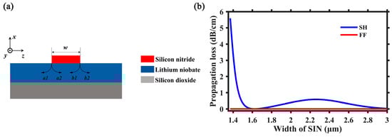
Figure 4.
(a) Dissipated channels of bound mode to continuous mode. (b) The propagation loss of FF and SH waves in TE bound mode varies with silicon nitride waveguide width w. At width w = 1.62 μm, the propagation loss reaches minimum, indicating the BICs.
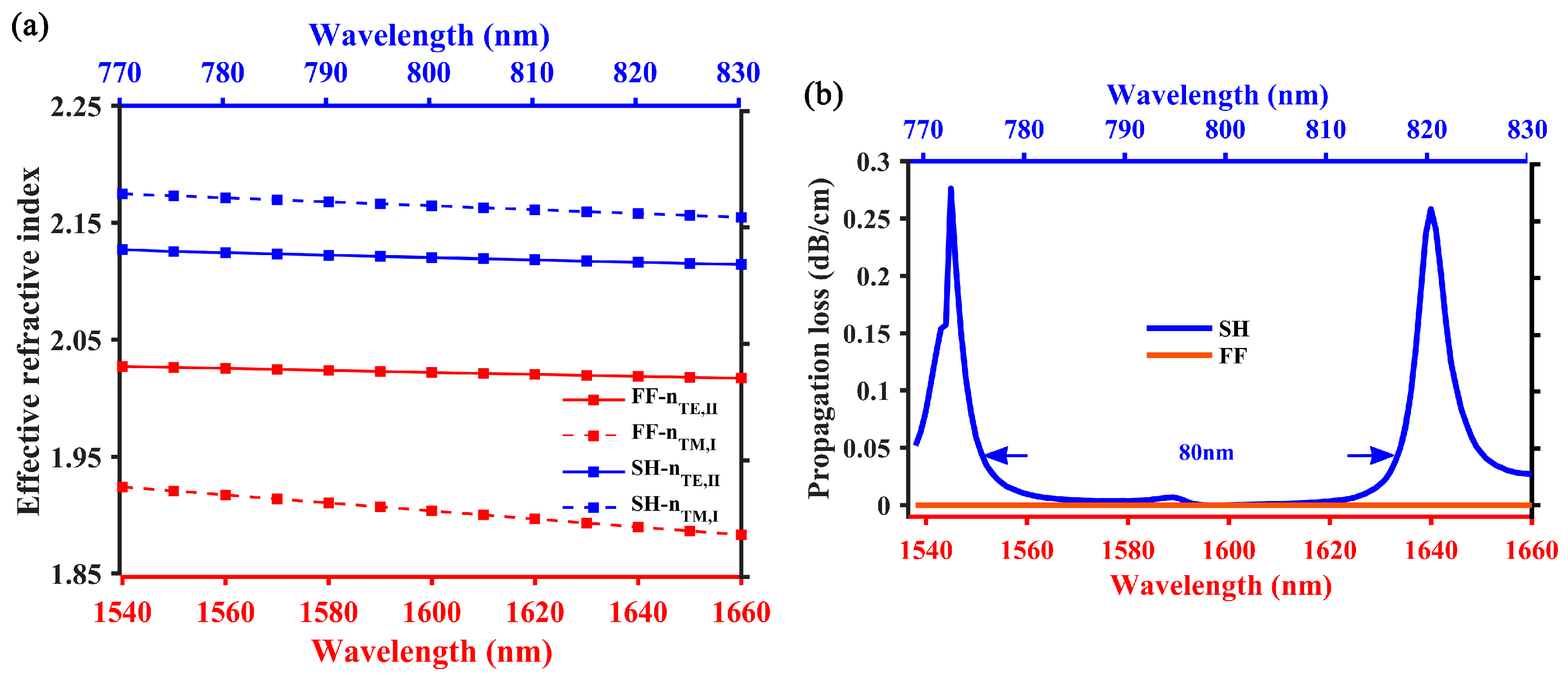
Recently, relevant research has pointed out that waveguide BICs have the characteristic of being insensitive to wavelength [28,29,30]. According to Equation (1), because of the kzw, waveguide BICs depend on wavelength and waveguide width w. Actually, the waveguide BICs are mainly affected by the variation of waveguide width w. When the waveguide width w is constant, the waveguide BICs are indeed affected by the variation of wavelength, however, just resulting in very small increase of propagation loss across the entire band. Therefore, it indicates that waveguide BICs have the characteristic of being insensitive to wavelength. In this paper, the designed waveguide structure also exhibits ultra-low propagation loss within a specific band. Figure 5a,b are the effective refractive index and the propagation loss as a function of wavelength, respectively, the corresponding FF wave band is 1540–1660 nm and the SH wave band is 770–830 nm. Since the effective refractive index of the TE bound mode in the FF wave band is higher than that of the TM continuous mode, so the propagation loss caused by the lateral leakage is zero. Although the effective refractive index of the TE bound mode in the SH wave band is lower than that of the TM continuous mode, it maintains a low propagation loss across the entire band. Even at the peak, the propagation loss is less than 0.3 dB/cm, which confirms the insensitivity of waveguide BICs to wavelength. In fact, the peak of propagation loss can be considered as quasi-BICs, which formed due to the wavelength deviating from 800 nm. When compared with non-BICs, quasi-BICs still exhibit small propagation loss.
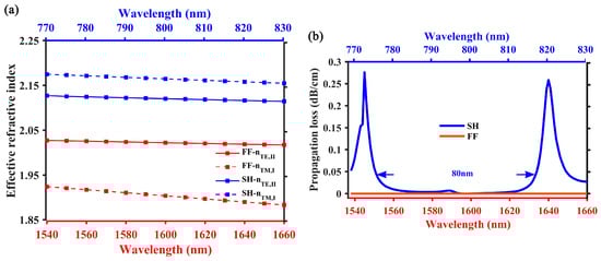
Figure 5.
(a) The effective refractive index of FF and SH waves varies with wavelength. (b) The TE bound mode propagation loss of FF and SH waves varies with wavelength; the red line and blue line represent the propagation loss of FF and SH waves, respectively. The propagation loss of SH wave is less than 0.05 dB/cm within a bandwidth of 80 nm from 1554 nm to 1634 nm.
2.3. Apodized Chirped Periodically Poled Design
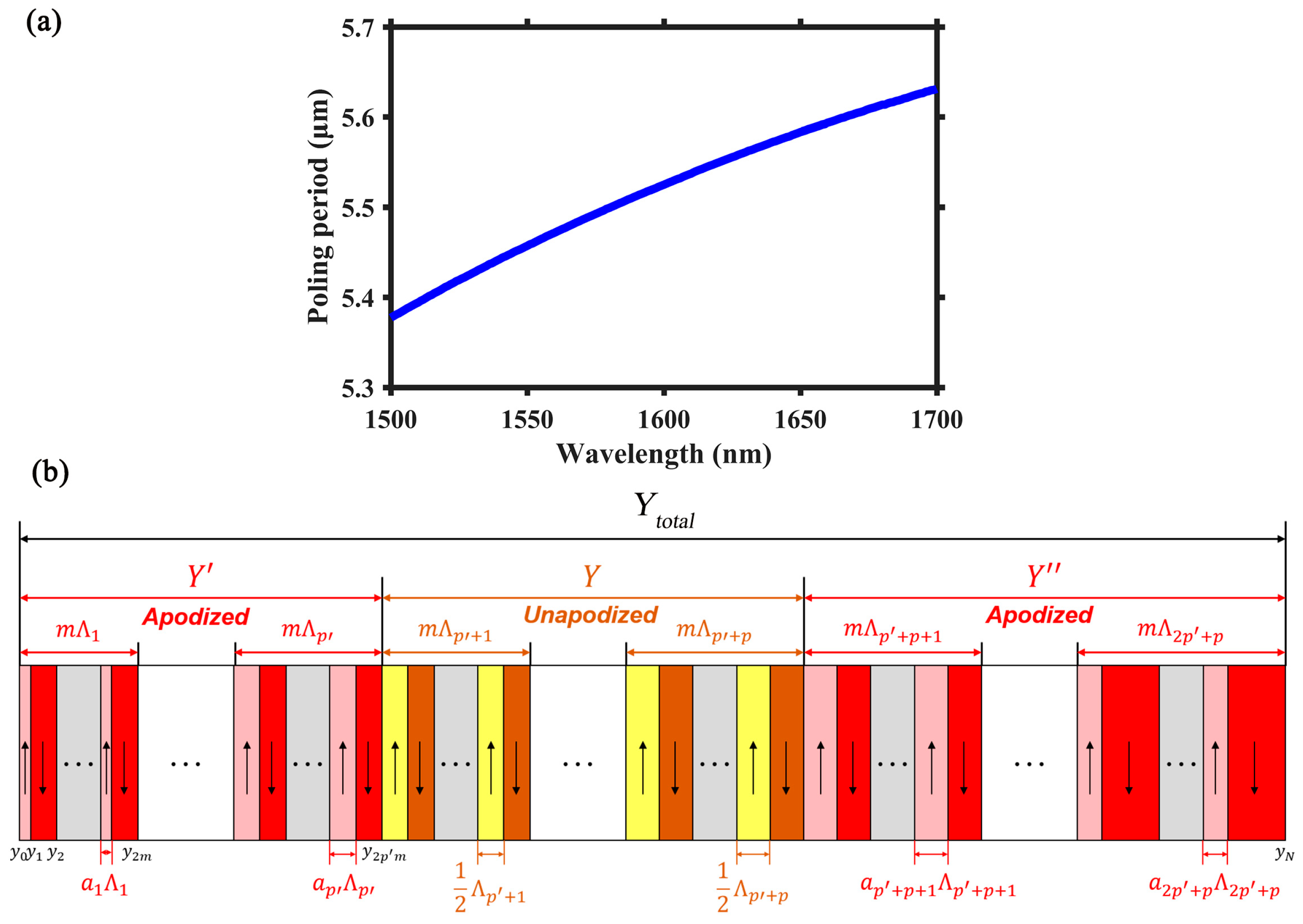
In this paper, the band of 1554–1634 nm with propagation loss less than 0.05 dB/cm is chosen as an example for efficient broadband SHG with apodized chirped periodically poled design. It should be noted that the working band can be freely selected based on different requirements and is not limited to the one selected here. In order to make the working wavelength of broadband SHG cover the ultralow-loss band, we design a step-chirped periodically poled structure in the band of 1510–1690 nm. The total length of the poling region is Ytotal = 0.2 cm, divided into several sections, each containing m fixed poling periods Λ. The poling period difference between adjacent sections is 6 nm, i.e., Λi+1 − Λi = 6 nm. Figure 6a is the poling period Λ required for quasi phase matching as a function of FF wave, Λ = λ/2∆n, where λ represents the FF wavelength, and ∆n denotes the difference of the effective refractive index between the FF and SH waves in the TE bound modes. When the FF wavelength increases from 1510 nm to 1690 nm, the poling period increment is approximately 240 nm, showing a basically linear growth process. Consequently, the poling region is divided into 41 sections.

Figure 6.
(a) The poling period required for quasi phase matching when the FF wavelength changes. (b) Schematic diagram of apodized step-chirped periodically poled structure. Arrows represent the poling direction of lithium niobate thin film.
Although the step-chirped design enables us to broaden the phase matching bandwidth, it leads to ripples in the broadband SHG spectrum. Here, we introduce apodization in the step-chirped design to remove the ripples, achieving a nearly flattop broadband SHG response [40,41,42]. The total length Ytotal has been divided into three regions. The central region with the length of Y is unapodized and composed of p sections with an equal duty-cycle of 1/2. Each of the two adjacent regions are apodized and consist of p′ sections. At the input apodized region with the length of Y′, the duty-cycle for each section is ai = i/2p′, (i = 1, 2, …, p′), i.e., the duty-cycle changes from 1/2p′ to 1/2. Symmetrically, at the output apodized region with the length of Y″, the duty-cycle for each section changes from 1/2 to 1/2p′. The apodization ratio is defined as R = (Y′ + Y″)/Ytotal. Figure 6b illustrates the schematic diagram of an apodized step-chirped periodically poled structure with Ytotal = 0.2 cm, p = 11, p′ = 15, m = 9 and R = 0.73. All simulation results are carried out via the mode analysis in the COMSOL Multiphysics 5.6 software.
3. Results and Discussion
3.1. Conversion Efficiency
In the case of quasi phase matching and without considering propagation loss, the NCE of SHG can be expressed as [29]:
where and c are respectively permittivity and light speed in a vacuum, d33 is the nonlinear coefficient of lithium niobate, nω and n2ω are the effective refractive index of FF and SH waves, respectively, and is FF wavelength. is the spatial modal field overlap between FF and SH waves, defined as:
where denotes two-dimensional integration over the lithium niobate thin film. and are, respectively, the electric fields of the TE bound mode of FF and SH waves. In Equation (2), is the effective modal area with
where denotes two-dimensional integration over all space. For the proposed waveguide, when the FF wavelength is 1600 nm, the simulation results show , , exhibiting high spatial modal overlap and tight confinement of the modal field. In Equation (2), G(λ) is the Fourier transform of function of d(y), d(y) = ±1 denoting the symbol for nonlinear coefficient of lithium niobate after periodic poling. G2(λ) is expressed as:
where is the wave vector mismatch, and and are wave vectors for the FF and SH waves, respectively. As shown in Figure 6b, the apodized chirped periodically poled structure has N = 2(2p′ + p)m domains, and each domain is between yq−1 and yq (q = 1, 2, …, N), which can arrive at [39]:
Equation (5) determines the bandwidth of broadband SHG.
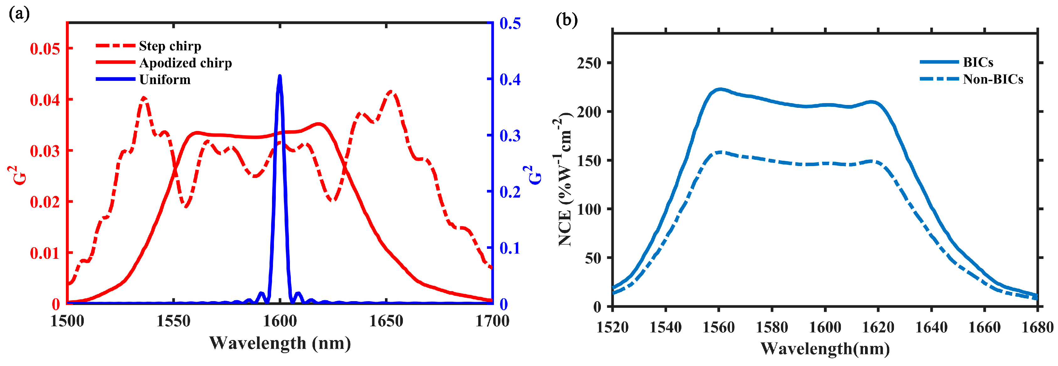
Figure 7a shows the G2(λ) curves of silicon nitride loaded LNOI waveguides with step-chirped period poling, apodized chirped periodic poling and uniform periodic poling. Under the same waveguide parameters, the SHG bandwidth corresponding to step and apodized chirp is significantly larger than that corresponding to uniformly single-period poling. Although the bandwidth of the step-chirped design is larger than the apodized chirp design, it suffers from significant ripples in the broadband SHG spectrum. These ripples cause the output of SH power to vary with wavelength, leading to difficulty in stabilizing the output power.
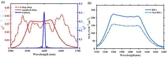
Figure 7.
(a) The red line and the blue line represent respectively the G2 curves corresponding to chirped periodic poling and uniformly single-period poling with the same waveguide parameters, where the dotted and solid red line represent respectively the step chirp and apodized chirp. (b) The NCE of broadband SHG considering the propagation loss. The blue line represents BICs with waveguide width of w = 1.62 μm, and the red line represents non-BICs with waveguide width of w = 1.30 μm.
As depicted in Figure 5b, the propagation loss of the FF band is almost zero, and the SH band is BICs. When calculating the NCE of broadband SHG, it is essential to consider the propagation loss of the SH wave. Based on Equation (1), after considering propagation loss, the NCE of broadband SHG is shown in Figure 7b, which can be expressed as η = ηSHG g(Ytotal). g(Ytotal) is the loss factor and given by [43]:
where αω and α2ω are propagation loss in units of cm−1 of the FF and SH waves, respectively, and ∆α = α2ω/2−αω. As shown in Figure 7b, for the designed silicon nitride loaded LNOI waveguide width of w = 1.62 μm, the ultralow-loss band 1554–1634 nm in BICs almost concentrates on the flattop region with the NCE over 200%W−1cm−2. The maximum NCE reaches 222%W−1cm−2, and the bandwidth approaches 100 nm, which are equivalent to or better than the performance of the etched LNOI waveguides. Moreover, without the use of the BICs mechanism to reduce the propagation loss, such as the waveguide width is w = 1.30 μm, the NCE is about 65% lower than that of BICs. Table 1 is the comparison of the previously reported works of broadband SHG based on LNOI. In terms of bandwidth and NCE, this work is superior to various types of lithium niobate waveguides applying DE to realize broadband SHG, and it is comparable to the performance of LNOI etched waveguides utilizing CPP.

Table 1.
Comparison of the previously reported broadband SHG based on LNOI.
3.2. Fabrication Tolerance
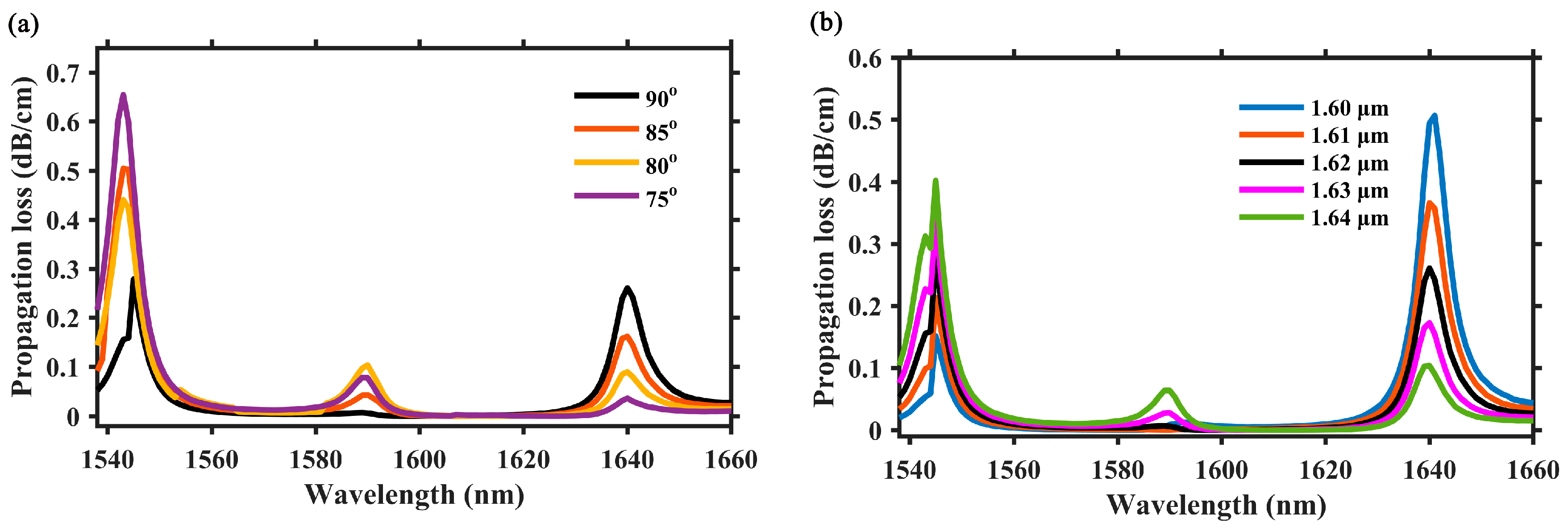
The design of broadband SHG relies on accurate etching of the silicon nitride layer, so the fabrication tolerance is a key issue. When forming a silicon nitride loaded waveguide, the main tolerances to be considered are etched sidewall angle and width. Figure 8a shows the simulated result of propagation loss at different wavelengths when altering an etched sidewall angle. As the etched sidewall angle decreases, the propagation loss gradually increases, while this increase is not significant. Even at the minimum etched sidewall angle of 75°, the propagation loss remains below 0.1 dB/cm within the band of 1554–1634 nm. Figure 8b illustrates the variation in propagation loss at different wavelengths as the silicon nitride loaded waveguide width w is altered. When deviating from the designed width w = 1.62 μm, the propagation loss will increase with the increase of width deviation. Similarly, this increase is slow. When waveguide width w deviates from designed width by ±20 nm, the propagation loss is less than 0.1 dB/cm in the band of 1554–1634 nm. The width tolerance of ±20 nm in experimentation is completely within the currently etching accuracy range of silicon nitride loaded waveguide, indicating sufficient width tolerance for the designed waveguide in this paper. When the etched sidewall angle and width of silicon nitride waveguide change, due to the deviation from waveguide BICs, three peaks occur in Figure 8. Although the propagation loss increases, it maintains a low level across the entire band. In fact, the peak of propagation loss can be considered as quasi-BICs, which are formed due to the waveguide deviating from the designed structure. Compared with non-BICs, quasi-BICs still exhibit small propagation loss. In summary, the silicon nitride loaded waveguide presented in this work exhibits exceptional robustness and can be easily implemented in experiments.
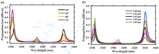
Figure 8.
Fabrication tolerance of (a) etched sidewall angle and (b) width of silicon nitride loaded waveguides.
4. Conclusions
In summary, by using the BICs mechanism to solve the lateral leakage problem and thus reduce the propagation loss of the SH wave and employing an apodized chirp to flatten the broadband spectrum, an efficient and flat broadband SHG is demonstrated in our theoretically proposed silicon nitride loaded apodized chirped periodically poled LNOI waveguides. The maximum NCE is 222%W−1cm−2 and the bandwidth is ~100 nm, which are comparable to or better than the performance of the directly etched LNOI waveguides. The presented waveguides also exhibit excellent fabrication tolerance, meeting current fabrication technology for the etched sidewall angle and width of the silicon nitride waveguides.
It is worthwhile to note that loaded waveguides are more susceptible to femtosecond pulse damage compared to etched waveguides. Our work could still find applications such as SHG of multi-wavelength continuous wave for high-capacity optical communication and signal processing. In addition, the NCE of our broadband SHG would be further improved by reducing the effective modal area of the FF and SH waves, for example, through reducing the thickness of lithium niobate thin film or increasing the thickness of the silicon nitride waveguide layer. Furthermore, the polymer could be selected as the material of the waveguide layer to avoid etching silicon nitride, achieving a completely etchless fabrication process. With high NCE, broad bandwidth and simple design, our work paves a new way to realize low-loss and flat broadband frequency conversion on chips.
Author Contributions
Conceptualization, F.M. and J.H.; methodology, F.M. and J.H.; investigation, software, J.H. and M.L.; writing—original draft preparation, J.H.; writing—review and editing, F.M.; supervision, F.M.; project administration, F.M.; funding acquisition, F.M. All authors have read and agreed to the published version of the manuscript.
Funding
National Natural Science Foundation of China (62105374); Basic and Applied Basic Research Foundation of Guangdong Province (2023A1515012723, 2023B1515040023); Guangzhou Municipal Science and Technology Bureau (2024A04J2004, 202102021157); Fundamental Research Funds for the Central Universities, Sun Yat-sen University (23qnpy59).
Institutional Review Board Statement
Not applicable.
Informed Consent Statement
Not applicable.
Data Availability Statement
Data is contained within the article.
Conflicts of Interest
The authors declare no conflicts of interest.
References
- Weis, R.S.; Gaylord, T.K. Lithium niobate: Summary of physical properties and crystal structure. Appl. Phys. A 1985, 37, 191–203. [Google Scholar] [CrossRef]
- Xia, M.J.; Tang, C.; Li, R.K. Rb4Li2TiOGe4O12: A Titanyl Nonlinear Optical Material with the Widest Transparency Range. Angew. Chem. Int. Ed. 2019, 58, 18257–18260. [Google Scholar] [CrossRef]
- Liu, Q.X.; Tang, C.; Wen, Y.Y.; Wang, T.Y.; Wu, Q.; He, C.J.; Xia, M.J. Flux growth of nonlinear optical crystal K3B6O10Br with high optical quality and its electro-optical property. Opt. Mater. 2023, 137, 113605. [Google Scholar] [CrossRef]
- Poberaj, G.; Hu, H.; Sohler, W.; Günter, P. Lithium niobate on insulator (LNOI) for micro-photonic devices. Laser Photonics Rev. 2012, 6, 488–503. [Google Scholar] [CrossRef]
- Boes, A.; Corcoran, B.; Chang, L.; Bowers, J.; Mitchell, A. Status and potential of lithium niobate on insulator (LNOI) for photonic integrated circuits. Laser Photonics Rev. 2018, 12, 1700256. [Google Scholar] [CrossRef]
- Lin, J.T.; Bo, F.; Cheng, Y.; Xu, J.J. Advances in on-chip photonic devices based on lithium niobate on insulator. Photonics Res. 2020, 8, 1910–1936. [Google Scholar] [CrossRef]
- Wang, C.; Langrock, C.; Marandi, A.; Jankowski, M.; Zhang, M.; Desiatov, B.; Fejer, M.M.; Lončar, M. Ultrahigh efficiency wavelength conversion in nanophotonic periodically poled lithium niobate waveguides. Optica 2018, 5, 1438–1441. [Google Scholar] [CrossRef]
- Rao, A.; Abdelsalam, K.; Sjaardema, T.; Honardoost, A.; Camacho-Gonzalez, G.F.; Fathpour, S. Actively-monitored periodic-poling in thin-film lithium niobate photonic waveguides with ultrahigh nonlinear conversion efficiency of 4600%W−1cm−2. Opt. Express 2019, 27, 25920–25930. [Google Scholar] [CrossRef] [PubMed]
- Li, G.; Chen, Y.; Jiang, H.; Chen, X. Broadband sum-frequency generation using d33 in periodically poled LiNbO3 thin film in the telecommunications band. Opt. Lett. 2017, 42, 939–942. [Google Scholar] [CrossRef]
- Hao, Z.; Wang, J.; Ma, S.; Mao, W.; Bo, F.; Gao, F.; Zhang, G.; Xu, J. Sum-frequency generation in on-chip lithium niobate microdisk resonators. Photonics Res. 2017, 5, 623–628. [Google Scholar] [CrossRef]
- Mishra, J.; McKenna, T.P.; Ng, E.; Stokowski, H.S.; Jankowski, M.; Langrock, C.; Heydari, D.; Mabuchi, H.; Fejer, M.M.; Safavi-Naeini, A.H. Mid-infrared nonlinear optics in thin-film lithium niobate on sapphire. Optica 2021, 8, 921–924. [Google Scholar] [CrossRef]
- Roussev, R.V.; Fejer, M.M.; Fujimura, M.; Parameswaran, K.R.; Kurz, J.R.; Route, R.K. Highly efficient second-harmonic generation in buried waveguides formed by annealed and reverse proton exchange in periodically poled lithium niobate. Opt. Lett. 2002, 27, 179–181. [Google Scholar]
- Webjörn, J.; Laurell, F.; Arvidsson, G. Fabrication of periodically domain-inverted lithium niobate channel waveguides for second harmonic generation. J. Light. Technol. 1989, 7, 1597–1600. [Google Scholar] [CrossRef]
- Chang, L.; Li, Y.; Volet, N.; Wang, L.; Peters, J.; Bowers, J.E. Thin film wavelength converters for photonic integrated circuits. Optica 2016, 3, 531–535. [Google Scholar] [CrossRef]
- Rao, A.; Malinowski, M.; Honardoost, A.; Talukder, J.R.; Rabiei, P.; Delfyett, P.; Fathpour, S. Second-harmonic generation in periodically-poled thin film lithium niobate wafer-bonded on silicon. Opt. Express 2016, 24, 29941–29947. [Google Scholar] [CrossRef] [PubMed]
- Zhao, J.; Rusing, M.; Javid, U.A.; Ling, J.; Li, M.; Lin, Q.; Mookherjea, S. Shallow-etched thin-film lithium niobate waveguides for highly-efficient second-harmonic generation. Opt. Express 2020, 28, 19669–19682. [Google Scholar] [CrossRef]
- Luo, R.; He, Y.; Liang, H.; Li, M.; Lin, Q. Highly tunable efficient second-harmonic generation in a lithium niobate nanophotonic waveguide. Optica 2018, 5, 1006–1011. [Google Scholar] [CrossRef]
- Luo, R.; He, Y.; Liang, H.; Li, M.; Lin, Q. Semi-nonlinear nanophotonic waveguides for highly efficient second-harmonic generation. Laser Photonics Rev. 2019, 13, 1800288. [Google Scholar] [CrossRef]
- Chen, J.-Y.; Ma, Z.-H.; Sua, Y.M.; Li, Z.; Tang, C.; Huang, Y.-P. Ultra-efficient frequency conversion in quasi-phase-matched lithium niobate microrings. Optica 2019, 6, 1244. [Google Scholar] [CrossRef]
- Lu, J.; Surya, J.B.; Liu, X.; Bruch, A.W.; Gong, Z.; Xu, Y.; Tang, H.X. Periodically poled thin film lithium niobate microring resonators with a second-harmonic generation efficiency of 250,000%/W. Optica 2019, 6, 1455–1460. [Google Scholar] [CrossRef]
- Lin, J.; Yao, N.; Hao, Z.; Zhang, J.; Mao, W.; Wang, M.; Chu, W.; Wu, R.; Fang, Z.; Qiao, L.; et al. Broadband Quasi-Phase-Matched Harmonic Generation in an On-Chip Monocrystalline Lithium Niobate Microdisk Resonator. Phys. Rev. Lett. 2019, 122, 173903. [Google Scholar] [CrossRef]
- Hao, Z.; Zhang, L.; Mao, W.; Gao, A.; Gao, X.; Gao, F.; Bo, F.; Zhang, G.; Xu, J. Second-harmonic generation using d33 in periodically poled lithium niobate microdisk resonators. Photonics Res. 2020, 8, 311–317. [Google Scholar] [CrossRef]
- Nguyen, T.G.; Boes, A.; Mitchell, A. Lateral Leakage in Silicon Photonics: Theory, Applications, and Future Directions. IEEE J. Sel. Top. Quantum Electron. 2020, 26, 8200313. [Google Scholar] [CrossRef]
- Boes, A.; Nguyen, T.G.; Chang, L.; Bowers, J.E.; Ren, G.; Mitchell, A. Integrated photonic high extinction short and long pass filters based on lateral leakage. Opt. Express 2021, 29, 18905–18914. [Google Scholar] [CrossRef] [PubMed]
- Boes, A.; Chang, L.; Knoerzer, M.; Nguyen, T.G.; Peters, J.D.; Bowers, J.E.; Mitchell, A. Improved second harmonic performance in periodically poled LNOI waveguides through engineering of lateral leakage. Opt. Express 2019, 27, 23919. [Google Scholar] [CrossRef]
- Wang, X.; Jiao, X.; Wang, B.; Liu, Y.; Xie, X.-P.; Zheng, M.-Y.; Zhang, Q.; Pan, J.-W. Quantum frequency conversion and single-photon detection with lithium niobate nanophotonic chips. NPJ Quantum Inform. 2023, 9, 38. [Google Scholar] [CrossRef]
- Zou, C.-L.; Cui, J.-M.; Sun, F.-W.; Xiong, X.; Zou, X.-B.; Han, Z.-F.; Guo, G.-C. Guiding light through optical bound states in the continuum for ultrahigh-Q microresonators. Laser Photonics Rev. 2015, 9, 114–119. [Google Scholar] [CrossRef]
- Yu, Z.; Xi, X.; Ma, J.; Tsang, H.K.; Zou, C.-L.; Sun, X. Photonic integrated circuits with bound states in the continuum. Optica 2019, 6, 1342. [Google Scholar] [CrossRef]
- Ye, F.; Yu, Y.; Xi, X.; Sun, X. Second-Harmonic Generation in Etchless Lithium Niobate Nanophotonic Waveguides with Bound States in the Continuum. Laser Photonics Rev. 2022, 16, 2100429. [Google Scholar] [CrossRef]
- Li, X.; Ma, J.; Liu, S.; Huang, P.; Chen, B.; Wei, D.; Liu, J. Efficient second harmonic generation by harnessing bound states in the continuum in semi-nonlinear etchless lithium niobate waveguides. Light Sci. Appl. 2022, 11, 137. [Google Scholar] [CrossRef]
- Meloni, G.; Vercesi, V.; Scaffardi, M.; Bogoni, A.; Poti, L. Spectral-efficient flexible optical multicasting in a periodically poled lithium niobate waveguide. J. Light. Technol. 2015, 33, 4731–4737. [Google Scholar] [CrossRef]
- Fisher, P.; Villa, M.; Lenzini, F.; Lobino, M. Integrated optical device for frequency conversion across the full telecom c-band spectrum. Phys. Rev. Appl. 2020, 13, 024017. [Google Scholar] [CrossRef]
- Kong, D.; Liu, Y.; Ren, Z.; Jung, Y.; Kim, C.; Chen, Y.; Wheeler, N.V.; Petrovich, M.N.; Pu, M.; Yvind, K.; et al. Super-broadband on-chip continuous spectral translation unlocking coherent optical communications beyond conventional telecom bands. Nat. Commun. 2022, 13, 4139. [Google Scholar] [CrossRef] [PubMed]
- Liu, T.; Djordjevic, I.B.; Song, Z.; Chen, Y.; Zhang, R.; Zhang, K.; Zhao, W.; Li, B. Broadband wavelength converters with flattop responses based on cascaded second-harmonic generation and difference frequency generation in Bessel-chirped gratings. Opt. Express 2016, 24, 10946–10955. [Google Scholar] [CrossRef]
- Lu, G.W.; Shinada, S.; Furukawa, H.; Wada, N.; Miyazaki, T.; Ito, H. 160-Gb/s all-optical phase-transparent wavelength conversion through cascaded SFG-DFG in a broadband linear-chirped PPLN waveguide. Opt. Express 2010, 18, 6064–6070. [Google Scholar] [CrossRef]
- Chen, H.; Huang, H.; Cheng, J.; Zhang, X.; Feng, X.; Cheng, X.; Ma, L.; Gu, K.; Liang, W.; Lin, W. Broadband yellow-orange light generation based on a step-chirped ppmgln ridge waveguide. Opt. Express 2022, 30, 32110–32118. [Google Scholar] [CrossRef]
- Jankowski, M.; Langrock, C.; Desiatov, B.; Marandi, A.; Wang, C.; Zhang, M.; Phillips, C.R.; Lončar, M.; Fejer, M.M. Ultrabroadband nonlinear optics in nanophotonic periodically poled lithium niobate waveguides. Optica 2020, 7, 40–46. [Google Scholar] [CrossRef]
- Boes, A.; Chang, L.; Nguyen, T.; Ren, G.; Bowers, J.; Mitchell, A. Efficient second harmonic generation in lithium niobate on insulator waveguides and its pitfalls. JPhys Photonics 2021, 3, 012008. [Google Scholar] [CrossRef]
- Wu, X.; Zhang, L.; Hao, Z.; Zhang, R.; Ma, R.; Bo, F.; Zhang, G.; Xu, J. Broadband second-harmonic generation in step-chirped periodically poled lithium niobate waveguides. Opt. Lett. 2022, 47, 1574–1577. [Google Scholar] [CrossRef]
- Tehranchi, A.; Kashyap, R. Design of novel unapodized and apodized step-chirped quasi-phase matched gratings for broadband frequency converters based on second-harmonic generation. J. Light. Technol. 2008, 26, 343–349. [Google Scholar] [CrossRef]
- Tehranchi, A.; Kashyap, R. Engineered gratings for flat broadening of second-harmonic phase-matching bandwidth in MgO-doped lithium niobate waveguides. Opt. Express 2008, 16, 18970–18975. [Google Scholar] [CrossRef] [PubMed]
- Umeki, T.; Asobe, M.; Yanagawa, T.; Tadanaga, O.; Nishida, Y.; Magari, K.; Suzuki, H. Broadband wavelength conversion based on apodized χ(2) grating. J. Opt. Soc. Am. B 2009, 26, 2315–2322. [Google Scholar] [CrossRef]
- Bortz, M.L.; Field, S.J.; Fejer, M.M.; Nam, D.W.; Waarts, R.G.; Welch, D.F. Noncritical quasi-phase-matched second harmonic generation in an annealed proton-exchanged LiNbO3 waveguide. IEEE J. Quantum Electron. 1994, 30, 2953–2960. [Google Scholar] [CrossRef]
- Ge, L.; Chen, Y.; Jiang, H.; Li, G.; Zhu, B.; Liu, Y.; Chen, X. Broadband quasi-phase matching in a MgO:PPLN thin film. Photonics Res. 2018, 6, 954–958. [Google Scholar] [CrossRef]
- Wang, C.; Zhong, H.; Ning, M.; Fang, B.; Li, L.; Cheng, Y. Broadband Second Harmonic Generation in a z-Cut Lithium Niobate on Insulator Waveguide Based on Type-I Modal Phase Matching. Photonics 2023, 10, 80. [Google Scholar] [CrossRef]
- Feng, X.; Chen, H.; Huang, H.; Zhang, X.; Cheng, X.; Chen, J.; Ma, L.; Liu, H.; Liang, W.; Lin, W. A bond-free PPLN thin film ridge waveguide. Opt. Laser Technol. 2023, 162, 109298. [Google Scholar] [CrossRef]
Disclaimer/Publisher’s Note: The statements, opinions and data contained in all publications are solely those of the individual author(s) and contributor(s) and not of MDPI and/or the editor(s). MDPI and/or the editor(s) disclaim responsibility for any injury to people or property resulting from any ideas, methods, instructions or products referred to in the content. |
© 2024 by the authors. Licensee MDPI, Basel, Switzerland. This article is an open access article distributed under the terms and conditions of the Creative Commons Attribution (CC BY) license (https://creativecommons.org/licenses/by/4.0/).