Article

Grating Coupler Design for Low-Cost Fabrication in Amorphous Silicon Photonic Integrated Circuits

1
ISEL—Instituto Superior de Engenharia de Lisboa, Instituto Politécnico de Lisboa, 1959-007 Lisboa, Portugal
2
CTS UNINOVA and LASI, 2829-516 Caparica, Portugal
3
NOVA School of Science and Technology, NOVA University Lisbon, 2829-516 Caparica, Portugal
*
Author to whom correspondence should be addressed.
Photonics 2024, 11(9), 783; https://doi.org/10.3390/photonics11090783 (registering DOI)
Submission received: 6 July 2024 / Revised: 6 August 2024 / Accepted: 19 August 2024 / Published: 23 August 2024
(This article belongs to the Special Issue Progress in Integrated Photonics and Future Prospects)

Abstract

:
Photonic circuits find applications in biomedicine, manufacturing, quantum computing and communications. Photonic waveguides are crucial components, typically having cross-section orders of magnitude inferior when compared with other photonic components (e.g., optical fibers, light sources and photodetectors). Several light-coupling methods exist, consisting of either on-plane (e.g., adiabatic and end-fire coupling) or off-plane methods (e.g., grating and vertical couplers). The grating coupler is a versatile light-transference technique which can be tested at wafer level, not requiring specific fiber terminations or additional optical components, like lenses, polarizers or prisms. This study focuses on fully-etched grating couplers without a bottom reflector, made from hydrogenated amorphous silicon (a-Si:H), deposited over a silica substrate. Different coupler designs were tested, and of these we highlight two: the superimposition of two lithographic masks with different periods and an offset between them to create a random distribution and a technique based on the quadratic refractive-index variation along the device’s length. Results were obtained by 2D-FDTD simulation. The designed grating couplers achieve coupling efficiencies for the TE-like mode over −8 dB (mask overlap) and −3 dB (quadratic variation), at a wavelength of 1550 nm. The coupling scheme considers a 220 nm a-Si:H waveguide and an SMF-28 optical fiber.

1. Introduction

Photonic devices and circuits find applications in various fields of science, including communications [1,2], quantum computing [3,4,5], neural networks [6,7,8,9] and sensing, in biosensors [10,11,12,13,14], temperature sensors [15] and gas detectors [16,17,18]. Amorphous silicon in its hydrogenated form (a-Si:H) and hydrogenated amorphous silicon nitride (a-SiN:H) are suitable materials for photonic components; the former is usually preferred for applications in the near-infrared (NIR) wavelength [19] and the latter is used for near-infrared [20,21,22] and visible-light [22,23,24,25] wavelengths. Hydrogenated amorphous silicon compounds have the advantage of being compatible with CMOS manufacturing technology [23] and with low-temperature deposition methods, such as Plasma-Enhanced Chemical Vapor Deposition (PECVD) [26,27] and Hot-Wire Chemical Vapor Deposition (HWCVD) [28], contributing to a significant reduction in manufacturing costs. The relatively low extinction coefficient of hydrogenated amorphous silicon in the optical C-band (1530–1565) makes it a suitable material for near-infrared photonics. Waveguides, having a-Si:H as core material, can achieve remarkably low propagation losses, of 1 dB/cm [29] or less [30,31].
There are several methods to couple light from optical fibers to photonic waveguides and vice-versa, and the more common are based on [32,33] end fire-coupling, grating couplers or adiabatic coupling. We have included a brief review of light-coupling methods, highlighting the advantages and disadvantages of several approaches commonly found in the literature. Prism light coupling is a possible alternative which is usually employed with waveguides made of materials featuring lower refractive indexes (under 2.5 at the wavelength of interest), such as silicon nitride and polymer. Silicon, both in crystalline and amorphous form, has a high refractive index (approximately 3.5 for a wavelength of 1550 nm). Prisms suitable for light coupling must have a higher refractive index than the refractive index of the waveguide core material and a low extinction coefficient at the wavelength of interest. There are no commercially available optical prisms with refractive indexes higher than that of hydrogenated amorphous silicon (a-Si:H) and with a low extinction coefficient at near-infrared (NIR) wavelengths. Grating couplers are attractive due to their off-plane coupling capability, which increases integration with other photonic devices, such as photodetectors and optical fibers. When used in conjunction with high-efficiency compact broadband tapers [34], coupling schemes featuring grating couplers can theoretically achieve efficiencies over −3 dB. Light couplers based on diffraction gratings offer some advantages over other coupling methods, such as waveguide tapers and adiabatic couplers, in the sense that the former do not require application-specific fiber terminations [35] or anisotropic etching [36]. The avoidance of complex and tailor-made processes increases repeatability and lowers fabrication complexity.
In this study, we compare different a-Si:H grating coupler (GC) designs, and for this purpose bi-dimensional finite-difference time-domain (2D-FDTD) analyses were performed. Simulations were performed with the RSoft Photonics CAD Suite software package version 2023.12-SP1 (Synopsys, Inc., Sunnyvale, CA, USA), via University Donation Program [37]. Grating couplers featuring apodization (variation of the period and fill factor along the coupler’s length) are compared with GCs without apodization. Several approaches are taken to optimize coupling efficiency, such as quadratic and linear variation of the effective refractive index over the GCs’ length on apodized designs, and lithography-mask superimposition with offset and fill factor greater than 50% on non-apodized GCs. Due to the fact that the diffracted field decays in an exponential-like fashion in non-apodized gratings (over the length), these have lower efficiencies (under −4 dB); in comparison, the diffracted field of apodized grating couplers has a distribution closer to a Gaussian, resulting in higher efficiencies (over −3.2 dB), even for designs (such as those presented in this work) which do not feature any kind of buried layer acting as a reflector.
Hydrogenated amorphous silicon (a-Si:H), the material employed in the proposed devices, can be deposited by Plasma-Enhanced Chemical Vapor Deposition (PECVD) at low temperatures (≤250 °C), contributing to a production-cost reduction. The a-Si:H layer can be deposited over a substrate of silica, or alternatively, above a glass surface, not requiring a silicon wafer. The grating couplers presented in this study can be fabricated with one or two lithographic masks, lowering the probability of imperfections caused by misalignment. Photolithography can be used to pattern the designs, employing either deep- or extreme-ultraviolet (UV) technology, thus avoiding the expensive and time-consuming electron beam (E-beam) process.
The main purpose of this study is to prove that it is possible to conceive alternative solutions to grating couplers featuring bottom reflector layers and to demonstrate that low-cost production techniques (i.e., based on low-temperature deposition, without the need for a silicon wafer and compatible with CMOS technology) can be employed to fabricate devices with a subjectively good performance. We were able to achieve a coupling efficiency of −4.3 dB for a non-apodized design and −3.1 dB and −2.8 dB for designs featuring linear and quadratic apodization, respectively. The simplicity of the designs featured in this study also makes the devices less demanding in terms of fabrication complexity and less prone to misalignment issues.
This article is an extended version of the paper published in the Proceedings of the SPIE 12880, Physics and Simulation of Optoelectronic Devices XXXII (11 March 2024) [38]. This manuscript is organized into seven main chapters. The first chapter, Introduction, gives the reader an overview of the presented work, about the main research challenges and advantages of the proposed grating-coupler designs. In the second chapter, a Brief Review of Light-Coupling Methods, the purpose of light coupling between photonic devices and optical fibers is briefly explained, some of the most common and best-performing light-coupler methods found in the literature are presented, and its main advantages and disadvantages are explained. A subchapter devoted to more advanced grating-coupler designs is also included, to highlight some of the latest progress in this type of technology and to emphasize the challenges posed by such techniques. The third chapter, Materials and Methods, is devoted to the explanation of the theoretical background and techniques proposed in our work; the type of optical fiber, waveguide and grating-coupler design methods are explained in this section. The fourth chapter, Results, is devoted to the presentation of 2D-FDTD and FEM simulation results of the proposed grating-coupler designs. The fifth chapter, Discussion, compares the proposed grating couplers with some of the most advanced designs, highlighting the advantages and drawbacks of the different methods. In the sixth chapter, Conclusions, the main findings of this study are presented and discussed. Finaly, we have the seventh and last chapter, devoted to Future Work and Improvement, and in this section we highlight future perspectives in grating- coupler designs and possible methods for further improvement.

2. Brief Review of Light-Coupling Methods

Size mismatch between the optical fiber (e.g., SMF-28) and photonic waveguide is significant, Figure 1. In our specific setup, the former have a core diameter of 8.2 µm and the latter a core height (thickness) of 0.22 µm. The optical-fiber mode field diameter is approximately 10.4 µm.
Several coupling schemes can be employed to overcome this issue. We highlight the following [33]:
The first and third methods, as shown in Figure 2a,c, require tailor-made optical fiber terminations which demand fiber manipulation techniques, needing expensive equipment that is not commonly found in most optical laboratory setups. The first, fourth and fifth schemes, Figure 2a,d,e typically require a very good matching between the optical fiber termination and the waveguide’s coupling region(s). These designs require very high-precision lithographic equipment (e.g., based on Electron Beam), which is very expensive and not compatible with CMOS technology. Some spot size converters also rely on vertical structures which can be very complex and expensive to manufacture, like, for example, 3D tapers [45,46,47] (Figure 2d) and vertical couplers [43]. Unlike its crystalline counterparts, amorphous silicon cannot be subjected to anisotropic wet etching [36], making the development of 3D structures more complex. Some grating couplers can have minimum feature sizes of the orders of dozens of nanometers or even a few hundred nanometers, making these devices feasible using photolithographic processes such as deep UV (DUV) lithography [39,42], employing excimer lasers.

Grating Couplers

There are several variations of grating couplers [48,49] specifically designed to improve coupling efficiency [39,40,50,51,52] and bandwidth [52,53,54], such as the following:
  • Dual-level grating couplers [40];
  • Gratings featuring stacked layers [49,55];
  • Grating couplers with distributed Bragg reflectors (DBR) [53,54,56];
  • Grating couplers based on metamaterials [41];
  • Gratings with bottom metal reflector [41,57,58,59];
  • Grating couplers with bottom grating reflector [52].
Designs presented in Figure 3a,b,d,e can achieve remarkable performance; however, some of these (Figure 3b–e) require multiple deposition steps, increasing fabrication complexity and cost. Gratings based on metamaterials typically require a specific set of equipment that is not found in most typical semiconductor laboratory setups.
To simplify the etching process, we designed a fully etched grating coupler (i.e., the silicon layer is etched to the substrate/under cladding) as an alternative to the more common partially etched designs, which require two lithographic processes/masks [39,54,60] or even more [40,42,52]. With the increased number of lithographic masks, misalignment impacts must be studied, since these can have an impact on the grating coupler’s performance [40].

3. Materials and Methods

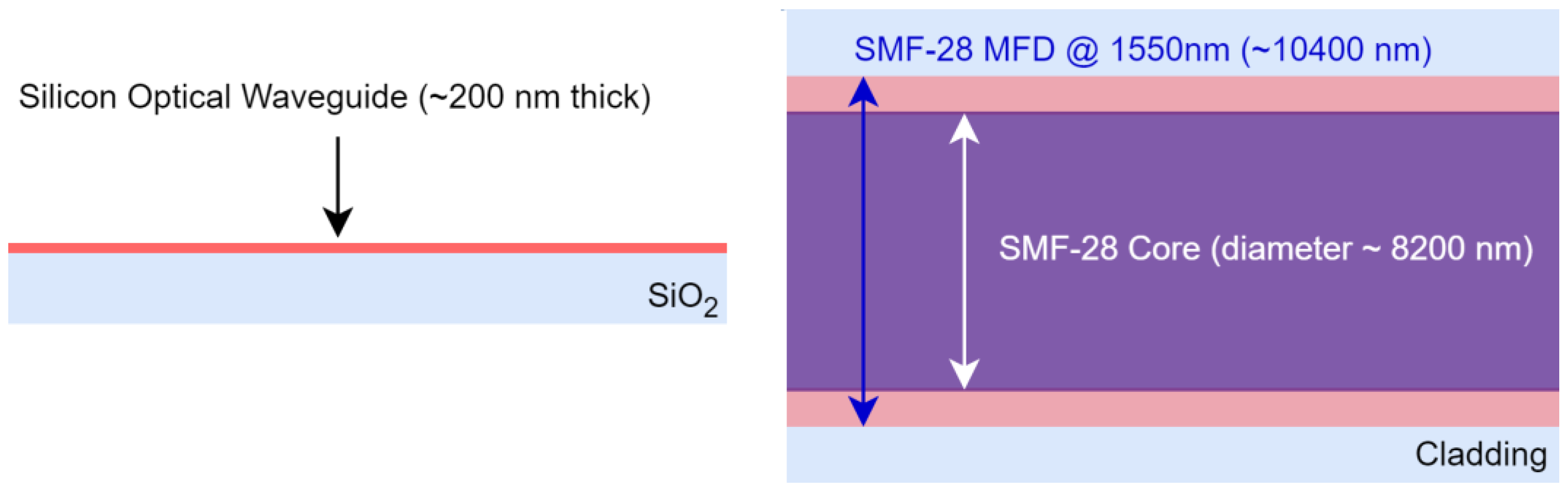
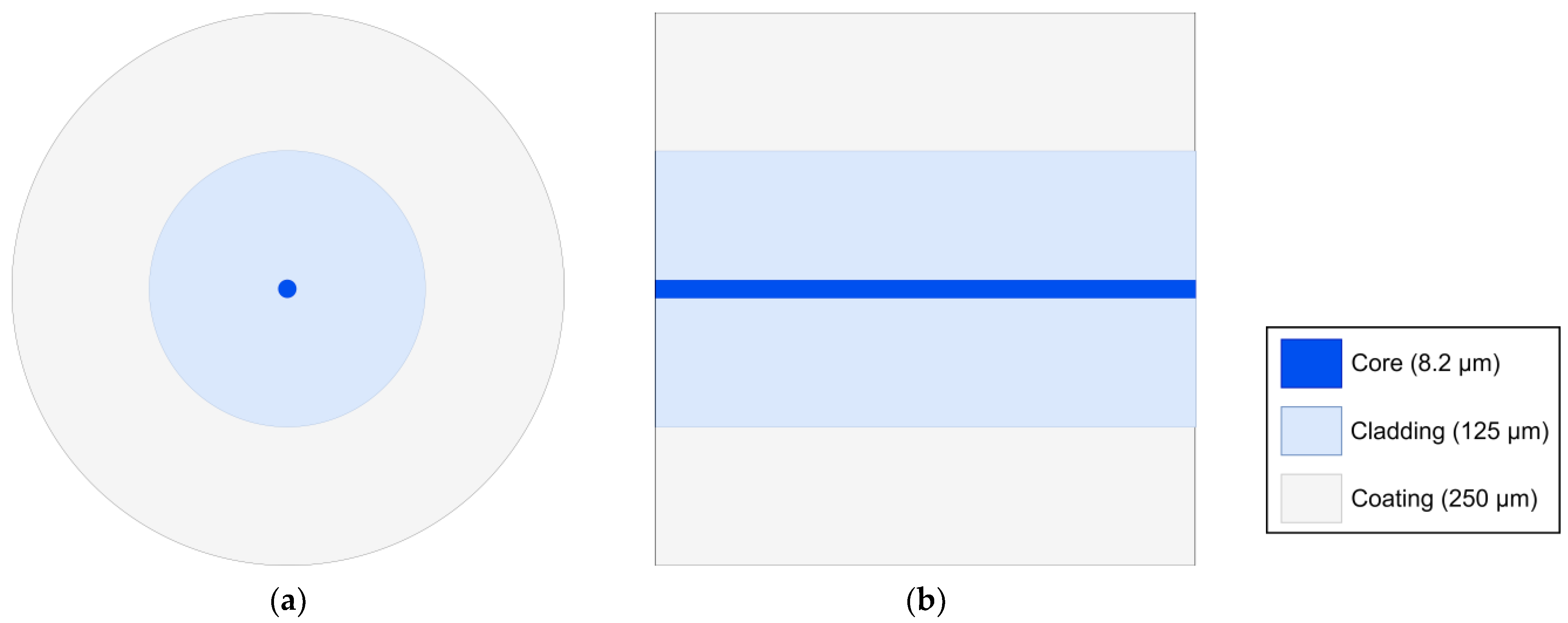
3.1. Single-Mode Optical Fiber

Considering a design operating wavelength of 1550 nm for the waveguide and light coupler, it is necessary to consider the effects of the coupling optical fiber. The fiber of choice is the SMF-28, due to its ultra-low propagation loss in the optical C-band (1530–1565 nm) and also for its ubiquity, being a very common type of optical fiber employed in optical communications, Figure 4.
A summary of the typical optical fiber parameters at a wavelength of 1550 nm is presented in Table 1. Since the refractive index of the optical fiber’s core and refractive index difference are known, it is possible to determine the average cladding refractive index, which is about 1.4629. The refractive index values are similar to the figures presented by Saktioto et al. for an SMF28e optical fiber [61].

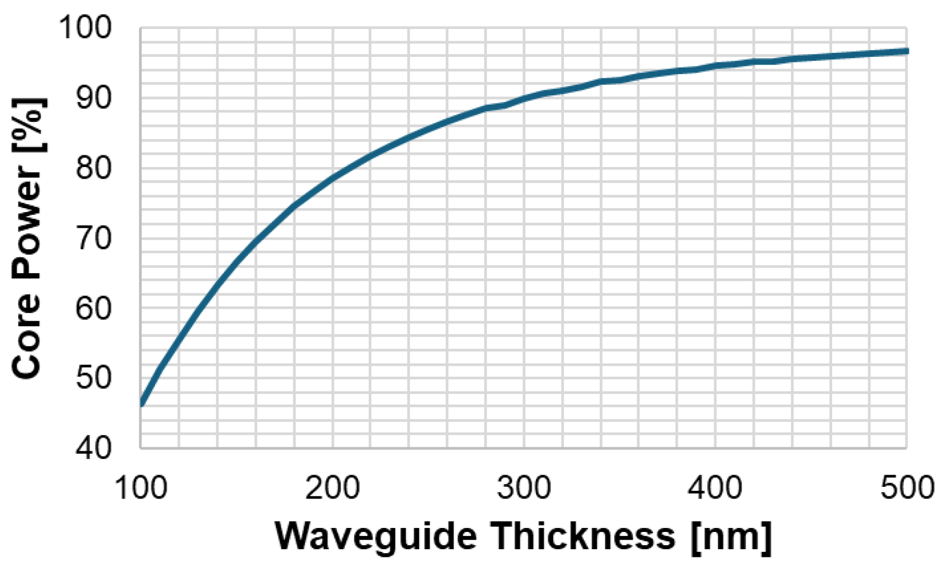
3.2. Single-Mode Waveguide

A 220 nm-thick hydrogenated amorphous silicon (a-Si:H) strip waveguide is used to couple light into the diffraction grating coupler. The model of the photonic waveguide material is the GUTL (Gauss–Urbach–Tauc–Lorentz) [63], which is based on the optical characteristics of a-Si:H. The complex refractive index at the operating wavelength (1550 nm) is approximately 3.4824 + 3.023 i × 10 8 .
The 220 nm a-Si:H layer is deposited over silica, and the environment is air, Figure 5. Attenuation was not calculated, as it depends on the width of the waveguide, and simulations were performed using a 2D model.

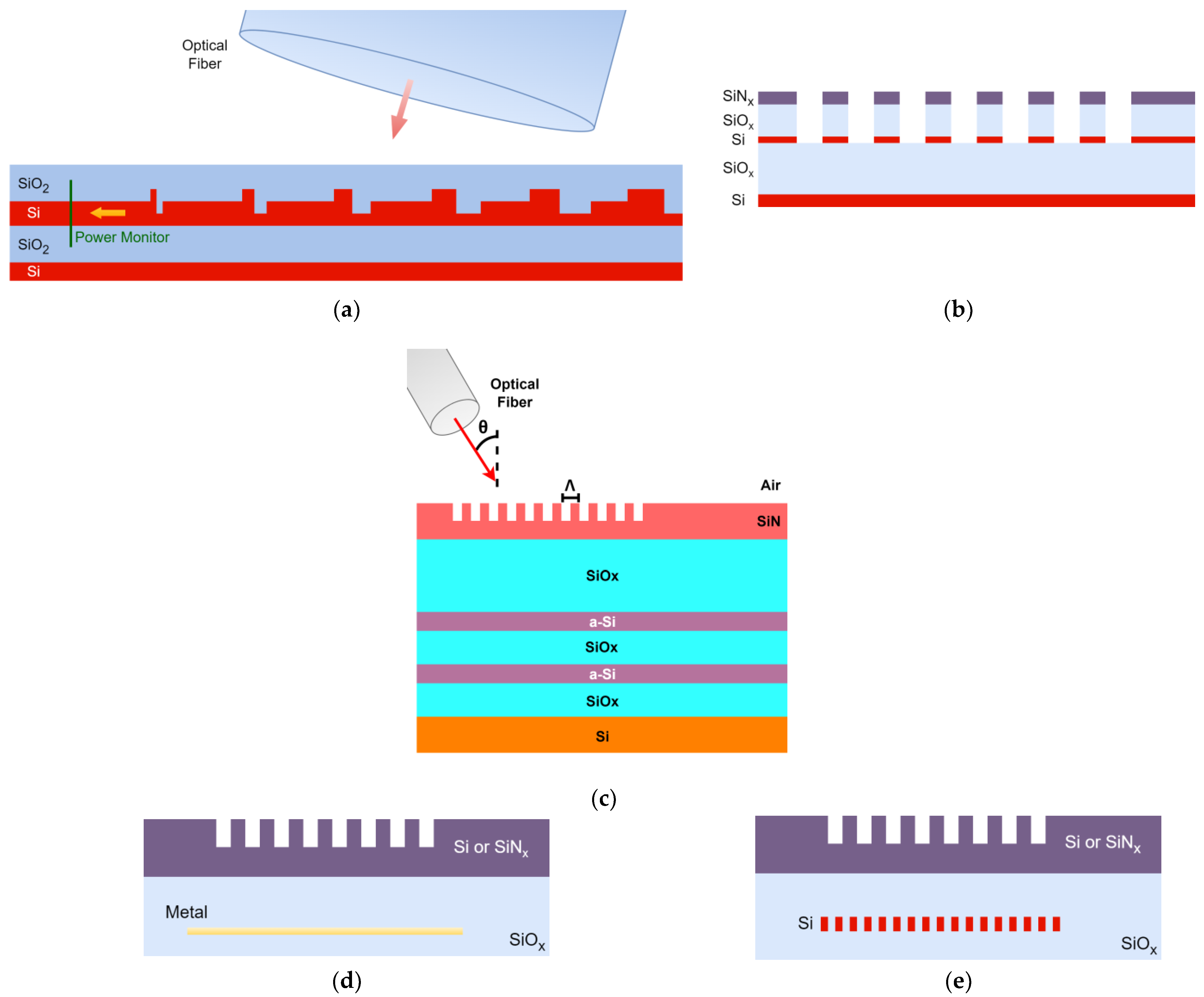
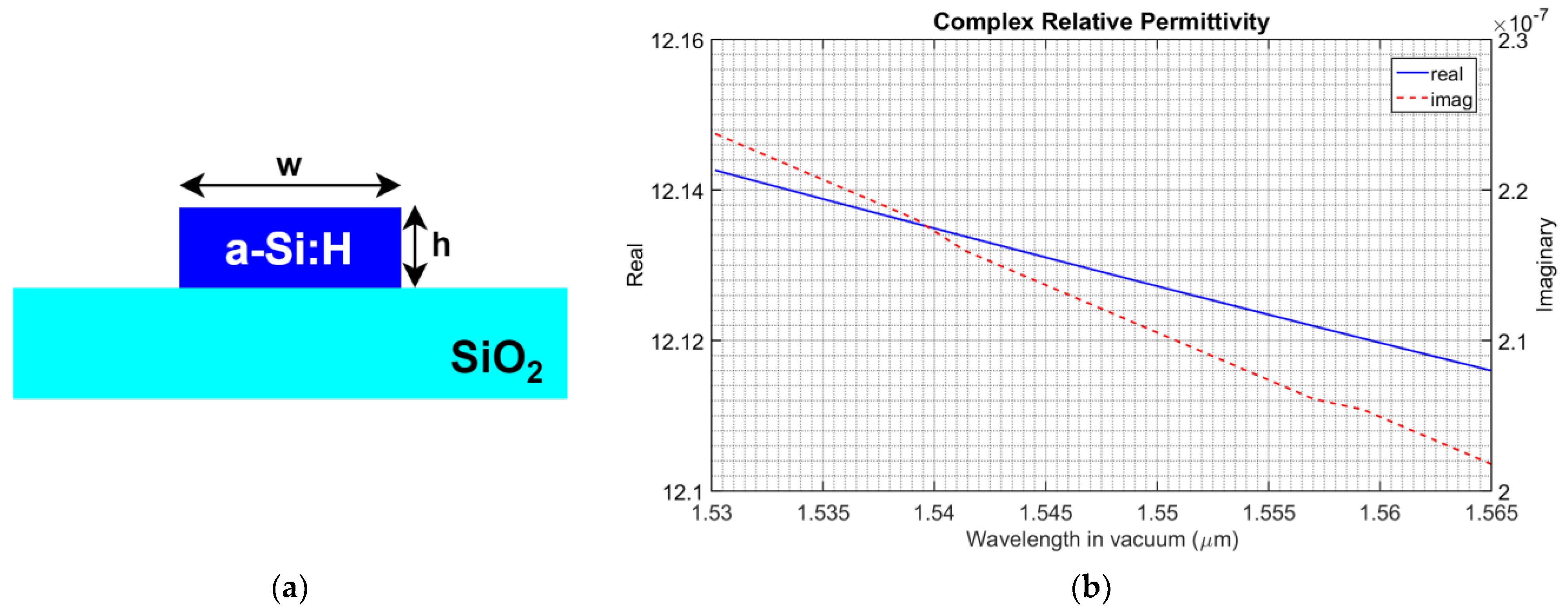
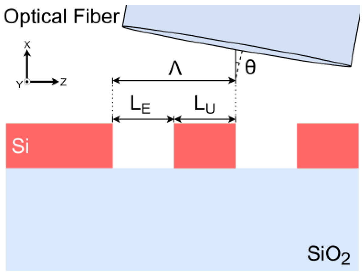
3.3. Grating Coupler Design

The main design parameters of a grating coupler are period ( Λ ), coupling angle ( θ ) and fill factor ( F ), Figure 6. A grating coupler can have a constant effective refractive index (fill factor and period) throughout its length, in a non-apodized design, or have a variation of the effective refractive index (fill factor, period or both) over its span in an apodized variant.
The fill factor corresponds to the ratio of the unetched length ( L U ) to the grating period ( Λ ), which can be expressed as a percentage (1):
F = L U Λ .
The effective refractive index of a diffraction grating coupler ( n e f f ) can be obtained from its fill factor ( F ), the refractive index of the etched ( n E ) and unetched segments ( n U ) of the grating, as described in expression (2) [50]:
n e f f = F × n U + 1 F × n E ,
in this equation, n E corresponds to the refractive index of air and n U to the effective refractive index of the waveguide’s fundamental quasi-transverse electric (TE) mode of propagation. Having the effective refractive index, n e f f , it is possible to calculate the required grating-coupler period ( Λ ), for a given coupling angle (θ), typically represented in degrees and free-space wavelength ( λ 0 ) as described in Equation (3) [64]:
Λ = λ 0 n e f f sin θ ,
the resulting grating period has the same units as the free-space wavelength; both are typically represented in units of nanometer (nm).
Having the main design expressions, it is possible to begin the design of a grating coupler in its simplest form. By defining the fill factor ( F ) as 0.5 (50%), while trying to keep the value of the denominator of expression (3) as low as possible, to achieve a higher period and, consequently, a large feature size, these measures can significantly decrease production costs if successfully implemented. The grating’s refractive index, n e f f , cannot be varied without changing the materials composing the grating coupler, the waveguide’s height or width, the fill factor or etch depth, so this value is regarded as a constant. The coupling angle, θ , was set to a very high value of 22.5°. The operating wavelength is 1550 nm, a typical value used in optical fiber communications, situated close to the middle of the optical C-band. Since the grating is fully etched, without upper cladding, and simulated in an environment filled with air, n E can be assumed as 1; n U was obtained using the Finite Element Method (FEM), having a value of approximately 2.8372. The effective refractive index of the grating coupler can now be obtained from Equation (2), having a value of about 1.9186. In the presence of all variables, it is now possible to calculate the grating’s period ( Λ ), Equation (3), which is approximately 1009.2 nm (1.0092 µm), resulting in a feature size of about 505 nm, a value close to the required width of a silicon single-mode strip waveguide operating at 1550 nm [30,31]. A grating coupler with these characteristics has a relatively narrow diffracted field. The grating coupler was simulated using the 2D-FDTD method and the coupling efficiency (SMF-28 optical fiber) measured under −9 dB. There was some discrepancy in the value of the coupling angle, which was found (in simulation) to be about 16.5° for optimum coupling. The values for coupling efficiency and coupling angle were obtained from the 2D-FDTD simulation tool (FullWAVE) provided with the RSoft software package (Synopsys, Inc., Sunnyvale, CA, USA). Comparing with uniform grating couplers reported in the literature [65,66], the simulated efficiency, −9.7 dB, is relatively low when contrasted with −7 dB [66] and −5.8 dB [65]. Since we are trying to maximize the feature size (in order to reduce production costs), the theoretical diffraction angle is also much higher, 22.5°, when compared to uniform grating coupler designs reported in the literature, of 8° [65] and 10° [66].

3.4. Grating-Coupler Optimization

Without apodization, grating couplers exhibit an exponential decay of the diffracted field over its length [55] (Figure 7a); due to this fact, most authors tend to prefer designs employing some form of apodization [39,40,51]. With this technique, the diffracted field distribution becomes more like a Gaussian throughout the grating coupler’s length [55], i.e., with the field distribution commonly found in optical fibers (Figure 7b) resulting in more efficient coupling.
In the most common approach, gratings feature linear apodization (i.e., the fill factor varies linearly throughout the grating’s length), Equation (4) [50].
F ( z ) = F 0 R × z ,
where F 0 corresponds to the grating’s initial fill factor (refer to expression (1)), R is the linear apodization factor, typically expressed in units of µm−1 or nm−1, and z corresponds to the distance from the beginning of the grating, usually in units of µm (if R is represented in µm−1) or nm (when R is represented in nm−1), respectively.

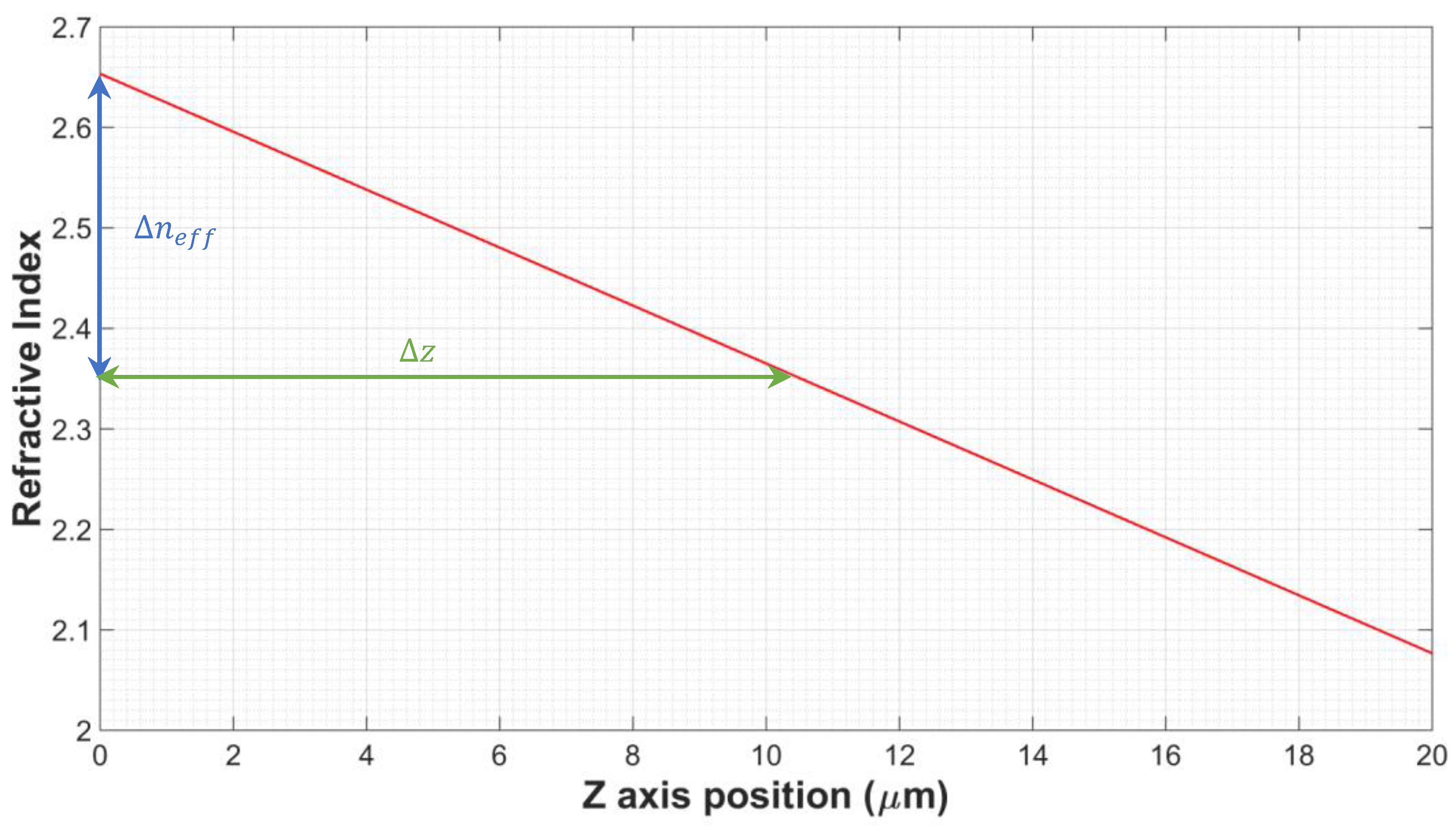
3.5. Linear Refractive-Index Variation

A linear variation of the grating’s refractive index can be achieved by varying both the period and fill factor over the grating coupler’s length, Figure 8, while maintaining the coupling angle constant.
The expression for the linear variation of the effective refractive index over a grating’s length can be written as (5)
n e f f z = n e f f 0 + m × z ,
where n e f f 0 is the effective refractive index at the start of the grating coupler (the effective refractive index of the first grating period), m corresponds to the slope of the refractive index variation, in µm−1, and z is the position measured from the start of the grating.
Following optimization in 2D-FDTD software, expression (6) was obtained for a 220 nm-thick fully etched grating coupler of hydrogenated amorphous silicon (a-Si:H), operating at a wavelength of 1550 nm:
n e f f z = 2.65348 0.0288 z .
The value of n e f f 0 , 2.65348, was obtained considering a maximum fill factor of 0.9 (90%), an etched-section refractive index, n E , of 1 and an unetched-section effective refractive index, n U , of 2.8372 (refer to expression (2)). The slope was adjusted considering a correlation which was observed between the length of the diffracted field distribution (Gaussian-like function) and the total variation of the refractive index over the grating coupler’s length. It was found on a 2D-FDTD simulation that for maximum coupling efficiency, the variation of the refractive index, n e f f , over a length of one optical fiber MFD (10.4 µm), z , had to be of about −0.3, resulting in a slope, m , of approximately −0.0288 µm−1. (Refer to expression (7) and plot of Figure 9.)
m = n e f f z   μ m 1 .
The plot of function (6) is represented in Figure 9, for a 20 µm grating coupler.
Accounting for the variation of the refractive index over the length of the grating coupler, it is possible to rearrange (2) to obtain the fill factor for each grating position (8):
F z = n e f f z n E n U n E .
The expression which gives the grating period (3) can also be rewritten to account for the variation of the effective refractive index over the grating’s length (9):
Λ z = λ 0 [ µ m ] n e f f ( z ) sin θ   [ µ m ] .
A computational algorithm, implemented in MATLAB (The MathWorks, Inc., LaGrange, GA, USA) obtains the effective refractive-index values at the begin of each grating period, using expression (6), and calculates the fill factor, F from function (8), and period, Λ, using expression (9) at each iteration, until the end of the grating coupler. The diffraction angle was defined as 15°. The pseudo-code algorithm is presented in Appendix A: this code sketch is used to represent the grating coupler in CAD, based on its geometric design parameters (fill factor and period) for each grating-segment iteration. The resulting grating coupler is presented in Figure 10. The length can overshoot the predefined value; in this case, for example, it is approximately 20.6 µm, instead of 20 µm. It was decided that it is preferable to have a slightly longer grating coupler than the opposite.
The fill factor (F) and period (Λ) for each grating segment, numbered from the beginning to the end of the grating coupler (or from left to right in Figure 10), considering a total of 28 segments, are presented in Table 2.

3.6. Quadratic Refractive-Index Variation

The refractive index of the grating coupler can also have a quadratic variation; in this case, the function which gives the refractive index over the grating’s length is defined as follows (10):
n e f f z = n e f f 0 + a × z 2 + b × z ,
following the same approach as in the previous subchapter, the initial fill factor, if defined as 0.9, results in an n e f f 0 of 2.65348, z corresponds to the grating position relative to its starting point, and a and b are the coefficients of the quadratic polynomial, with units µm−2 and µm−1, respectively. As in the linear function, a n e f f of −0.3 is pretended for a ∆z of 10.4 µm (measured from the grating’s starting point, z = 0). The vertex of the parabola is set to occur at or near the end of the grating coupler, at z m a x , 20 µm. With known values for n e f f (−0.3), ∆z (10.4 µm) and z m a x (20 µm), it is possible to calculate the values of the coefficients a and b , recurring to a system of linear equations (11):
n e f f = n e f f z n e f f 0 b 2 a = z m a x ,
which can be rearranged as (12)
n e f f = a × z 2 + b × z b 2 a = z m a x .
By solving the linear system, the values obtained for a and b are of approximately 9.745 × 10 4   μ m 2 and 3.898 × 10 2 μ m 1 , respectively. Equation (10) can now be rewritten with the approximated values of the quadratic function coefficients, which were rounded to the 3rd decimal place (13):
n e f f z = 2.65348 + 0.001 z 2 0.039 z .
The plot of the quadratic function which gives the effective refractive index for each position along the grating’s length is represented in Figure 11.
As in the linear variation of the refractive index, a computational algorithm was written in MATLAB (The MathWorks, Inc., LaGrange, GA, USA), to calculate the fill factor and period for each segment of the grating coupler, using expressions (8), (9) and (13). The pseudo-code is presented in Appendix B, this code sketch is used to represent the grating coupler in CAD based on its geometric design parameters (fill factor and period) for each grating-segment iteration. The grating coupler of Figure 12 was obtained after running the algorithm. As in the case of the grating coupler designed for linear refractive-index variation, the length of the grating slightly overshoots the preset value of 20 µm, achieving a length of about 20.25 µm over 28 periods (segments).
The period (Λ) and fill factor (F) of the quadratic refractive-index variation grating coupler is presented in Table 3, for a total of 28 segments.

3.7. Fill Factor Greater than 50%

An alternative to apodization is to use a fill factor different to 0.5 (50%); the fill factor was increased by over ½ in an attempt to decrease the decay rate of the diffracted-field intensity over the grating coupler’s length. In our observations of simulations using the 2D-FDTD method, there was evidence that a correlation exists between the fill factor and the exponential decay of the diffracted field. The higher the fill factor, the slower the decrease in the field over the grating’s length; however, there is also a drawback, since the field intensity (per unit area) decreases as the fill factor increases. The best result of our optimization process was obtained for a grating coupler with a period of 690 nm and a fill factor of approximately 82.6%, with a coupling angle (θ) of about 13.3°, Figure 13.

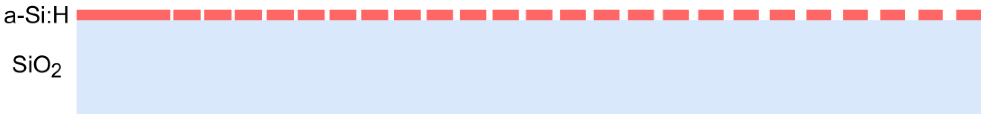
3.8. Overlapped-Grating Design

Another interesting method consists in the superposition (overlap) of two grating couplers with a fill factor of 0.5 (50%); using this method, it is possible to fabricate gratings using two lithography processes (and/or masks). This method enables the fabrication of grating couplers with fill factors different from ½, from designs with periods over 1000 nm, allowing the usage of masks with larger feature sizes and consequently lowering production costs. The coupling efficiency which results from this technique achieves values over −8 dB, as found in 2D-FDTD simulations (FullWAVE) performed with the RSoft software package (Synopsys, Inc., Sunnyvale, CA, USA) (refer to Section 4.7 and Section 5). The coupling efficiency obtained with this technique, −7.5 dB, is more similar to the value reported by Laere et al. [66], of −7 dB.
During the optimization process, the highest coupling efficiency (considering an SMF-28 optical fiber), was obtained for the overlap of two 1500 nm-period diffraction gratings, with a −400 nm z axis offset, Figure 14, resulting in a fill factor of 0.7(6) and an optimum coupling angle of 22°. The minimum feature size is 750 nm. The same grating coupler, if fabricated using a single lithography procedure, would have a feature size of 350 nm, requiring higher precision in mask fabrication.

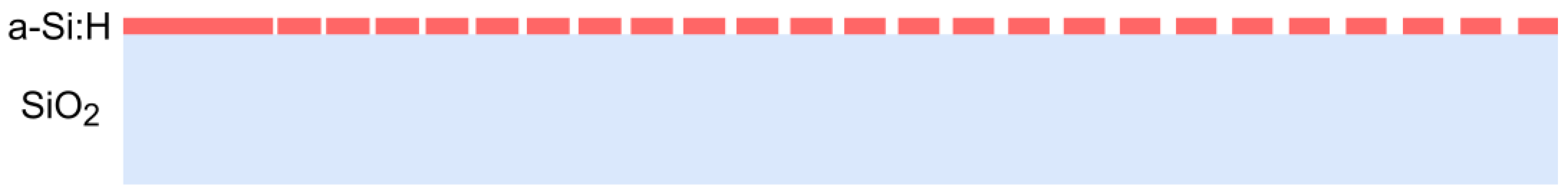
3.9. Random-Distribution Overlapped Grating Design

Following a similar approach as in the previous subchapter, overlapped grating couplers with chaotic (random) distribution were also simulated. To decrease production costs, the period of the gratings was set between 1 µm and 1.5 µm, and varied by steps of 0.1 µm. The combination which results in the highest efficiency consists in the overlap of 1.3 µm over a 1.5 µm grating, with a z-axis offset of −0.3 µm applied to the grating with the smallest feature size, Figure 15. For simplification purposes, both gratings have a fill factor of 0.5 (50%). The optimized coupling angle is about 20.9°.

4. Results

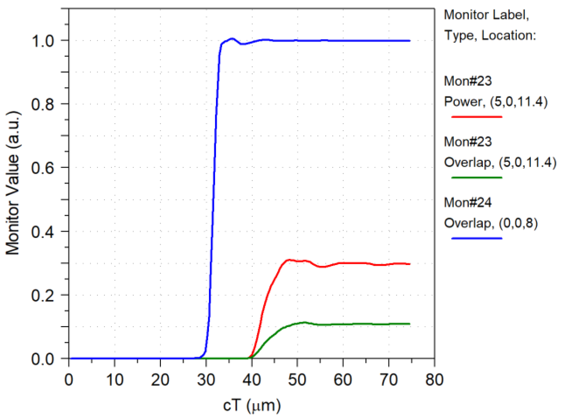
4.1. Fundamental Mode of the Waveguide

All grating couplers covered in this work are optimized for the fundamental quasi-transverse electric mode (quasi-TE00). The fundamental mode of the 220 nm-strip waveguide was analyzed using the 2D-FEM (two-dimensional finite element method). The effective refractive index of the quasi-TE00 mode of the waveguide is approximately 2.8372 , with an extinction coefficient of 3.037 × 10 8 for a 1550 nm operating wavelength. The intensity of the electric (Ey) and magnetic (Hx) major fields along the x axis is represented in Figure 16a and Figure 16b, respectively.
Variation of waveguide light confinement was simulated in 2D-FDTD for the quasi-TE00 mode for different thickness values of the a-Si:H layer thickness (height), considering an operating wavelength in vacuum of 1550 nm. With a 220 nm-thick layer, approximately 81.8% of the total waveguide power is inside the a-Si:H core. The waveguide light confinement follows a logarithmic-like distribution, Figure 17; lower a-Si:H thickness values result in more power being transferred to the substrate and cover (air), while the opposite is verified for high thickness values, where most of the launch power is carried in the waveguide’s core. Sensing applications typically explore the evanescent field effect, and in such cases, a tradeoff must be made between power loss and light confinement.

4.2. Simulated Single-Mode-Fiber Fundamental Mode

To estimate the coupling efficiency, it is necessary to obtain the field distribution for the typical parameters of the single-mode optical fiber (SMF-28) of the coupling setup (refer to Table 1). The optical fiber was simulated using 2D-FDTD, like the single-mode waveguide. The CAD design is identical to that presented in Figure 4b; for simplicity and algorithm-efficiency reasons, the effects of the coating layer were not considered. The results of the simulation of the fiber model are presented in Figure 18, showing the electric, Ey (a) and magnetic, Hx (b) field distributions along the x axis, for the TE00 mode, at a wavelength of 1550 nm.

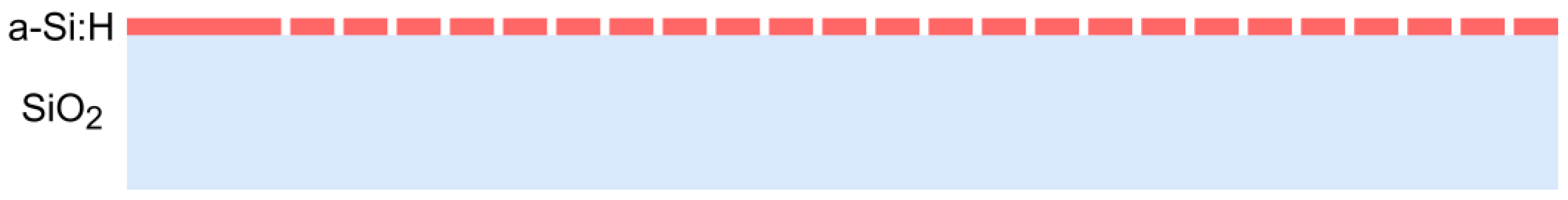
4.3. Non-Optimized Grating-Coupler Performance

As previously mentioned, without apodization and with a fill factor of 0.5 (50%), the coupling efficiency is typically modest. In the simulation that we performed, a value slightly above −10 dB was obtained for this parameter. It is thought to be of imperative importance that some additional measures are taken to improve grating-coupler performance.
Two monitors were used in the calculation of coupling efficiency, one centered at position (x, z) = (0, 8), measuring the power near the output of the waveguide, and another centered at position (x, z) = (5, 11.4), to measure the overlap between the diffracted field and the fundamental mode of the optical fiber. This second monitor is placed at an angle of 16.5° (optimized coupling angle): its center is at a distance of 5 µm from the grating center axis and at a distance of 2.4 µm from the grating coupler’s starting point, measured on the vertical z axis. The access waveguide is 9 µm long.
In Figure 19, it is noticeable that the diffracted electric-field intensity decays at a very high rate (exponentially), following the two first periods of the grating coupler; due to this fact, coupling efficiency, Figure 20, is relatively low. In Figure 20, and in subsequent figures, the abscissa label “cT” corresponds to a time-related unit, which is given as the product of the velocity of light in vacuum ( c ) and time ( τ ). Since the velocity of light is constant, this unit represents the space travelled by light for a given time interval, in units of micrometer (μm).
Looking at the results presented in Figure 20, it is possible to assert that the waveguide-monitor overlap (with the launch field, or fundamental quasi-TE00 mode) remains nearly constant throughout the integration time. The coupling-efficiency value achieved at the time of convergence is slightly over −9.7 dB (~10.8%). The overlap with the diffracted field (i.e., the percentage of power of the diffracted field passing through the monitor which is converted to the SMF-28 fundamental mode) is about 36.4%. The ratio of the diffracted power reaching the monitor to the waveguide’s power is slightly over −5.3 dB (~29.7%).

4.4. Constant Refractive Index and Fill Factor Greater than 50%

The results of the grating coupler featuring an 82% fill factor and a period of 690 nm are presented herein. In Figure 21, the contour map of the diffracted electric field is presented. Two monitors are included, one centered at position (x, z) = (0, 5), measuring the power near the output of the waveguide, and another centered at position (x, z) = (4, 11.2), which measures the overlap between the diffracted field and the fundamental mode of the optical fiber. This second monitor is placed at an angle of 13.3° (optimized coupling angle); its center is at a distance of 4 µm from the grating center axis and at a distance of 5.2 µm, measured from the grating coupler’s starting point. The access waveguide is 6 µm long.
In Figure 21, it is possible to notice that the diffracted field intensity decays (exponentially) along the coupler’s length, a characteristic of non-apodized grating couplers. By optimizing the fill factor, monitor angle and position, it was possible to maximize the coupling efficiency.
Efficiency test results are shown in Figure 22. It is possible to verify that the waveguide-monitor overlap (with the launch field, or fundamental quasi-TE00 mode) remains nearly constant throughout the integration time. The coupling-efficiency value achieved at the time of convergence is slightly under −4.3 dB (~36.9%). The overlap with the diffracted field (i.e., the percentage of power of the diffracted field passing through the monitor which is used to excite the SMF-28 fundamental mode) is about 85.6%. The ratio of the diffracted power reaching the monitor to the waveguide’s power is slightly over −3.7 dB (~43.1%).
Coupling efficiency was measured for wavelengths in vacuum between 1520 nm and 1580 nm, Figure 23. The −1 dB bandwidth is about 25 nm and the −3 dB bandwidth is 44 nm. The center wavelength (peak efficiency) occurs at 1549 nm. The optical C-band (1530–1565 nm) is covered with a maximum 2 dB penalty.

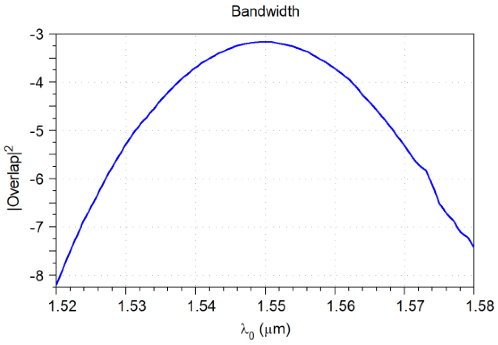
4.5. Linear Effective-Refractive-Index Variation

The results of the apodized grating coupler with linear variation of the effective refractive index are presented herein. In Figure 24, the distribution of the diffracted electric field is shown. Two monitors are included, one centered at position (x, z) = (0, 6), measuring the power near the output of the waveguide, and another centered at position (x, z) = (4, 13.3), measuring the overlap between the diffracted field and the fundamental mode of the optical fiber. The second monitor is positioned at an angle of 10.8° (optimized coupling angle); its central position is at a distance of 4 µm from the grating-center axis relative to the x axis and at a distance of 6.3 µm, measured from the grating coupler’s starting point on the z axis. The access waveguide is 7 µm long.
In Figure 24, it can be noticed that the diffracted field intensity has a distribution closer to a Gaussian, having a higher intensity near the center of the monitor, a characteristic of apodized designs. By optimizing apodization, monitor angle and position, it was possible to maximize coupling efficiency. The values of period and fill factor presented in Table 2 were limited to two decimal points in simulations, since most optical lithography systems do not have precisions greater than 10 nm. The impact of this loss of precision in the simulation results was found to be minimal.
In Figure 25, efficiency results are presented. It is possible to confirm that the waveguide monitor overlap (with the launch field, or fundamental quasi-TE00 mode) remains nearly constant throughout the integration time. The coupling efficiency achieved at the time of convergence is slightly under −3.1 dB (~48.4%). The overlap with the diffracted field (i.e., the percentage of power of the diffracted field passing through the monitor which is used to excite the SMF-28 fundamental mode) is approximately 96.1%. The ratio of the diffracted power reaching the monitor to the waveguide’s power is slightly over −3 dB (~ 50.4%).
Coupling efficiency was measured for wavelengths in vacuum between 1520 nm and 1580 nm, Figure 26. The −1 dB bandwidth is approximately 26 nm, and the −3 dB bandwidth is 47 nm. Peak efficiency (center wavelength) occurs at 1550 nm. The optical C-band (1530–1565 nm) is covered with a maximum 2.1 dB penalty.

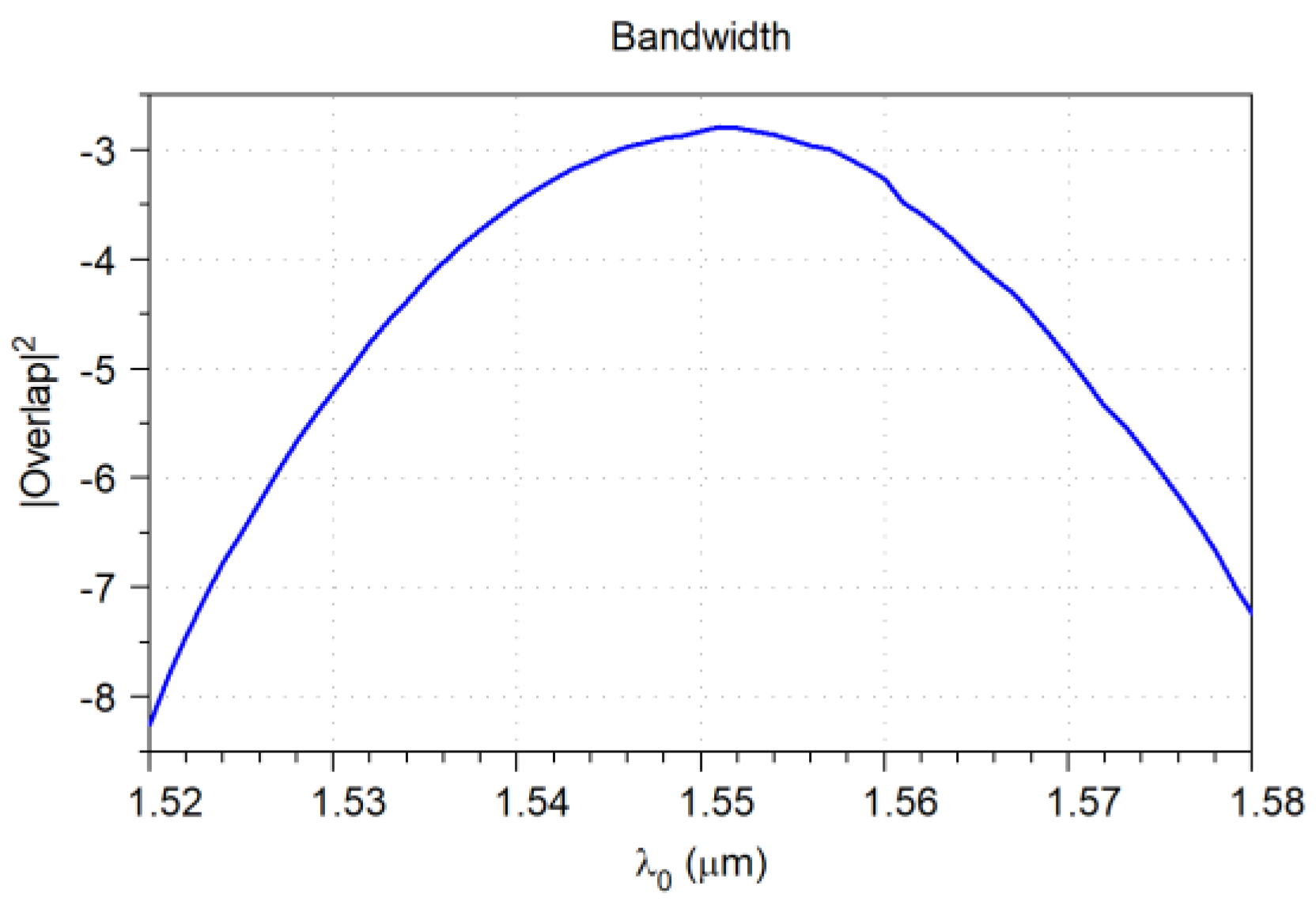
4.6. Quadratic Effective-Refractive-Index Variation

The performance results of the apodized grating coupler with quadratic (polynomial) variation of the effective refractive index are presented in this subchapter. In Figure 27, the distribution of the diffracted electric field is shown. Two monitors are included, one centered at position (x, z) = (0, 6), measuring the power near the output of the waveguide, and another centered at position (x, z) = (4, 12.9), measuring the overlap between the diffracted field and the fundamental mode of the optical fiber. The second monitor is positioned at an angle of 10.5° (optimized coupling angle); its center is at a distance of 4 µm from the grating center axis, relative to the x axis, and at a distance of 5.9 µm, measured from the grating coupler’s starting point, on the z axis. The waveguide has a length of 7 µm.
After looking carefully at Figure 27, it can be noticed that the diffracted field intensity has a Gaussian-like distribution, as in the previous apodized grating coupler, exhibiting higher intensity near the center of the monitor, a characteristic of apodized designs. By optimizing apodization, monitor angle and position, it was possible to maximize the coupling efficiency. The values of period and fill factor presented in Table 3 were limited to two decimal points in simulations, due to the fact that most optical lithography systems do not have precisions greater than 10 nm. The impact of this loss of precision was verified as having a negligible impact on the results.
In Figure 28, coupling efficiency results are depicted. It is possible to verify that the waveguide monitor overlap (with the launch field, or fundamental quasi-TE00 mode), remains nearly constant throughout the integration time. Coupling efficiency achieved at the time of convergence is slightly under −2.8 dB (~52.2%). The overlap with the diffracted field (i.e., the percentage of power of the diffracted field passing through the monitor which is used to excite the SMF-28 fundamental mode) is around 97.4%. The ratio of the diffracted power reaching the monitor to the waveguide’s power is slightly under −2.7 dB (~53.6%).
Coupling efficiency was measured for wavelengths in vacuum between 1520 nm and 1580 nm, Figure 29. The −1 dB bandwidth is approximately 25 nm and the −3 dB bandwidth is 46 nm. Peak efficiency (center wavelength) occurs at 1551 nm. The optical C-band (1530–1565 nm) is covered with a maximum 2.4 dB penalty.

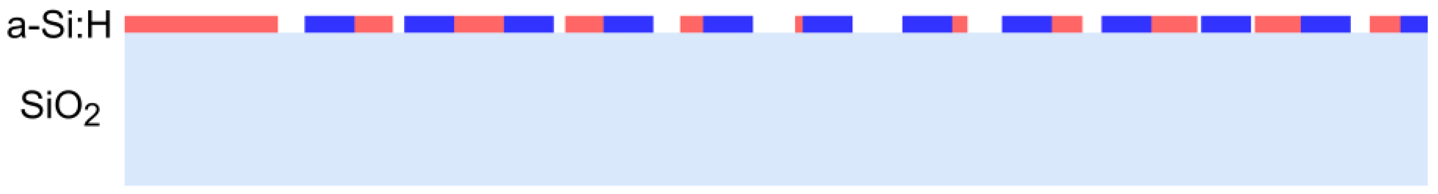
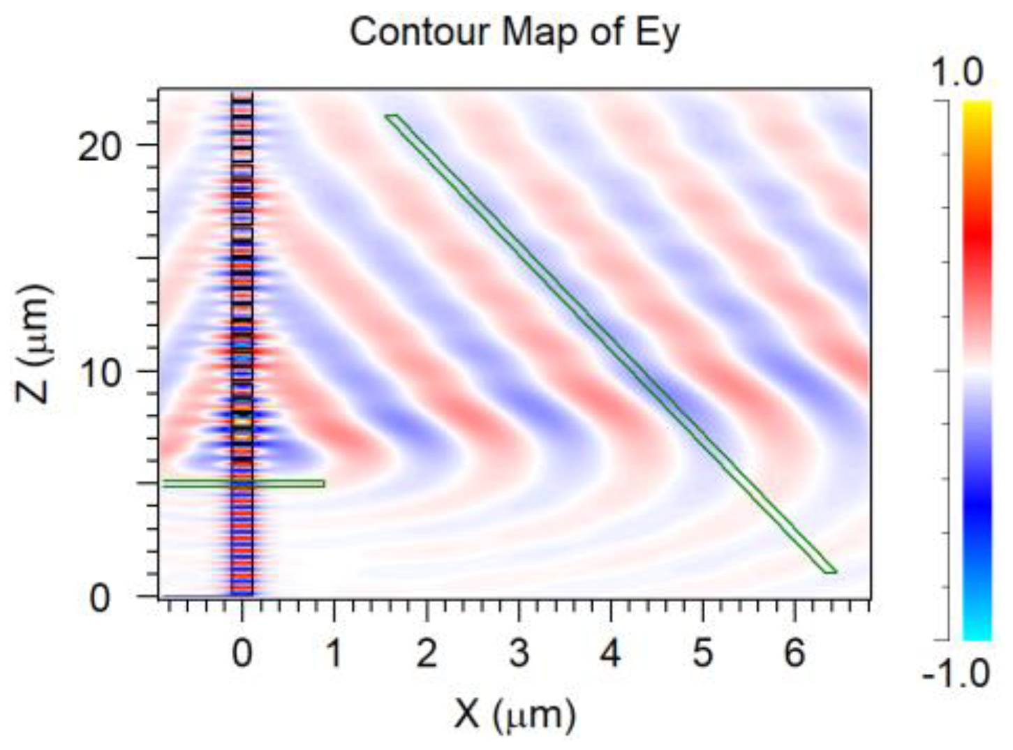
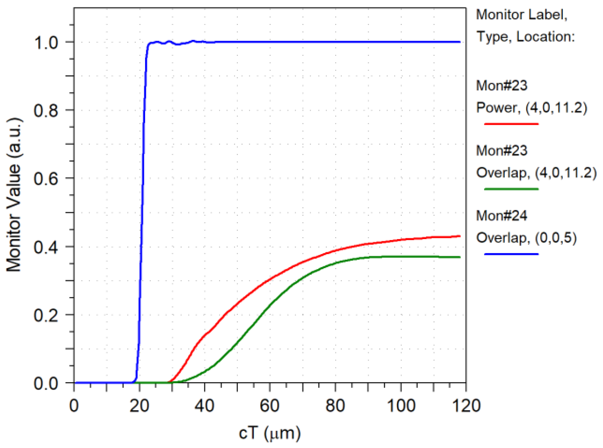
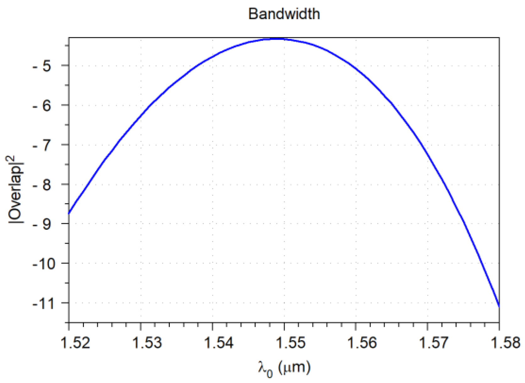
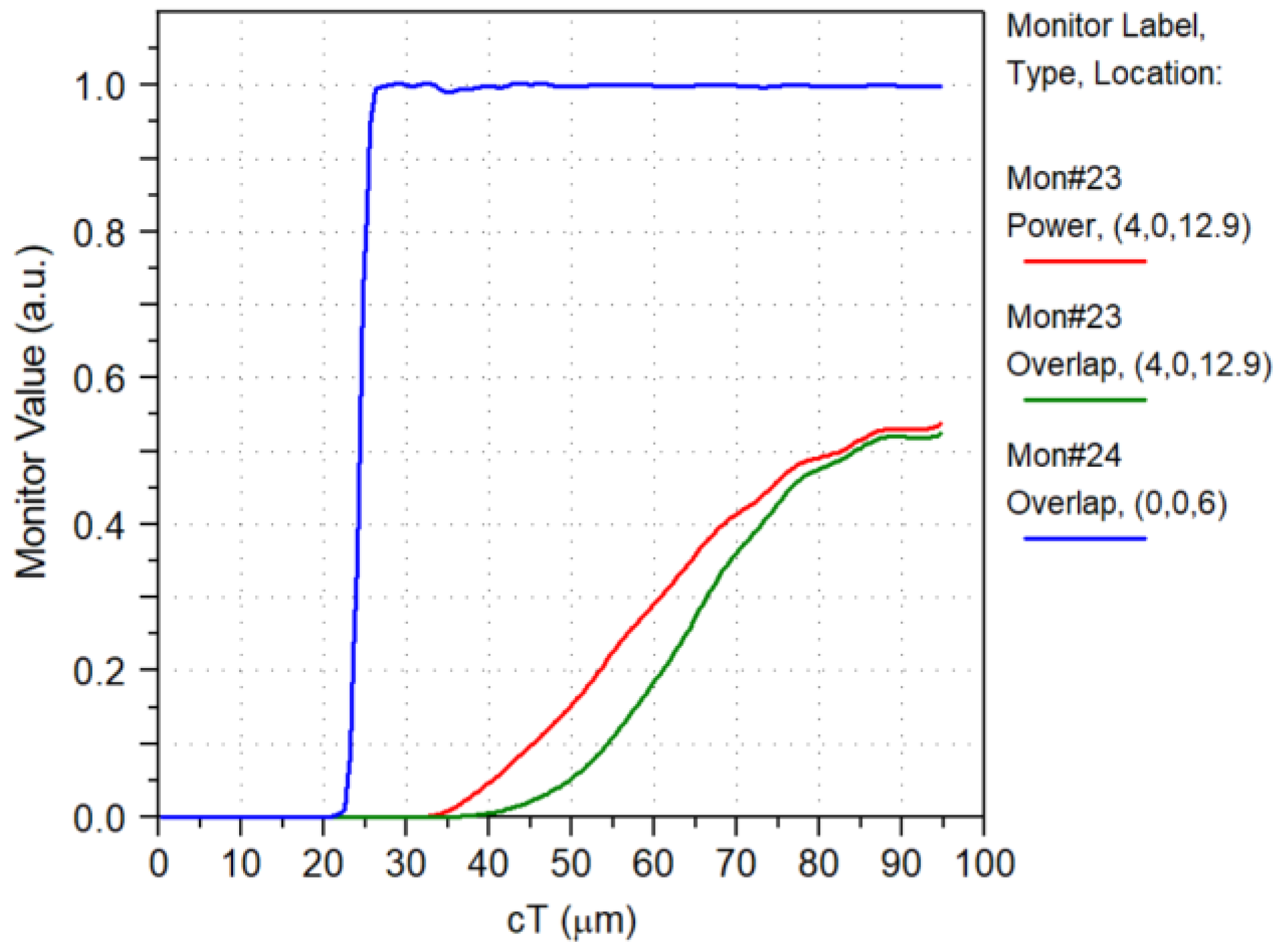
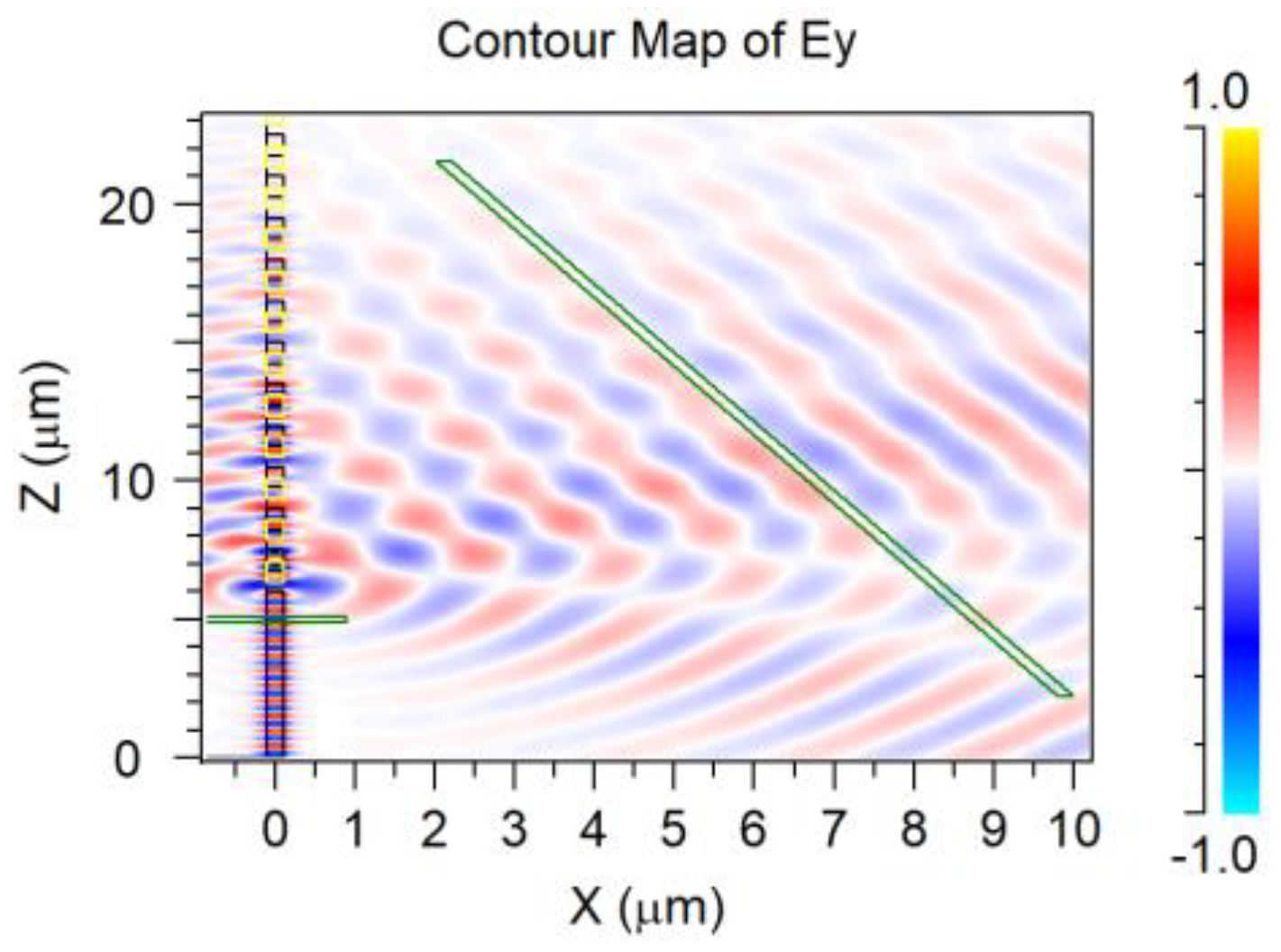
4.7. Overlapped Micrometric Design

The coupling efficiency results for the overlapped micrometric period gratings (1500 nm) are presented herein. The two superimposed gratings with an offset of −400 nm form a grating coupler with a period of 1500 nm and a fill factor of 0.7(6) (76(6)%). In Figure 30, the contour map of the diffracted electric field is presented.
Two monitors are included, one centered at position (x, z) = (0, 5), measuring the power near the output of the waveguide, and another centered at position (x, z) = (6, 11.9), which measures the overlap between the diffracted field and the fundamental mode of the optical fiber. This second monitor is placed at an angle of 22° (optimized coupling angle); its center is at a distance of 6 µm from the grating center axis (due to the higher coupling angle) and at a distance of 5.9 µm, measured from the grating coupler’s starting point. The access waveguide is 6 µm long.
In Figure 30, it is possible to notice that the diffracted field intensity (exponentially) decays along the coupler’s length, a characteristic of non-apodized grating couplers. By optimizing the fill factor, monitor angle and position, it was possible to maximize the coupling efficiency.
In Figure 31, coupling efficiency results are shown. It is possible to attest that the waveguide-monitor overlap (with the launch field, or fundamental quasi-TE00 mode), remains nearly constant throughout the integration time. Coupling efficiency achieved at the time of convergence is slightly over −7.5 dB (~20.0%). The overlap with the diffracted field (i.e., the percentage of power of the diffracted field passing through the monitor which is used to excite the SMF-28 fundamental mode) is approximately 80.8%. The ratio of the diffracted power reaching the monitor to the waveguide’s power is slightly under −6.5 dB (~22.3%).
Coupling efficiency was measured for wavelengths in vacuum between 1530 nm and 1565 nm, Figure 32. The −1 dB bandwidth is approximately 22 nm. Peak efficiency (center wavelength) occurs at 1549 nm. The optical C-band (1530–1565 nm) is covered with a maximum 6.3 dB penalty.

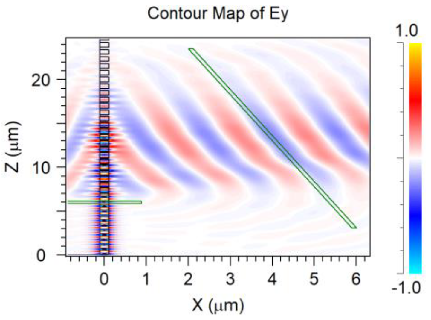
4.8. Random Distribution

Results obtained for the random (chaotic)-distribution grating coupler are presented in this subchapter. Two gratings with periods of 1500 and 1300 nm were overlapped, with the second grating having a z axis offset of −300 nm. This was the combination which held the best results for a grating coupler featuring a random distribution, achieved by the superposition of two gratings with periods over 1000 nm.
Two monitors are included, one centered at position (x, z) = (0, 6), measuring the power near the output of the waveguide, and another centered at position (x, z) = (6, 11.4), which measures the overlap between the diffracted field and the fundamental mode of the optical fiber. This second monitor is placed at an angle of 20.9° (the optimized coupling angle); its center is at a distance of 6 µm from the grating center axis (due to the higher coupling angle) and at a distance of 4.4 µm, measured from the grating coupler’s starting point. The waveguide is 7 µm long.
In Figure 33, it is noticeable that the diffracted electric field shows several diffraction angles, resulting in a poor coupling efficiency, Figure 34.
Looking at the results presented in Figure 34, it is possible to assert that the waveguide-monitor overlap (with the launch field, or fundamental quasi-TE00 mode), remains nearly constant throughout the integration time. The coupling-efficiency value achieved at the time of convergence is slightly under −12.8 dB (~5.2%). The overlap with the diffracted field (i.e., the percentage of power of the diffracted field passing through the monitor which is converted into the SMF-28 fundamental mode) is about 33.3%. The ratio of diffracted power reaching the monitor to the waveguide’s power is slightly over 8.1 dB (~15.7%).

5. Discussion

To summarize, all results obtained in this work are presented and compared with state-of-the-art (SoA) and high-efficiency grating-coupler designs, Table 4. All grating couplers presented herein were projected to operate in the optical C-band (1530–1565 nm), and the coupling efficiency of the proposed designs is given for a wavelength of 1550 nm. In Table 4, GC stands for grating coupler, N/A means information is not available, BW corresponds to bandwidth and DBR is distributed Bragg reflector.
Despite having inferior performance when compared to the state of the art in grating-coupler designs, the proposed GCs have the possibility of being manufactured at a lower cost. The devices, made of a-Si:H, can be deposited at low temperature by Plasma-Enhanced Chemical Vapor Deposition (PECVD), over a substrate of silica. Since silica is one of the main constituents of glass, there is also the possibility of adapting the devices to be fabricated over a substrate of this material.
Due to the fully etched grating design, all devices can be fabricated using one or two lithographic masks, making misalignment less of an issue. Designs requiring three lithographic processes are more affected by misalignment issues, and a study about the impact of misalignment must be conducted [40]. Using the method covered in this work, no silicon wafers are required, and the devices work without any bottom silicon layer(s) or upper cladding. Without a bottom reflector layer, the proposed grating couplers were designed to shape the diffracted field to enhance the overlap with the coupling profile of the single-mode optical fiber. The fill factor (and period, in apodized designs) was engineered to achieve the intended diffracted-field distribution. All presented designs can be patterned by photolithography [68], requiring either deep-UV (DUV) or extreme-UV (EUV) lithographic processes.
Regarding the performance of the presented devices, it is clear that apodization plays a significant role in performance enhancement, at the cost of requiring more expensive lithographic procedures, such as DUV, EUV or E-beam. The results suggest that quadratic refractive-index variation might present a small improvement in coupling efficiency when compared with linear variation. By optimizing the fill factor or opting for a grating made from the overlap of two lithographic masks, it is possible to make a compromise between performance and manufacturing costs. We were unable to achieve acceptable results from pseudo-random distributions; nevertheless, these could be the basis for more sophisticated optimization, such as, for example, genetic algorithms, by creating seed samples. In addition, it might be necessary to decrease the feature size of such grating designs, to improve efficiency.

6. Conclusions

Five different grating couplers were successfully designed and simulated, achieving coupling efficiencies between −12.8 dB and −2.8 dB. These results were obtained considering a hydrogenated amorphous silicon (a-Si:H) over silica platform, without any silicon bottom layer or bottom reflector. The technology is compatible with low-temperature PECVD and HWCVD, significantly reducing production costs.
Since the designs are fully etched, only one or two lithographic masks are required, reducing the dependency on mask alignment.
The simulations were conducted using the Finite-Difference Time-Domain (FDTD) analysis and Finite Element Method (FEM). The optical-fiber model was based on a commercial type (SMF-28), typically used in near-infrared communications, being characterized by typical design parameters.
The grating coupler featuring quadratic variation of the effective refractive index achieved the highest efficiency of the devices studied in this work (−2.8 dB), opening the way for studies of different arithmetic functions or combination of functions (e.g., polynomial, exponential, logarithmic, hyperbolic) in the variation of the refractive index through the grating’s length.
The superposition of two masks to produce a different grating coupler from two gratings is also a possible method, which allows a more complex design, with smaller feature sizes to be fabricated using photolithography techniques, thus avoiding electron beam (e-Beam).

7. Future Work and Improvement

From our perspective, this work contributes to open ways to future research in the optoelectronics and photonics fields, in which several paths undeniably still need to be explored. Since the analysis covered in this work was performed using a bidimensional model, further analysis should be conducted using a tridimensional (3D) model. With one more dimension, simulation of adiabatic tapers for grating coupler (GC) connection and focusing grating designs can be studied, and its geometry optimized. Following the tridimensional analysis, it is time to proceed to the production of real-world prototypes, followed by characterization and testing.
Despite the increase in costs and complexity, the inclusion of one or more bottom layers of silicon (arranged as a DBR stack) and under-cladding thickness adjustment could provide possibilities for further improvements in performance, opening the way fora performance comparison analysis of such designs, with the same GC devices featuring metal bottom reflectors.
It is also important to study the impacts of the arithmetic functions used in the apodization of the grating couplers to tailor the shape, distribution and length of the diffracted field, and to analyze its importance in matching the optical fiber’s field profile and mean field diameter (MFD). In addition, it is relevant to study the effects on the diffracted field, of the slope and initial fill factor in linear apodization and of the coefficients of polynomial functions, like the quadratic distribution (where concavity can play a significant role).
Of course, there is also space for the utilization of machine learning (e.g., neural networks) and other artificial intelligence techniques for the optimization of apodization parameters. The study of arithmetic functions alone or combined opens an interesting perspective in the optimization of diffraction grating couplers.

Author Contributions

Conceptualization, D.A., J.C. and A.F.; methodology, D.A., J.C. and A.F.; software, D.A. and P.L.; validation, J.C. and A.F.; writing—original draft preparation, D.A.; writing—review and editing, J.C., A.F. and M.V.; supervision, J.C., A.F. and M.V.; project administration, A.F.; funding acquisition, A.F and M.V. All authors have read and agreed to the published version of the manuscript.

Funding

This research was supported by Portuguese national funds provided by FCT—Fundação para a Ciência e a Tecnologia, through grant SFRH/BD/07792/2021 (https://doi.org/10.54499/2021.07792.BD) and funded by the Portuguese FCT program, Center of Technology and Systems (CTS) UIDB/00066/2020/UIDP/00066/2020 and by FCT project ASER-META 2022.07694.PTDC.

Institutional Review Board Statement

Not applicable.

Informed Consent Statement

Not applicable.

Data Availability Statement

The datasets presented in this article are not readily available because the data are part of an ongoing study. Requests to access the datasets should be directed to [email protected] or [email protected].

Conflicts of Interest

The authors declare no conflicts of interest.

Appendix A

The pseudo-code algorithm employed to obtain the grating period (Λ) and fill factor (F), for each segment of grating coupler featuring linear refractive-index variation along its length, is presented herein:
gratingLength = 20;//micrometer
delta_neff = −0.3;//1/micrometer
delta_z = 10.4;//micrometer (SMF-28 MFD)
m = delta_neff/delta_z;
neff0 = 2.65348;//F = 0.9
theta = deg2rad(15);//15 deg
ne = 1;//air
nu = 2.8372;//220 nm aSiH strip waveguide (2D-FEM)
lambda0 = 1.55;//micrometer
 
z = 0;
neff = 0;
GP = 0;
F = 0;
num = 1;
 
while (z < gratingLength){
neff = m*z + neff0;
GP = lambda0/(neff − sin(theta));//GP = Grating period (micrometer)
F = (neff − ne)/(nu − ne);
 
print(“GP”+num2str(num)+” = “+num2str(GP,3)+“\r\n”);//round to nm
print(“F”+num2str(num)+” = “+num2str(F,3) + “\r\n”);//round to nm
z = z + GP;
num = num + 1;
}

Appendix B

The pseudo-code used to obtain the period (Λ) and fill factor (F), for each segment of the grating coupler, featuring quadratic variation of the refractive index through its length, is presented below:
a = 0.001;
b = −0.039;
gratingLength = 20;//micrometer
neff0 = 2.65348;//F = 0.9
theta = deg2rad(15);//15 deg
ne = 1;//air
nu = 2.8372;//220 nm aSiH strip waveguide (2D-FEM)
lambda0 = 1.55;//micrometer
 
z = 0;
neff = 0;
GP = 0;
F = 0;
num = 1;
 
while (z < gratingLength){
neff = a*z^2 + b*z + neff0;
GP = lambda0/(neff - sin(theta));//GP = Grating period (micrometer)
F = (neff - ne)/(nu - ne);
 
print([“GP”+num2str(num)+” = “+num2str(GP,3)+“\r\n”]);//round to nm
print([“F”+num2str(num)+” = “+num2str(F,3)+“\r\n”]);//round to nm
 
z = z + GP;
num = num + 1;
}

References

  1. Sengupta, K.; Nagatsuma, T.; Mittleman, D.M. Terahertz integrated electronic and hybrid electronic–photonic systems. Nat. Electron. 2018, 1, 622–635. [Google Scholar] [CrossRef]
  2. Thraskias, C.A.; Lallas, E.N.; Neumann, N.; Schares, L.; Offrein, B.J.; Henker, R.; Plettemeier, D.; Ellinger, F.; Leuthold, J.; Tomkos, I. Survey of photonic and plasmonic interconnect technologies for intra-datacenter and high-performance computing communications. IEEE Commun. Surv. Tutor. 2018, 20, 2758–2783. [Google Scholar] [CrossRef]
  3. Pelucchi, E.; Fagas, G.; Aharonovich, I.; Englund, D.; Figueroa, E.; Gong, Q.; Hannes, H.; Liu, J.; Lu, C.Y.; Matsuda, N.; et al. The potential and global outlook of integrated photonics for quantum technologies. Nat. Rev. Phys. 2022, 4, 194–208. [Google Scholar] [CrossRef]
  4. Lukin, D.M.; Guidry, M.A.; Vučković, J. Integrated Quantum Photonics with Silicon Carbide: Challenges and Prospects. PRX Quantum 2020, 1, 020102. [Google Scholar] [CrossRef]
  5. Pinske, J.; Teuber, L.; Scheel, S. Highly degenerate photonic waveguide structures for holonomic computation. Phys. Rev. A 2020, 101, 062314. [Google Scholar] [CrossRef]
  6. Huang, C.; Sorger, V.J.; Miscuglio, M.; Al-Qadasi, M.; Mukherjee, A.; Lampe, L.; Nichols, M.; Tait, A.N.; Ferreira de Lima, T.; Marquez, B.A.; et al. Prospects and applications of photonic neural networks. Adv. Phys. X 2022, 7, 1981155. [Google Scholar] [CrossRef]
  7. Wu, C.; Yu, H.; Lee, S.; Peng, R.; Takeuchi, I.; Li, M. Programmable phase-change metasurfaces on waveguides for multimode photonic convolutional neural network. Nat. Commun. 2021, 12, 96. [Google Scholar] [CrossRef]
  8. Bai, B.; Shu, H.; Wang, X.; Zou, W. Towards silicon photonic neural networks for artificial intelligence. Sci. China Inf. Sci. 2020, 63, 160403. [Google Scholar] [CrossRef]
  9. Moughames, J.; Porte, X.; Thiel, M.; Ulliac, G.; Larger, L.; Jacquot, M.; Kadic, M.; Brunner, D. Three-dimensional waveguide interconnects for scalable integration of photonic neural networks. Optica 2020, 7, 640–646. [Google Scholar] [CrossRef]
  10. Torrijos-Morán, L.; Lisboa, B.D.; Soler, M.; Lechuga, L.M.; García-Rupérez, J. Integrated optical bimodal waveguide biosensors: Principles and applications. Results Opt. 2022, 9, 100285. [Google Scholar] [CrossRef]
  11. Kumaar, P.; Sivasubramanian, A. Optimization of the Transverse Electric Photonic Strip Waveguide Biosensor for Detecting Diabetes Mellitus from Bulk Sensitivity. J. Healthc. Eng. 2021, 2021, 6081570. [Google Scholar] [CrossRef]
  12. Voronin, K.V.; Stebunov, Y.V.; Voronov, A.A.; Arsenin, A.V.; Volkov, V.S. Vertically coupled plasmonic racetrack ring resonator for biosensor applications. Sensors 2020, 20, 203. [Google Scholar] [CrossRef]
  13. Leuermann, J.; Fernández-Gavela, A.; Torres-Cubillo, A.; Postigo, S.; Sánchez-Postigo, A.; Lechuga, L.M.; Halir, R.; Molina-Fernández, Í. Optimizing the limit of detection of waveguide-based interferometric biosensor devices. Sensors 2019, 19, 3671. [Google Scholar] [CrossRef]
  14. Luan, E.; Shoman, H.; Ratner, D.M.; Cheung, K.C.; Chrostowski, L. Silicon photonic biosensors using label-free detection. Sensors 2018, 18, 3519. [Google Scholar] [CrossRef]
  15. Niu, D.; Zhang, D.; Wang, L.; Lian, T.; Jiang, M.; Sun, X.; Li, Z.; Wang, X. High-resolution and fast-response optical waveguide temperature sensor using asymmetric Mach-Zehnder interferometer structure. Sens. Actuators A Phys. 2019, 299, 111615. [Google Scholar] [CrossRef]
  16. Jin, T.; Zhou, J.; Lin, P.T. Real-time and non-destructive hydrocarbon gas sensing using mid-infrared integrated photonic circuits. RSC Adv. 2020, 10, 7452–7459. [Google Scholar] [CrossRef]
  17. Hänsel, A.; Heck, M.J.R. Opportunities for photonic integrated circuits in optical gas sensors. J. Phys Photonics 2020, 2, 012002. [Google Scholar] [CrossRef]
  18. Consani, C.; Ranacher, C.; Tortschanoff, A.; Grille, T.; Irsigler, P.; Jakoby, B. Mid-infrared photonic gas sensing using a silicon waveguide and an integrated emitter. Sens. Actuators B Chem. 2018, 274, 60–65. [Google Scholar] [CrossRef]
  19. Lipka, T.; Moldenhauer, L.; Müller, J.; Trieu, H.K. Photonic integrated circuit components based on amorphous silicon-on-insulator technology. Photonics Res. 2016, 4, 126–134. [Google Scholar] [CrossRef]
  20. Bucio, T.D.; Lacava, C.; Clementi, M.; Faneca, J.; Skandalos, I.; Baldycheva, A.; Galli, M.; Debnath, K.; Petropoulos, P.; Gardes, F. Silicon Nitride Photonics for the Near-Infrared. IEEE J. Sel. Top. Quantum Electron. 2020, 26, 1–13. [Google Scholar] [CrossRef]
  21. Wilmart, Q.; El Dirani, H.; Tyler, N.; Fowler, D.; Malhouitre, S.; Garcia, S.; Casale, M.; Kerdiles, S.; Hassan, K.; Monat, C.; et al. A versatile silicon-silicon nitride photonics platform for enhanced functionalities and applications. Appl. Sci. 2019, 9, 255. [Google Scholar] [CrossRef]
  22. Muñoz, P.; Micó, G.; Bru, L.A.; Pastor, D.; Pérez, D.; Doménech, J.D.; Fernández, J.; Baños, R.; Gargallo, B.; Alemany, R.; et al. Silicon nitride photonic integration platforms for visible, near-infrared and mid-infrared applications. Sensors 2017, 17, 2088. [Google Scholar] [CrossRef] [PubMed]
  23. Porcel, M.A.G.; Hinojosa, A.; Jans, H.; Stassen, A.; Goyvaerts, J.; Geuzebroek, D.; Geiselmann, M.; Dominguez, C.; Artundo, I. Silicon nitride photonic integration for visible light applications. Opt. Laser Technol. 2019, 112, 299–306. [Google Scholar] [CrossRef]
  24. Costa, J.; Almeida, D.; Fantoni, A.; Lourenço, P.; Vieira, M. Silicon Nitride Interferometers for Optical Sensing with Multi-micron Dimensions. J. Phys. Conf. Ser. 2022, 2407, 012005. [Google Scholar] [CrossRef]
  25. Almeida, D.; Costa, J.; Fantoni, A.; Vieira, M. Rib Waveguide Plasmonic Sensor for Lab-on-Chip Technology. IFIP Adv. Inf. Commun. Technol. 2022, 649, 187–196. [Google Scholar] [CrossRef]
  26. Costa, J.; Fantoni, A.; Lourenço, P.; Vieira, M. Optimisation of a plasmonic parallel waveguide sensor based on amorphous silicon compounds. In Proceedings of the Optical Sensing and Detection VI, Online, 6–10 April 2020; p. 11354. [Google Scholar] [CrossRef]
  27. Costa, J.; Almeida, D.; Fantoni, A.; Lourenço, P. Performance of an a-Si:H MMI multichannel beam splitter analyzed by computer simulation. In Proceedings of the Silicon Photonics XVI, Online, 5 March 2021; p. 1169106. [Google Scholar] [CrossRef]
  28. Domínguez Bucio, T.; Tarazona, A.; Khokhar, A.Z.; Mashanovich, G.Z.; Gardes, F.Y. Low temperature silicon nitride waveguides for multilayer platforms. In Proceedings of the Silicon Photonics and Photonic Integrated Circuits V, Brussels, Belgium, 13 May 2016; p. 9891. [Google Scholar] [CrossRef]
  29. Suda, S.; Tanizawa, K.; Sakakibara, Y.; Kamei, T.; Nakanishi, K.; Itoga, E.; Ogasawara, T.; Takei, R.; Kawashima, H.; Namiki, S.; et al. Pattern-effect-free all-optical wavelength conversion using a hydrogenated amorphous silicon waveguide with ultra-fast carrier decay. Opt. Lett. 2012, 37, 1382–1384. [Google Scholar] [CrossRef] [PubMed]
  30. Takei, R.; Manako, S.; Omoda, E.; Sakakibara, Y.; Mori, M.; Kamei, T. Sub-1 dB/cm submicrometer-scale amorphous silicon waveguide for backend on-chip optical interconnect. Opt. Express 2014, 22, 4779–4788. [Google Scholar] [CrossRef]
  31. Oo, S.Z.; Tarazona, A.; Khokhar, A.Z.; Petra, R.; Franz, Y.; Mashanovich, G.Z.; Reed, G.T.; Peacock, A.C.; Chong, H.M.H. Hot-wire chemical vapor deposition low-loss hydrogenated amorphous silicon waveguides for silicon photonic devices. Photonics Res. 2019, 7, 193–200. [Google Scholar] [CrossRef]
  32. Marchetti, R.; Lacava, C.; Carroll, L.; Gradkowski, K.; Minzioni, P. Coupling strategies for silicon photonics integrated chips [Invited]. Photonics Res. 2019, 7, 201–239. [Google Scholar] [CrossRef]
  33. Son, G.; Han, S.; Park, J.; Kwon, K.; Yu, K. High-efficiency broadband light coupling between optical fibers and photonic integrated circuits. Nanophotonics 2018, 7, 1845–1864. [Google Scholar] [CrossRef]
  34. Sethi, P.; Kallega, R.; Haldar, A.; Selvaraja, S.K. Compact broadband low-loss taper for coupling to a silicon nitride photonic wire. Opt. Lett. 2018, 43, 3433–3436. [Google Scholar] [CrossRef]
  35. Tiecke, T.G.; Nayak, K.P.; Thompson, J.D.; Peyronel, T.; de Leon, N.P.; Vuletić, V.; Lukin, M.D. Efficient fiber-optical interface for nanophotonic devices. Optica 2015, 2, 70–75. [Google Scholar] [CrossRef]
  36. Fang, N.; Yang, Z.; Wu, A.; Chen, J.; Zhang, M.; Zou, S.; Wang, X. Three-dimensional tapered spot-size converter based on (111) silicon-on-insulator. IEEE Photonics Technol. Lett. 2009, 21, 820–822. [Google Scholar] [CrossRef]
  37. Synopsys Inc. RSoft Photonic Device Tools. Available online: https://www.synopsys.com/photonic-solutions/rsoft-photonic-device-tools/rsoft-products.html (accessed on 20 August 2024).
  38. Almeida, D.; Rossi, M.; Lourenço, P.J.P.S.; Fantoni, A.; Costa, J.; Vieira, M. Amorphous silicon grating couplers based on random and quadratic variation of the refractive index. In Proceedings of the SPIE 12880, Physics and Simulation of Optoelectronic Devices XXXII, 128800J, San Francisco, CA, USA, 11 March 2024. [Google Scholar] [CrossRef]
  39. Zhou, X.; Tsang, H.K. Photolithography Fabricated Sub-Decibel High-Efficiency Silicon Waveguide Grating Coupler. IEEE Photonics Technol. Lett. 2023, 35, 43–46. [Google Scholar] [CrossRef]
  40. Vitali, V.; Domínguez Bucio, T.; Lacava, C.; Marchetti, R.; Mastronardi, L.; Rutirawut, T.; Churchill, G.; Faneca, J.; Gates, J.C.; Gardes, F.; et al. High-efficiency reflector-less dual-level silicon photonic grating coupler. Photonics Res. 2023, 11, 1275–1283. [Google Scholar] [CrossRef]
  41. Lourenço, P.; Fantoni, A.; Costa, J.; Fernandes, M. Design and optimization of a waveguide/fibre coupler in the visible range. In Proceedings of the Physics and Simulation of Optoelectronic Devices XXIX, Online, 5 March 2021; p. 1168019. [Google Scholar] [CrossRef]
  42. Ong, E.W.; Fahrenkopf, N.M.; Coolbaugh, D.D. SiNx bilayer grating coupler for photonic systems. OSA Contin. 2018, 1, 13–25. [Google Scholar] [CrossRef]
  43. Yoshida, T.; Omoda, E.; Atsumi, Y.; Nishi, T.; Tajima, S.; Miura, N.; Mori, M.; Sakakibara, Y. Vertically Curved Si Waveguide Coupler with Low Loss and Flat Wavelength Window. J. Light. Technol. 2016, 34, 1567–1571. [Google Scholar] [CrossRef]
  44. Mu, X.; Wu, S.; Cheng, L.; Fu, H.Y. Edge couplers in silicon photonic integrated circuits: A review. Appl. Sci. 2020, 10, 1538. [Google Scholar] [CrossRef]
  45. Sure, A.; Dillon, T.; Murakowski, J.; Lin, C.; Pustai, D.; Prather, D. Fabrication and characterization of three-dimensional silicon tapers. Opt. Express 2003, 11, 3555–3561. [Google Scholar] [CrossRef]
  46. Shiraishi, K.; Yoda, H.; Ohshima, A.; Ikedo, H.; Tsai, C.S. A silicon-based spot-size converter between single-mode fibers and Si-wire waveguides using cascaded tapers. Appl. Phys. Lett. 2007, 91, 141120. [Google Scholar] [CrossRef]
  47. Fritze, M.; Knecht, J.; Bozler, C.; Keast, C.; Fijol, J.; Jacobson, S.; Keating, P.; LeBlanc, J.; Fike, E.; Kessler, B.; et al. Fabrication of three-dimensional mode converters for silicon-based integrated optics. J. Vac. Sci. Technol. B Microelectron. Nanom. Struct. 2003, 21, 2897–2902. [Google Scholar] [CrossRef]
  48. Cheng, L.; Mao, S.; Li, Z.; Han, Y.; Fu, H.Y. Grating Couplers on Silicon Photonics: Design Principles, Emerging Trends and Practical Issues. Micromachines 2022, 13, 606. [Google Scholar] [CrossRef]
  49. Xu, P.; Zhang, Y.; Shao, Z.; Liu, L.; Zhou, L.; Yang, C.; Chen, Y.; Yu, S. High-efficiency wideband SiN_x-on-SOI grating coupler with low fabrication complexity. Opt. Lett. 2017, 42, 3391–3394. [Google Scholar] [CrossRef]
  50. Marchetti, R.; Lacava, C.; Khokhar, A.; Chen, X.; Cristiani, I.; Richardson, D.J.; Reed, G.T.; Petropoulos, P.; Minzioni, P. High-efficiency grating-couplers: Demonstration of a new design strategy. Sci. Rep. 2017, 7, 16670. [Google Scholar] [CrossRef]
  51. Zhao, Z.; Fan, S. Design Principles of Apodized Grating Couplers. J. Light. Technol. 2020, 38, 4435–4446. [Google Scholar] [CrossRef]
  52. Sacher, W.D.; Huang, Y.; Ding, L.; Taylor, B.J.F.; Jayatilleka, H.; Lo, G.-Q.; Poon, J.K.S. Wide bandwidth and high coupling efficiency Si3N4-on-SOI dual-level grating coupler. Opt. Express 2014, 22, 10938–10947. [Google Scholar] [CrossRef]
  53. Hong, J.; Spring, A.M.; Qiu, F.; Yokoyama, S. A high efficiency silicon nitride waveguide grating coupler with a multilayer bottom reflector. Sci. Rep. 2019, 9, 12988. [Google Scholar] [CrossRef]
  54. Singh, R.; Singh, R.R.; Priye, V. Parametric optimization of fiber to waveguide coupler using Bragg gratings. Opt. Quantum Electron. 2019, 51, 256. [Google Scholar] [CrossRef]
  55. Tan, H.; Liu, W.; Zhang, Y.; Yin, S.; Dai, D.; Gao, S.; Guan, X. High-Efficiency Broadband Grating Couplers for Silicon Hybrid Plasmonic Waveguides. Photonics 2022, 9, 550. [Google Scholar] [CrossRef]
  56. Nambiar, S.; Ranganath, P.; Kallega, R.; Selvaraja, S.K. High efficiency DBR assisted grating chirp generators for silicon nitride fiber-chip coupling. Sci. Rep. 2019, 9, 18821. [Google Scholar] [CrossRef]
  57. Ding, Y.; Peucheret, C.; Ou, H.; Yvind, K. Fully etched apodized grating coupler on the SOI platform with −0.58 dB coupling efficiency. Opt. Lett. 2014, 39, 5348–5350. [Google Scholar] [CrossRef] [PubMed]
  58. Romero-García, S.; Merget, F.; Zhong, F.; Finkelstein, H.; Witzens, J. Visible wavelength silicon nitride focusing grating coupler with AlCu/TiN reflector. Opt. Lett. 2013, 38, 2521–2523. [Google Scholar] [CrossRef]
  59. Zhu, Y.; Wang, J.; Xie, W.; Tian, B.; Li, Y.; Brainis, E.; Jiao, Y.; Van Thourhout, D. Ultra-compact silicon nitride grating coupler for microscopy systems. Opt. Express 2017, 25, 33297–33304. [Google Scholar] [CrossRef]
  60. Lin, T.; Yang, H.; Li, L.; Yun, B.; Hu, G.; Li, S.; Yu, W.; Ma, X.; Liang, X.; Cui, Y. Ultra-broadband and highly efficient silicon nitride bi-layer grating couplers. Opt. Commun. 2023, 530, 129209. [Google Scholar] [CrossRef]
  61. Saktioto; Zairmi, Y.; Veriyanti, V.; Candra, W.; Syahputra, R.F.; Soerbakti, Y.; Asyana, V.; Irawan, D.; Okfalisa; Hairi, H.; et al. Birefringence and Polarization Mode Dispersion Phenomena of Commercial Optical Fiber in Telecommunication Networks. J. Phys. Conf. Ser. 2020, 1655, 012160. [Google Scholar] [CrossRef]
  62. Corning Inc. Corning® SMF-28TM Optical Fiber. Available online: https://brightspotcdn.byu.edu/c5/a3/eaf794ab47889d39559a4fac1e68/smf28.pdf (accessed on 20 August 2024).
  63. Fantoni, A.; Lourenco, P.; Vieira, M. A model for the refractive index of amorphous silicon for FDTD simulation of photonics waveguides. In Proceedings of the 2017 International Conference on Numerical Simulation of Optoelectronic Devices (NUSOD), Copenhagen, Denmark, 24–28 July 2017; pp. 167–168. [Google Scholar] [CrossRef]
  64. Vitali, V.; Lacava, C.; Domínguez Bucio, T.; Gardes, F.Y.; Petropoulos, P. Highly efficient dual-level grating couplers for silicon nitride photonics. Sci. Rep. 2022, 12, 15436. [Google Scholar] [CrossRef]
  65. Hong, J.; Qiu, F.; Spring, A.M.; Yokoyama, S. Silicon waveguide grating coupler based on a segmented grating structure. Appl. Opt. 2018, 57, 3301–3305. [Google Scholar] [CrossRef]
  66. Van Laere, F.; Claes, T.; Schrauwen, J.; Scheerlinck, S.; Bogaerts, W.; Taillaert, D.; O’Faolain, L.; Van Thourhout, D.; Baets, R. Compact focusing grating couplers for silicon-on-insulator integrated circuits. IEEE Photonics Technol. Lett. 2007, 19, 1919–1921. [Google Scholar] [CrossRef]
  67. Zhang, Z.; Shan, X.; Huang, B.; Zhang, Z.; Cheng, C.; Bai, B.; Gao, T.; Xu, X.; Zhang, L.; Chen, H. Efficiency enhanced grating coupler for perfectly vertical fiber-to-chip coupling. Materials 2020, 13, 2681. [Google Scholar] [CrossRef] [PubMed]
  68. Fang, Y.; He, Y. Resolution technology of lithography machine. J. Phys. Conf. Ser. 2022, 2221, 012041. [Google Scholar] [CrossRef]
Figure 1. Size mismatch between a silicon optical waveguide (≈200 nm thick) and an SMF-28 optical fiber, with core width ≈ 8200 nm and a mode field diameter (MFD) of about 10,400 nm. The system operates at a wavelength of 1550 nm. This illustration represents end-fire coupling without the assistance of a 3D taper.
Photonics 11 00783 g001
Figure 2. Photonic waveguide light-coupling techniques: (a) adiabatic coupler, consisting of tapered optical-fiber termination and waveguide taper; (b) non-apodized grating coupler, including optical fiber (with only the core and reduced cladding diameter represented), grating and waveguide taper; (c) optical fiber with tapered termination; (d) spot size converter based on 3D taper (optical fiber coating not represented, cladding diameter reduced); (e) spot size converter based on inverted taper (only the fiber core is represented). Representations not up to scale and not depicting functional devices, designed for demonstration purposes only.
Photonics 11 00783 g002
Figure 3. Some of the techniques employed to improve grating-coupler efficiency and/or bandwidth. (a) Dual-level grating coupler [40]; (b) grating coupler featuring stacked layers (SiNx on SOI) [49]; (c) silicon nitride grating coupler featuring a DBR stack composed of two layers of amorphous silicon (a-Si) [56]; (d) grating coupler featuring a bottom metal reflector layer [57,58]; (e) grating coupler with silicon bottom grating reflector [52].
Photonics 11 00783 g003
Figure 4. Two-dimensional representations of the SMF-28 optical fiber. (a) Transversal section; (b) longitudinal cut. Both figures show (from center to periphery), core, cladding and coating. Coating is represented with a +5 µm deviation from the nominal value.
Photonics 11 00783 g004
Figure 5. Transversal cut of the proposed strip waveguide (a); the background is air, and a 220 nm hydrogenated amorphous silicon (a-Si:H) layer (represented in blue) is deposited over silica (represented in light blue). The SiO2 is much thicker (by at least one order of magnitude) than the amorphous silicon layer (figure not up to scale). The waveguide’s height (thickness) is h, and the width is w, respectively. Since we are assuming a 2D model, the influence of width was not studied. Complex relative permittivity of hydrogenated amorphous silicon (b), given for the wavelengths of the optical C-band, values from the GUTL model [63].
Photonics 11 00783 g005
Figure 6. Simplified representation of an optical fiber to silicon waveguide light-coupling scheme, showing some of the grating-coupler design parameters: coupling angle (θ), grating period ( Λ ), etched length ( L E ) and unetched length ( L U ). This figure does not represent a functional coupling scheme and is not up to scale (e.g., the size mismatch between the optical fiber and the grating coupler is significantly greater).
Photonics 11 00783 g006
Figure 7. Hypothetical diffracted field-intensity distributions of (a) non-apodized (red line) and (b) apodized (blue line) grating couplers; both figures display a theoretical fiber model with a Gaussian field distribution (green lines). The figures are not up to scale and do not represent functional designs.
Photonics 11 00783 g007
Figure 8. Hypothetical apodized grating coupler with varying refractive index over length; both period and fill factor vary. This is not a functional design and was not based on any distribution of the refractive index, linear, polynomial, or other. Typically, grating couplers have dozens of periods. Representation not up to scale.
Photonics 11 00783 g008
Figure 9. Proposed linear variation of the refractive index over the grating coupler’s length (represented in red).
Photonics 11 00783 g009
Figure 10. Grating coupler with a linear variation of the refractive index: the fill factor and period vary over the grating’s length, the refractive index is the highest close to the access waveguide (left) and the lowest at the end of the grating coupler (right). In this figure, only 24 segments are represented. Representation is accurate to 1/100th of a micrometer (±10 nm tolerance per segment).
Photonics 11 00783 g010
Figure 11. Proposed quadratic variation of the refractive index over the grating coupler’s length, represented in blue. The orange dashed line corresponds to the linear regression obtained from the quadratic-function values at position 0 and position 10.4 µm.
Photonics 11 00783 g011
Figure 12. Grating coupler with a quadratic variation of the refractive index: the fill factor and period vary over the grating’s length. The refractive index is the highest close to the waveguide (left) and the lowest at the end of the grating coupler (right). Only 24 segments are represented. Representation accurate to 1/100th of a micrometer (±10 nm tolerance per segment).
Photonics 11 00783 g012
Figure 13. Grating coupler with a period of 690 nm and a fill factor of 82.6%. First 24 periods represented, coupling angle not represented.
Photonics 11 00783 g013
Figure 14. Grating coupler made from the superposition of two diffraction gratings with a period of 1500 nm; the result is a grating with the same period and a fill factor of 76.(6)%. Grating segments with and without offset are represented by the colors green and red, respectively.
Photonics 11 00783 g014
Figure 15. Grating coupler made from the superposition of two diffraction gratings with periods of 1500 nm (represented in red) and 1300 nm (represented in blue). The result is a grating with a chaotic (random) distribution.
Photonics 11 00783 g015
Figure 16. Electric, Ey (a) and magnetic, Hx (b) field distributions of the fundamental quasi-transverse electric mode (quasi-TE00) of the waveguide.
Photonics 11 00783 g016
Figure 17. Waveguide light confinement for the fundamental quasi-TE mode versus waveguide thickness (height) for a wavelength of 1550 nm.
Photonics 11 00783 g017
Figure 18. Electric (a) and magnetic (b) field distributions of the fundamental transverse electric mode (TE00) of the single-mode optical fiber.
Photonics 11 00783 g018
Figure 19. Representation on the XZ plane of the diffracted electric field: the green (transparent filled) horizontal bar is the waveguide’s monitor and the green (transparent filled) slanted bar is the diffracted field monitor. Image obtained from 2D-FDTD.
Photonics 11 00783 g019
Figure 20. Efficiency test: from top to bottom, the blue line represents the overlap value (with the quasi-TE00 waveguide’s mode) measured at 1 µm before the waveguide’s end. The red and green lines represent the power and overlap (with the TE00 mode of a simulated SMF-28 optical fiber) of the diffraction field, respectively, measured by a monitor whose center is at a distance of 5 µm from the grating’s center.
Photonics 11 00783 g020
Figure 21. Representation on the XZ plane of the diffracted electric field: the green (transparent filled) horizontal bar is the waveguide’s monitor and the green (transparent filled) slanted bar is the diffracted field monitor. Image obtained from 2D-FDTD.
Photonics 11 00783 g021
Figure 22. Efficiency test: from top to bottom, the blue line represents the overlap value (with the quasi-TE00 waveguide’s mode) measured at 1 µm before the waveguide’s end. The red and green lines represent the power and overlap (with the TE00 mode of a simulated SMF-28 optical fiber) of the diffraction field, respectively, measured by a monitor whose center is at a distance of 4 µm from the grating’s center.
Photonics 11 00783 g022
Figure 23. Overlap with the SMF-28 optical fiber TE00 mode at the diffracted field monitor, obtained for different wavelengths. The |Overlap|2 is given in logarithmic scale, decibel (dB), and wavelength in vacuum (λ0) is represented on a linear scale.
Photonics 11 00783 g023
Figure 24. Representation on the XZ plane of the diffracted electric field: the green (transparent filled) horizontal bar is the waveguide’s monitor and the green (transparent filled) slanted bar is the diffracted field monitor. Image obtained from 2D-FDTD.
Photonics 11 00783 g024
Figure 25. Efficiency test: from top to bottom, the blue line represents the overlap value (with the quasi-TE00 waveguide’s mode) measured at 1 µm before the waveguide’s end. The red and green lines represent the power and overlap (with the TE00 mode of a simulated SMF-28 optical fiber) of the diffraction field, respectively, measured by a monitor centered at a distance of 4 µm from the grating.
Photonics 11 00783 g025
Figure 26. Overlap with the SMF-28 optical fiber TE00 mode at the diffracted field monitor, obtained for different wavelengths. The |Overlap|2 is given in logarithmic scale, decibel (dB), and wavelength in vacuum (λ0) is represented on a linear scale.
Photonics 11 00783 g026
Figure 27. Representation on the XZ plane of the diffracted electric field: the green (transparent filled) horizontal bar is the waveguide’s monitor and the green (transparent filled) slanted bar is the diffracted field monitor. Image obtained from 2D-FDTD.
Photonics 11 00783 g027
Figure 28. Efficiency test: from top to bottom, the blue line represents the overlap value (with the quasi-TE00 waveguide’s mode) measured at 1 µm before the waveguide’s end (diffraction-grating starting point). The red and green lines represent the power and overlap (with the TE00 mode of a simulated SMF-28 optical fiber) of the diffraction field, respectively, measured by a monitor whose center is at a distance of 4 µm from the grating.
Photonics 11 00783 g028
Figure 29. Overlap with the SMF-28 optical fiber TE00 mode at the diffracted field monitor, obtained for different wavelengths. The |Overlap|2 is given in logarithmic scale, decibel (dB), and wavelength in vacuum (λ0) is represented on a linear scale.
Photonics 11 00783 g029
Figure 30. Representation on the XZ plane of the diffracted electric field: the green (transparent filled) horizontal bar is the waveguide’s monitor and the green (transparent filled) slanted bar is the diffracted field monitor. Image obtained from 2D-FDTD.
Photonics 11 00783 g030
Figure 31. Efficiency test: from top to bottom, the blue line represents the overlap value (with the quasi-TE00 waveguide’s mode) measured at 1 µm before the waveguide’s end (diffraction grating starting point). The red and green lines represent the power and overlap (with the TE00 mode of a simulated SMF-28 optical fiber) of the diffraction field, respectively, measured by a monitor whose center is at a distance of 6 µm from the grating.
Photonics 11 00783 g031
Figure 32. Overlap with the SMF-28 optical fiber TE00 mode at the diffracted field monitor, obtained for different wavelengths. The |Overlap|2 is given in logarithmic scale, decibel (dB), and wavelength in vacuum (λ0) is represented on a linear scale.
Photonics 11 00783 g032
Figure 33. Representation on the XZ plane of the diffracted electric field: the green (transparent filled) horizontal bar is the waveguide’s monitor and the green (transparent filled) slanted bar is the diffracted field monitor. Image obtained from 2D-FDTD.
Photonics 11 00783 g033
Figure 34. Efficiency test: from top to bottom, the blue line represents the overlap value (with the quasi-TE00 waveguide’s mode) measured at 1 µm before the waveguide’s end. The red and green lines represent the power and overlap (with the TE00 mode of a simulated SMF-28 optical fiber) of the diffraction field, respectively, measured by a monitor whose center is at a distance of 6 µm from the grating’s center.
Photonics 11 00783 g034
Table 1. SMF-28 Typical Specifications and Performance Characteristics. Data from [62].
ParameterValue
Attenuation≤0.22 dB/km
Mode Field Diameter (MFD)10.4 ± 0.8 µm
Core Diameter8.2 µm
Cladding Diameter125 ± 0.7 µm
Coating Diameter245 ± 5 µm
Effective Refractive Index (Neff at rated MFD)1.4682
Refractive Index Difference0.36%
Table 2. Period (Λ) and fill factor (F) for each segment of the grating coupler with linear variation of the refractive index.
Segment NumberΛ [nm]F (LE/Λ)Segment NumberΛ [nm]F (LE/Λ)
16470.900157320.750
26520.890167390.738
36580.880177470.727
46630.869187540.715
56680.859197630.703
66740.848207710.691
76800.838217790.679
86860.827227880.667
96920.816237980.654
106980.805248070.642
117040.795258170.629
127110.783268270.616
137180.772278380.603
147250.761288490.590
Table 3. Period (Λ) and fill factor (F) for each segment of the grating coupler with quadratic variation of the effective refractive index.
Segment NumberΛ [nm]F (LE/Λ)Segment NumberΛ [nm]F (LE/Λ)
16470.900157340.746
26540.886167390.738
36610.873177440.731
46680.860187480.725
56740.848197520.719
66810.836207550.713
76870.824217590.709
86940.813227610.705
97000.802237640.701
107060.791247660.698
117120.781257670.696
127180.772267690.694
137240.763277690.693
147290.754287690.693
Table 4. Comparison between the devices designed in this work and several high-performance state-of-the-art grating couplers. The devices operate in the optical C-band (1530–1565 nm).
GC DesignGC MaterialGC Feature Size *Coupling Efficiency−1 dB BandwidthBottom ReflectorRequired Masks **Reference
Silicon Nitride Top LayerSi266 nm−1.7 dB64 nmNo3[67]
Fully Etched ApodizedSi100 nm−0.6 dB(71 nm, −3 dB)Yes, Al layer1[57]
Shift-pattern OverlaySi/Poly-Si171 nm−0.9 dB35 nmNo3[39]
Dual-level GCSi60 nm−0.8 dB31.3 nmNo3[40]
Bilayer GCSi3N4N/A−1.0 dB117 nmYes, DBR2[60]
Dual-level GCSi3N4/Si200 nm−1.3 dB80 nmYes, GC2[52]
Chirped GCSi26 nm−0.1 dB(35 nm, −3 dB)Yes, DBR2[54]
Multilayer Bottom ReflectorSiNx86 nm−1.8 dB52.5 nmYes, DBR1[53]
Bilayer GCSiNxN/A−2.7 dB47.9 nmNo2[42]
Compact Focusing GCSi315 nm−7.0 dB ***41 nmNo2[66]
Uniform GCSi270 nm−5.8 dB(48.5 nm, −3 dB)No2[65]
Segmented GCSi190 nm−2.9 dB(71.4 nm, −3 dB)No2[65]
Non-optimized GCa-Si:H510 nm−9.7 dBN/ANo1This work
Fill factor > 50%a-Si:H120 nm−4.3 dB25 nmNo1This work
Linear R.I. Variationa-Si:H60 nm−3.1 dB26 nmNo1This work
Quadratic R.I. Variationa-Si:H60 nm−2.8 dB25 nmNo1This work
Overlapped Micrometrica-Si:H750 nm−7.5 dB22 nmNo2This work
Random Distributiona-Si:H650 nm−12.8 dBN/ANo2This work
* Lithographic mask minimum feature size. ** or etch steps. *** Result obtained for a wavelength of 1575 nm.
Disclaimer/Publisher’s Note: The statements, opinions and data contained in all publications are solely those of the individual author(s) and contributor(s) and not of MDPI and/or the editor(s). MDPI and/or the editor(s) disclaim responsibility for any injury to people or property resulting from any ideas, methods, instructions or products referred to in the content.

