Abstract
Monitoring the solar ultraviolet index (UVI) is of great significance to protect human health. The monitoring of UVI faces several challenges: the accuracy is difficult to control, the complexity of the filter, the increase in volume and price, the decrease in response sensitivity, and the low accuracy of measurement. Considering the limitations and insufficiencies in the current technology, this paper proposes a miniature gallium nitride (GaN)-based erythema response detector. The detector utilizes a double-diode integrated chip for accurate detection of the erythema response, enabling it to closely match the spectral response of the erythema spectrum curve determined by the World Health Organization. This ensures precise correspondence between the output current and ultraviolet index. The measurement error of each UV detector is determined by analyzing eight sets of UV radiation spectra. The experimental findings demonstrate that the proposed detector exhibits a measurement error below 0.4 for each group of UV index measurements. The experimental results show that the measurement accuracy of the detector on the ultraviolet index is at the advanced level compared to the current mainstream commercial ultraviolet detector.
1. Introduction
The wavelength of ultraviolet (UV) radiation falls between visible light and X-rays, and it can be divided into four bands: UVA (320–400 nm), UVB (280–320 nm), UVC (200–280 nm), and VUV (10–200 nm). When sunlight reaches the Earth, UV radiation in the 200–280 nm range is absorbed by the ozone layer in the atmosphere and does not reach the surface of the Earth [1,2,3,4]. Moderate exposure to UV radiation is beneficial for human health, but excessive exposure can lead to various health hazards, including the risk of cancer. The International Agency for Research on Cancer (IARC) has classified solar ultraviolet radiation as a Group 1 carcinogen, emphasizing its potential danger [5,6]. The UV radiation from the sun has significant impacts on the Earth’s ecosystem. Moderate levels of UV radiation are beneficial for plant growth, but excessive exposure can lead to leaf yellowing and wilting and can affect photosynthesis and growth. Furthermore, UV radiation also influences the growth, reproduction, and behavior of certain animals. For example, some aquatic organisms and insects are highly sensitive to UV radiation, and excessive exposure poses a threat to their survival. These effects could have serious consequences for global ecosystems and human well-being. The Earth’s ozone (O3) layer serves as a natural barrier against excessive harmful UV radiation. However, human activities contributing to ozone depletion are exacerbating, leading to increased UV radiation reaching the Earth’s surface. Consequently, the potential impact of solar UV radiation on human health is growing. Therefore, real-time monitoring of UV radiation is of great significance for protecting human health and maintaining the ecological balance of the Earth. The UVI is a measure of the intensity of surface UV radiation calculated considering its effects on human skin. A higher UVI indicates stronger UV radiation, which increases the risk of skin and eye damage over a short period. UV intensity is categorized into five levels based on the UVI, as shown in Table 1 [7,8].

Table 1.
UVI intensity.
Ultraviolet detection technology has been applied in many fields, such as modern medical treatment, optical communication, and fire warning [9,10]. The photomultiplier tube is currently widely used in devices for detecting weak ultraviolet signals. However, its further application development has been limited due to factors such as its large size, susceptibility to damage, high cost, and the requirement for high precision and voltage power supply [11]. The traditional first-generation and second-generation semiconductor materials have a small bandgap width and large cutoff wavelength, so they often need to add a filter layer when they are used for UV detection, which increases the device size and costs, and cannot meet the current development needs well [12]. With the development of the UV detection industry, the traditional silicon material can no longer meet the emerging demand due to its material characteristics, and people are paying more and more attention to the third-generation semiconductor [13].
After sunlight enters the atmosphere, water vapor, oxygen, and ozone in the atmosphere absorb specific wavelengths of sunlight. The absorption of sunlight at different wavelengths does not follow a simple linear relationship. Relative air mass is the ratio of the distance the sun’s light travels through the Earth’s atmosphere to the distance it travels when the sun is at its zenith position, also known as atmospheric mass. Figure 1 shows the influence of relative air quality on the spectral irradiance of a certain wavelength (300–400 nm) given by CIE (Commission Internationale de l’Eclairage) NO. 85 and other atmospheric attenuation parameters: The 500 nm optical thickness of aerosol is 0.2, the ozone content is 0.3 cm, the water vapor content is 2 cm of deposited water, and the surface reflectance is 0.2. The model is a LOWTRAN Rura (lRH is 0%) model [14].
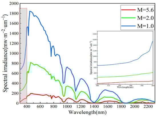
Figure 1.
Spectral irradiance at different relative air qualities.
From Figure 1, it is evident that the spectral radiance intensity exhibits significant variations across different levels of air quality. Specifically, a higher relative air quality corresponds to lower spectral irradiance reaching the ground. The spectral radiance under various relative air qualities was multiplied by the erythema weight and subsequently subjected to integral calculation. To facilitate a comparison, the result at a relative air quality of 5.6 was recorded as 100%. The erythema action spectrum denotes the capacity of UV radiation to induce erythema on human skin, which heavily depends on the wavelength of the radiation [15].
The obtained results are shown in Figure 2.
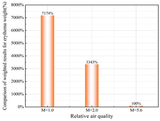
Figure 2.
The results of spectral irradiance weighted by the erythemal action spectrum under different relative air qualities.
The influence of cloud optical thickness on the solar radiation spectrum is shown in Figure 3. Other atmospheric attenuation parameters: relative air quality is 1.5, ozone content is 0.3 cm, water vapor content is 2 cm of deposited water, and surface reflectance is 0.2, and the model is a LOWTRAN Rural (RH is 0~60%) model.
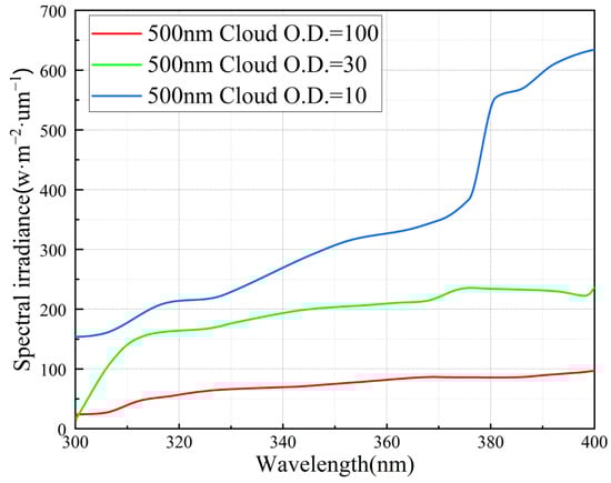
Figure 3.
Variation in spectral irradiance across varying cloud optical thicknesses.
From Figure 3, it can be observed that there is a significant difference in the spectral radiance intensity under different cloud optical thicknesses. As the cloud optical thickness increases, the spectral irradiance reaching the ground decreases. The spectral radiance under various cloud optical thicknesses should be multiplied by the erythema weight, followed by conducting integration calculations. To facilitate a comparison, the results obtained with an optical thickness of 5.6 for the cloud layers are denoted as 100%. The results obtained after spectral weighting by the red band are shown in Figure 4.
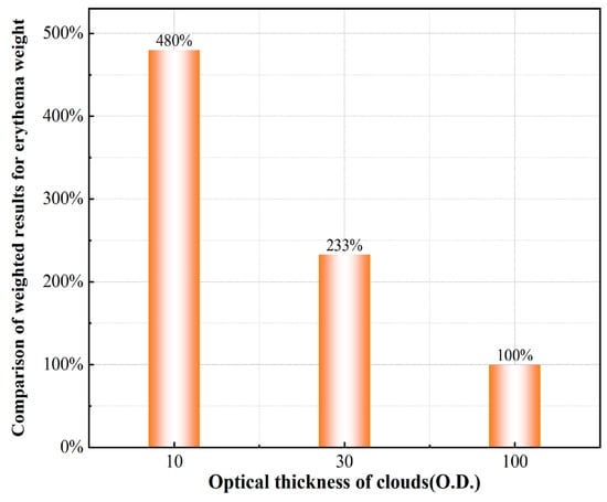
Figure 4.
The results of spectral irradiance weighted by the erythemal action spectrum under different cloud optical thicknesses.
The clouds absorb, scatter, and reflect sunlight, while the processes of light propagation and attenuation within the cloud layer exhibit intricate characteristics. This phenomenon leads to variations in the spectral radiation intensity across different wavelengths, resulting in discrepancies between the light intensity received by detectors and the actual conditions. Additionally, the relative air quality also influences the propagation of solar radiation. In reality, various influencing factors do not occur in isolation but rather interact together, leading to complex variations in the level of ultraviolet radiation over the course of a day and year. Some existing traditional UV detectors assume linear attenuation of solar radiation after it enters the Earth, leading to significant errors in the measured UVI.
2. Novel UV Detector
2.1. Novel Materials and Design Methods for UV Detectors
The present paper introduces a novel ultraviolet detector based on GaN, aiming to address the deficiencies and limitations observed in the aforementioned existing technologies. This detector is characterized by its compact size, high efficiency, absence of the need for an additional filtering apparatus, and capability to accurately monitor the solar UVI. GaN-based materials consist of compounds formed by Group III elements aluminum, gallium, and indium and the Group V element nitrogen (GaN, AlN, and InN), as well as their multicomponent alloys (InGaN, AlGaN, etc.) [16,17,18,19]. In comparison to ultraviolet photodetectors based on silicon materials, ultraviolet detectors utilizing GaN-based materials demonstrate stable physical and chemical properties, as well as robust radiation resistance. The band gap, electron mobility, and saturation drift rates of Si, SiC, and GaN are shown in Table 2 [20,21].
Table 2.
Band gap, electron mobility, and saturation drift rate of Si, SiC, and GaN.
GaN-based material possesses a wide band gap, which allows them to filter out electromagnetic waves with photon energy lower than their band gap. This eliminates the need for costly additional filters required for Si-based detectors. This property presents vast opportunities for the development of emerging electronic and optoelectronic devices, such as ultraviolet detectors. GaN-based materials are considered the most promising semiconductor detectors to replace photomultiplier tubes [22,23,24,25]. In GaN-based materials, the composition of Al and Ga can be varied in order to adjust the threshold energy of photodetectors within the range of 3.4~6.2 eV, thereby covering the ultraviolet wavelength band. This flexibility, which is not found in other semiconductors, makes it highly suitable for the fabrication of ultraviolet photonic devices. Hence, AlxGa1−xN holds immense potential for applications in ultraviolet detection technology [26].
2.2. Structure and Parameters of the New UV Detector
The novel ultraviolet detector proposed in this paper, which utilizes a dual-diode integrated chip, overcomes the challenges associated with material growth and high dark current issues commonly found in high-aluminum components. By fine-tuning the thickness and composition of the short-wave filtering layer, the detector achieves precise alignment with the erythemal response curve. Its structure is depicted in Figure 5.
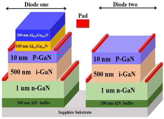
Figure 5.
Schematic diagram of the detector structure.
The detector achieves differentiation by etching to form two distinct structural units. The detector unit one consists of a six-layer epitaxial material structure, resembling a narrow-bandpass PIN ultraviolet detector. The detector unit two consists of a four-layer epitaxial structure, resembling a conventional PIN ultraviolet detector. Both detector units possess the same photosensitive area, with etching that extends into the substrate. Currently, the primary challenge encountered by AlxGa1−xN materials lies in the generation of high-density structural defects within epitaxial AlxGa1−xN films during growth and subsequent growth treatments. The presence of these defects results in high dark currents and unusually large absorption in the visible light range, severely limiting the performance of AlxGa1−xN ultraviolet detectors [27]. The diode one is covered on top with an Al0.4Ga0.6N barrier layer, which has a thickness of 100 nm, and an Al0.33Ga0.67N filter layer with a thickness of 300 nm. The filter layer exhibits a significantly high level of photon absorption intensity for wavelengths below 310 nm. This design obviates the necessity of preparing an AlGaN absorption layer possessing low-density structural defects in order to attain the desired cutoff wavelength.
The light–dark suppression ratio is the ratio of photocurrent to dark current, which essentially represents the UV detector’s ability to suppress noise. Generally, the higher the light–dark suppression ratio, the higher the SNR, and the greater the ability to resist noise. To address the issue of a large lattice mismatch coefficient between AlGaN with a high Al component and the traditional sapphire substrate, as well as the less than ideal thermal mismatch coefficient, a buffer layer is added between the substrate and GaN material. The buffer layer exhibits a relatively low lattice mismatch coefficient with GaN, thereby contributing to the reduction in dislocation density to some extent. Incorporating Al0.33Ga0.67N as the filtering layer in the structure can effectively mitigate high dark current concerns, thereby enhancing the detector’s anti-noise ability. The carrier diffusion in Al0.33Ga0.67N can be effectively suppressed by the 100 nm Al0.4Ga0.6N grown using the MOCVD method, thereby enhancing the short-wave rejection ratio of the diode.
3. Design Results and Analysis
3.1. Simulation Parameter Setting
In order to accurately and truthfully describe the performance of the device, the simulation process will utilize the experimental and published optoelectronic performance as inputs, including absorption coefficient, bandgap, lifetime, generation–recombination model, mobility physical model, and high-field saturation model. The detailed parameters are listed in Table 3.
Table 3.
Parameters [28,29,30,31].
The theoretical calculations have been performed with the SENTAURUS DEVICE, a powerful simulator from Synopsys Incorporated [32]. The Poisson equation and continuity equation were solved for each grid point in the two-dimensional structure while considering three recombination processes: Auger, Shockley-Read-Hall, and photo-generated recombination.
Poisson equation in a steady state:
Continuity equation:
The q represents the charge. Jn and Jp, respectively, denote the electron current density and the hole current density, while p and n represent the hole and electron concentrations. G stands for the carrier generation rate, while R represents the carrier recombination rate.
Hole current and electron current:
3.2. Simulation Results
The response results of Diode Unit one and Diode Unit two are shown in Figure 6.
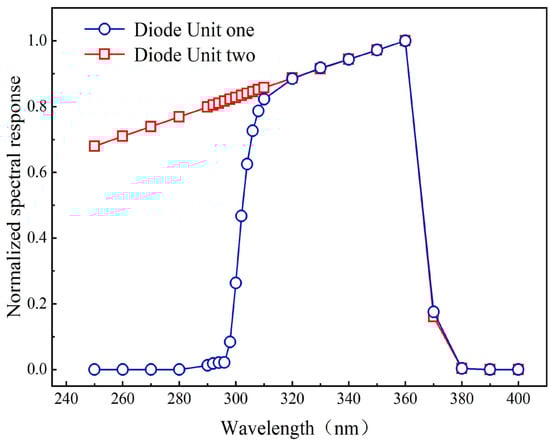
Figure 6.
Normalized spectral responses of Diode Unit one and Diode Unit two.
Due to the utilization of the GaN PIN structure in both Diode Unit one and Diode Unit two, featuring a band gap width of 3.4 eV for GaN corresponding to a wavelength of 365 nm, an evident cutoff at 365 nm is observed in both Diode Unit one and Diode Unit two. Diode Unit one and Diode Unit two are interconnected in a reverse configuration, resulting in an overall response that represents the disparity between their individual responses. The overall normalized spectral response of the device is shown in Figure 7.
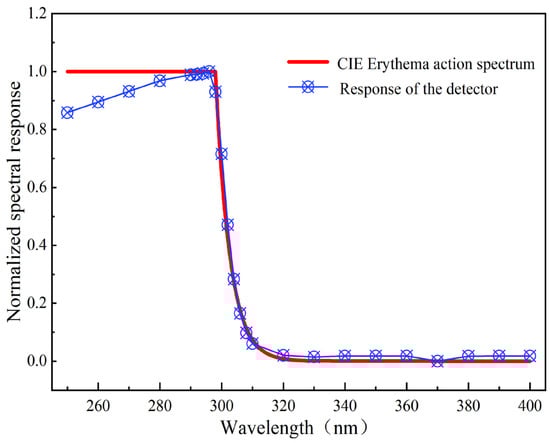
Figure 7.
Normalized spectral response and CIE erythemal action spectrum of the device.
The normalized spectral response of the proposed GaN UV detector closely aligns with the CIE erythemal action spectrum, as depicted in Figure 7.
4. Discussion of the Results
4.1. Comparison of the Spectral Responses
The normalized spectral response of the detector was compared to those of four commercially available UV detectors, as well as the standard erythemal spectral response. These detectors include the Apogee UV detector, XAR-UAB Radiometer, radiometer 5.0, and GaN p-i-n ultraviolet photodetectors [33,34], and the obtained results are shown in Figure 8.
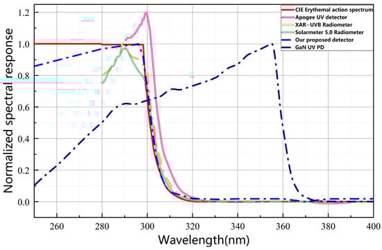
Figure 8.
Normalized spectral response and CIE erythemal action spectrum of multiple detector devices.
The spectral response of the detector is evaluated in relation to the CIE erythemal action spectrum by employing Equation (6), which calculates the mismatch factor for each ultraviolet detector’s ideal spectral response (in comparison to the CIE theoretical response), as expressed in Equation (6) [35].
where Rdevice(λ) represents the normalized spectral response of each detector, and Ser(λ) represents the CIE erythemal action spectrum. The spectrum can be expressed through relatively simple functions within three distinct spectral regions, according to the International Organization for Standardization (ISO).
The mismatch factor of each detector and the response coverage range of each detector are calculated through Equation (8), as shown in Table 4.
Table 4.
Coverage areas and mismatch factors of each detector.
Our proposed detector covers the entire range from 280 nm to 400 nm, with superior matching compared to the detectors currently available on the market. In contrast, the Apogee UV detector only spans from 290 nm to 390 nm, while the XAR-UAB Radiometer covers a range from 210 nm to 380 nm. Additionally, there are discrepancies between the XAR-UAB Radiometer, Apogee UV detector, Solarimeter 5.0 Radiometer, GaN p-i-n ultraviolet photodetectors, and the actual CIE response, with mismatch factors exceeding 10% for each. Thus, in terms of both the coverage range and similarity to the standard CIE response, our proposed detector outperforms the four popular detectors currently on the market.
To obtain the UVI value, it is necessary to multiply the spectral irradiance within a certain wavelength range (250–400 nm) by the erythemal weighting function [36] and then perform an integration calculation.
where Eλ is the solar radiation intensity, Ri(λ) is the spectral response, ker is the constant equal to 40 m2w−1, and each unit wavelength contributes i(λ) = Eλ·Ri(λ) to the output current of the detector. Therefore, we can derive Formula (9):
The spectral response of the detector proposed in this paper exhibits a relatively ideal match with the erythemal action spectrum curve, allowing for the elimination of both Ri(λ) and Ser(λ) within an acceptable margin of error:
The ratio of the detector’s output current to the UV index forms a coefficient, with the detector’s output current directly corresponding to the UV index. Therefore, the calculation expression for the UVI can be represented as
4.2. Experimental Setup
4.2.1. Test Spectra
Below, eight sets of typical ultraviolet radiation spectra [37,38,39] will be selected to compare the measurement accuracy of the detector, utilizing the depicted ultraviolet spectral irradiance in Figure 9.
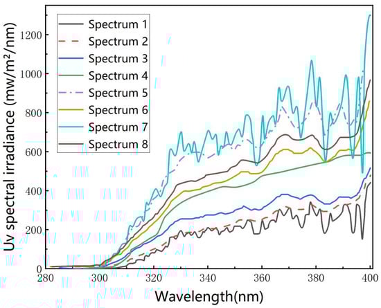
Figure 9.
Ultraviolet spectral irradiance.
4.2.2. UVI Calculation
The overall response of our proposed detector in the wavelength range of 280–400 nm can be expressed by Equation (12):
Replace the standard erythemal response with the spectral responses of various detectors and weigh them with solar radiation under different conditions, as shown in Figure 9.
The results obtained are shown in Figure 10 (sort in ascending order by weight).
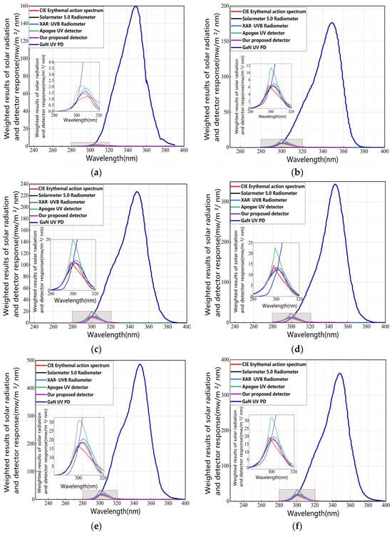
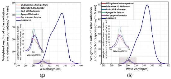
Figure 10.
Spectral 1–8 weighted results. (a) Spectral 1 weighted results. (b) Spectral 2 weighted results. (c) Spectral 3 weighted results. (d) Spectral 4 weighted results. (e) Spectral 6 weighted results. (f) Spectral 8 weighted results. (g) Spectral 5 weighted results. (h) Spectral 7 weighted results.
By comparing the theoretical and actual UVI values obtained from our proposed detector with those from other commercial detectors, it is evident that a significant error arises due to the spectral response of the detector in the UVB band and its mismatch with CIE for UVI measurement. However, there is relatively less error in UVI measurement caused by the mismatch between the detector spectral response and CIE in the UVA and UVC bands. The skin damage caused by solar spectral irradiance primarily occurs in the UVB (280 nm–310 nm) region, which aligns with the weightage assigned to this band according to the CIE action spectrum. This explains why research on ultraviolet radiation measurements has predominantly focused on UVB. Nevertheless, it should be noted that UVA also affects skin health by accelerating darkening and aging processes; however, since it does not have as sensational an association with skin cancer as UVB does, it tends to receive comparatively less attention [40].
4.3. Experimental Results
Using Equation (11) to calculate the theoretical values of the UVI measured by these five detectors and comparing them with the actual UVI, the horizontal axis represents the actual UVI, while the vertical axis represents the theoretical values of UVI measured by these five detectors. The results are shown in Figure 11.
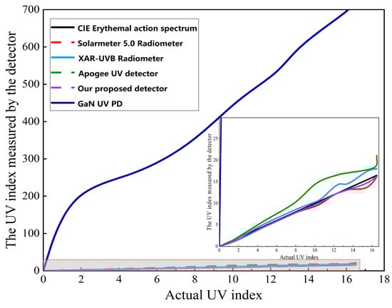
Figure 11.
Comparison of the theoretical and actual values for five detectors.
The results curve indicates that, compared to the mainstream UV detectors currently available on the market, our proposed detector demonstrates a higher similarity between their theoretical weighted results and the standard erythemal weighted results, showcasing their capability for high-precision measurement of the UVI. The measurement error of the UVI of the detector can be calculated using Equation (14):
The UVI obtained through standard erythema weighting is set to the standard value, and the measurement error of each detector is shown in Figure 12.
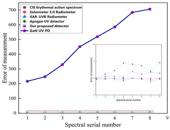
Figure 12.
Theoretical errors of the five detectors.
The experimental results indicate that the miniaturized UV detector proposed in this paper is capable of accurately measuring the UVI in most cases, outperforming the XAR-UVB Radiometer, Apogee UV detector, and Solarmeter 5.0 Radiometer. The short-wave filtering layer of the detector only absorbs short-wave UV radiation, so the signal current does not pass through it. This reduces the requirements for crystal quality and manufacturing costs. The existing commercial silicon photodiodes exhibit a broad spectral response and necessitate the incorporation of an additional optical filter, thereby resulting in escalated manufacturing costs. The Al0.33Ga0.67N layer in the detector structure proposed in this paper has the filtering function itself, so there is no need to add an expensive filter and reduce the manufacturing cost. For AlGaN materials, achieving high-quality (low defect density) AlGaN with increased Al composition is challenging in processing. In this structural configuration, the high-Al content AlGaN material functions solely as a selective filter layer for the efficient absorption of short-wavelength UV light, thereby relaxing the stringent crystal quality requirements for this particular layer. Electrodes are fabricated on GaN material, which can be readily obtained with high-quality crystals through doping and epitaxial growth techniques, resulting in a reduced dark current.
5. Conclusions
In traditional UVI monitoring, the use of erythema response detectors with matching filters presents several issues, including difficulty in controlling the accuracy, large size, high cost, and low measurement precision. The current study presents a GaN-based ultraviolet detector that utilizes an integrated chip mode with a dual-detection unit. The spectral response of the device closely aligns with the erythema spectrum curve established by the World Health Organization, obviating the necessity for supplementary filters. Through the utilization of dual-detector unit matching and the exclusive implementation of epitaxial GaN material as the absorption layer, the challenges associated with growing high-aluminum composition materials and experiencing high dark currents are effectively circumvented. The short-wave filter layer is only used to absorb short-wave ultraviolet light, and the signal current does not pass through this layer, which reduces the requirements for crystal quality and lowers manufacturing costs. The experimental results, demonstrating a measurement error of less than 0.4 when utilizing eight sets of ultraviolet radiation spectra to calculate the performance of the ultraviolet detector, indicate that the portable sunlight UVI monitoring device based on semiconductor ultraviolet photoelectric detectors can accurately and continuously measure the sunlight ultraviolet intensity under diverse conditions in real time. This serves as a reminder for individuals to safeguard themselves and the environment against the detrimental effects of ultraviolet radiation, thereby mitigating potential harm to human health and ecological well-being.
Author Contributions
Conceptualization, H.L. and J.W.; methodology, H.L. and T.L.; software, Y.X.; validation, H.L., D.H. and Y.X.; formal analysis, J.W.; investigation, W.L., J.W., D.H. and Y.X.; resources, T.L. and H.L.; data curation, J.W. and Y.X.; writing—original draft preparation, H.L. and J.W.; writing—review and editing, D.H. and Y.X.; visualization, T.L.; supervision, Y.X.; project administration, H.L. and J.W.; funding acquisition, J.W. All authors have read and agreed to the published version of the manuscript.
Funding
This work was supported in part by the Anhui Provincial Natural Science Foundation (No. 2108085MF228) and Hefei Municipal Natural Science Foundation (No. 2021002).
Institutional Review Board Statement
Not applicable.
Informed Consent Statement
Not applicable.
Data Availability Statement
The data that support the findings of this study are available from the corresponding author upon reasonable request.
Conflicts of Interest
The authors declare no conflicts of interest.
References
- Bojilova, R.; Mukhtarov, P. Dependence of the Index of Biologically Active Ultraviolet Radiation on the Season and Time of Day. Atmosphere 2022, 13, 1455. [Google Scholar] [CrossRef]
- Song, W.; Dai, X. The Gold Nanoparticles Enhanced ZnO/GaN UV Detector. IEEE J. Electron Devices Soc. 2022, 10, 847–853. [Google Scholar] [CrossRef]
- Barnes, P.W.; Robson, T.M. Interactive effects of changes in UV radiation and climate on terrestrial ecosystems, biogeochemical cycles, and feedbacks to the climate system. Photochem. Photobiol. Sci. 2023, 22, 1049–1091. [Google Scholar]
- John, S.M.; Trakatelli, M. Non-melanoma skin cancer by solar UV: The neglected occupational threat. J. Eur. Acad. Dermatol. Venereol. 2016, 30, 3–4. [Google Scholar] [CrossRef] [PubMed]
- Verma, A.; Zanoletti, A. Skin protection from solar ultraviolet radiation using natural compounds: A review. Environ. Chem. Lett. 2024, 22, 273–295. [Google Scholar] [CrossRef]
- Grandahl, K.; Eriksen, P. Measurements of Solar Ultraviolet Radiation Exposure at Work and at Leisure in Danish Workers. Photochem. Photobiol. 2018, 94, 807–814. [Google Scholar] [CrossRef]
- Paulescu, E.; Iman, V.; Dughir, C.; Stefu, N.; Paulescu, M. A Simplified but Accurate UV Index Model. In Proceedings of the 17th Physics Conference (PA), Timisoara, Romania, 25–27 May 2017. [Google Scholar]
- Mazzillo, M.; Shukla, P. 4H-SiC Schottky Photodiode Based Demonstrator Board for UV-Index Monitoring. IEEE Sens. J. 2011, 11, 377–381. [Google Scholar] [CrossRef]
- Zheng, Y.; Sun, C. Integrated Gallium Nitride Nonlinear Photonics. Laser Photonics Rev. 2022, 16, 2100071. [Google Scholar] [CrossRef]
- Makinudin, A.; Haaziq, A. Impact of Crystallinity towards the Performance of Semi-Polar (11–22) GaN UV Photodetector. Mater. Lett. 2021, 286, 129244. [Google Scholar] [CrossRef]
- Wen, F.; Tutuc, E. Strained SixGe1−x-Ge-Si core-double-shell nanowire heterostructures for si-multaneous hole and electron mobility enhancement. Appl. Phys. Lett. 2018, 113, 113102. [Google Scholar] [CrossRef]
- Tang, M. Characteristics, application and development trend of the third-generation semiconductor. Appl. Comput. Eng. 2023, 7, 41–46. [Google Scholar] [CrossRef]
- Xu, J.S.; Li, C.F. Identifying single spin defects in gallium nitride. Nat. Mater. 2024, 23, 447–448. [Google Scholar] [CrossRef] [PubMed]
- Lihua, Z.; Qihuan, T. Solar spectrum distribution in solar radiation test standard. Equip. Environ. Eng. 2017, 14, 65–70. [Google Scholar]
- Webb, A.R.; Slaper, H.; Schmalwieser, A.W. Know Your Standard: Clarifying the CIE Erythema Action Spectrum. Photochem. Photobiol. 2011, 87, 483–486. [Google Scholar] [CrossRef]
- Zhou, S.; Liao, Z. High-Power AlGaN-Based Ultrathin Tunneling Junction Deep Ultraviolet Light-Emitting Diodes. Laser Photonics Rev. 2024, 18, 2300464. [Google Scholar] [CrossRef]
- Fan, B.; Zhao, X. Monolithically Integrating III-Nitride Quantum Structure for Full-Spectrum White LED via Bandgap Engineering Heteroepitaxial Growth. Laser Photonics Rev. 2023, 17, 2200455. [Google Scholar] [CrossRef]
- Zhou, S.; Zhao, X. Application of Patterned Sapphire Substrate for III-Nitride Light-Emitting Diodes. Nanoscale 2022, 14, 4887–4907. [Google Scholar] [CrossRef]
- Zhou, S.; Wan, Z.; Zhao, X. InGaN Quantum Well with Gradually Varying Indium Content for High-Efficiency GaN-Based Green Light-Emitting Diodes. Opt. Lett. 2022, 47, 1291–1294. [Google Scholar] [CrossRef] [PubMed]
- Razeen, A.; Patil, D. Enhanced Performance of Metal-Semiconductor-Metal UV Photodetectors on Algan/Gan Hemt Structure via Periodic Nanohole Patterning. Adv. Mater. Interfaces 2024, 11, 2300726. [Google Scholar] [CrossRef]
- Jiang, H.; Zhang, Y. GaN MSM structure UV photodetector detector based on nonplanar Si substrate and its performance optimization. Semicond. Sci. Technol. 2022, 37, 105020. [Google Scholar] [CrossRef]
- Lv, S.; Wang, S.; Li, L. Gallium Nitride Based Electrode for High-Temperature Supercapacitors. Adv. Sci. 2023, 10, 2300780. [Google Scholar] [CrossRef]
- Su, Y.K.; Peng, S.M. Ultraviolet ZnO Nanorod Photosensors. Langmuir 2010, 26, 603–606. [Google Scholar] [CrossRef] [PubMed]
- Cheng, Z.; Mu, F.W. Interfacial Thermal Conductance across Room-Temperature-Bonded GaN/Diamond Interfaces for GaN-on-Diamond Devices. ACS Appl. Mater. Interfaces 2020, 12, 8376–8384. [Google Scholar] [CrossRef] [PubMed]
- Zhao, H.; Feng, M. Performance improvement of GaN-based microdisk lasers by using a PEALD-SiO2 passivation layer. Opt. Express 2023, 31, 20212–20220. [Google Scholar] [CrossRef] [PubMed]
- Cai, Q.; You, H. Progress on AlGaN-based solar-blind ultraviolet photodetectors and focal plane arrays. Light Sci. Appl. 2021, 10, 244. [Google Scholar] [CrossRef]
- Hu, Y.; Wang, J.; Guo, J.; Chao, G.; Feng, J. Realization of erythemal UV detector using antiparallel connection of the two GaN based photodiodes. In Proceedings of the International Symposium on Advanced Optical Manufacturing and Testing Technologies (AOMATT), Hefei, China, 20 May 2019. [Google Scholar]
- Voevodin, V.I.; Brudnyi, V.N.; Sarkisov, Y.S.; Su, X.; Sarkisov, S.Y. Electrical Relaxation and Transport Properties of ZnGeP2 and 4H-SiC Crystals Measured with Terahertz Spectroscopy. Photonics 2023, 10, 827. [Google Scholar] [CrossRef]
- Liu, Z.; Zhao, D.; Min, T.; Wang, J.; Chen, G.; Wang, H.-X. Photovoltaic Three-Dimensional Diamond UV Photodetector with Low Dark Current and Fast Response Speed Fabricated by Bottom-Up Method. IEEE Electron Device Lett. 2019, 40, 1186–1189. [Google Scholar] [CrossRef]
- Suzuki, N. Nitride Semiconductor Devices: Principles and Simulation, 1st ed.; Piprek, J., Ed.; Wiley: Newark, NJ, USA, 2007; pp. 405–422. [Google Scholar]
- Wang, j.; Guo, J.; Wang, G.; Xie, F.; Jin, L. Improvement of Responsivity of GaN-Based p-i-n Ultraviolet Photodetector by Inserting a Delta Doped Layer in Active Region. In Proceedings of the AOPC 2017: Optical Sensing and Imaging Technology and Applications, Beijing, China, 4–6 June 2017. [Google Scholar]
- Sentaurus Device an Advanced Multidimensional (1D/2D/3D) Device Simulator. Available online: https://www.synopsys.com/manufacturing/tcad/device-simulation/sentaurus-device.html (accessed on 10 July 2024).
- Abdel Baset, Y.; Hamed, S.; Reda, S.; Farag, H.; Ghany, H.; Faramawy, S. Gallium Phosphide (GaP) as a Standard Ultraviolet Index Detector: Response Comparison and Measurements. Phys. Scr. 2023, 99, 10. [Google Scholar] [CrossRef]
- Li, J.; Gao, J.; Ou, B. GaN p-i-n ultraviolet photodetectors grown on homogenous GaN bulk substrates. Solid-State Electron. 2022, 197, 108419. [Google Scholar] [CrossRef]
- ISO/CIE 19476:2014(E); Characterization of the Performance of Illuminance Meters and Luminance Meters. International Organization for Standardization: Geneva, Switzerland, 2014. Available online: https://www.iso.org/obp/ui/en/#iso:std:iso-cie:19476:ed-1:v1:en (accessed on 5 March 2024).
- Kosmopoulos, P.G.; Kazadzis, S. Real-time UV index retrieval in Europe using Earth observation-based techniques: System description and quality assessment. Remote Sens. 2021, 14, 5657–5699. [Google Scholar] [CrossRef]
- Jin, Y.M. Observation and Research on Terrestrial and Atmospheric Solar Radiation in Tibet. Master’s Thesis, Tibet University, Lhasa, China, 2019. [Google Scholar]
- Wang, B. Action spectrum of ultraviolet rays and its measurement. Sol. Energy 2004, 1, 10–11. [Google Scholar]
- Yeo, K.L.; Krivova, N.A. EMPIRE: A Robust Empirical Reconstruction of Solar Irradiance Variability. J. Geophys. Res. 2017, 122, 3888–3914. [Google Scholar] [CrossRef]
- Romanhole, R.C.; Ataide, J.A.; Moriel, P.; Mazzola, P.G. Update on ultraviolet A and B radiation generated by the sun and artificial lamps and their effects on skin. Int. J. Cosmet. Sci. 2015, 37, 366–370. [Google Scholar] [CrossRef] [PubMed]
Disclaimer/Publisher’s Note: The statements, opinions and data contained in all publications are solely those of the individual author(s) and contributor(s) and not of MDPI and/or the editor(s). MDPI and/or the editor(s) disclaim responsibility for any injury to people or property resulting from any ideas, methods, instructions or products referred to in the content. |
© 2024 by the authors. Licensee MDPI, Basel, Switzerland. This article is an open access article distributed under the terms and conditions of the Creative Commons Attribution (CC BY) license (https://creativecommons.org/licenses/by/4.0/).