Abstract
Aimed at the problems of optical frequency combs, such as their large number of comb lines, their high flatness, and their lack of ease in generating, as well as the fact that the channelization efficiency of the scheme based on optical frequency combs is low, we proposed a microwave photonic channelization receiver based on signal polarization multiplexing. Using two-line local optical frequency combs with different frequencies to demodulate the RF signal in the orthogonal polarization state, 16 sub-channels with a bandwidth of 1 GHz can be received simultaneously. The experimental results show that the image rejection ratio can reach 28 dB, and the third-order spurious-free dynamic range of the system can reach 96.8 dB·Hz2∕3. This scheme has the advantages of a large number of sub-channels and a high channelization efficiency; it has great application potential in broadband wireless communication, radar, and electronic warfare systems.
1. Introduction
The rapid development of fields such as radar, electronic warfare, and satellite communication has led to an increasing demand for the bandwidth of signals that can be received. How to achieve the reception of RF signals with an instantaneous bandwidth of several GHz or even tens of GHz is one of the hot topics in current communication technology research [1,2,3]. Digital receivers are currently limited by the sampling rate of analog-to-digital converters and struggle to receive ultra-wideband signals, while analog receivers are constrained by electronic bottlenecks and similarly find it difficult to meet the application requirements for the reception of ultra-wideband signals [4]. Microwave photonics serves as a bridge for conversion between microwave and optical signals; it is capable of converting RF signals that are difficult to directly process into the optical domain for transmission and processing. It offers significant advantages such as large bandwidth, low transmission loss, and strong resistance to electromagnetic interference [5].
Microwave photonic channelized receivers facilitate the complete reception of ultra-wideband RF signals by modulating them into the optical domain and segmenting the spectrum, utilizing multiple spectrally continuous sub-channels for parallel reception. A seminal work in [6] introduced a microwave photonic channelization reception scheme employing coherent dual optical combs, achieving the parallel reception of seven sub-channels, each with a bandwidth of 500 MHz, using two seven-line coherent optical combs with distinct comb–tooth spacings. The authors of [7] presented a channelization reception scheme based on dual optical frequency combs coupled with a Fabry–Perot cavity periodic optical filter. The authors of [8] proposed a channelization scheme leveraging the coherent optical frequency comb and stimulated Brillouin scattering effect. The authors of [9,10] advanced the field with a microwave photonic channelization scheme featuring image suppression down-conversion based on dual coherent optical combs, adept at mitigating post-down-conversion image interference. The authors of [11] introduced an innovative channelization reception scheme based on chirped-pulse linear frequency modulation, utilizing two chirped pulses in place of the dual optical combs. The authors of [12,13] proposed a microwave photonic channelization scheme based on dual micro-ring resonators. The authors of [14] presented a channelization scheme based on polarization-multiplexed optical frequency combs and an integrated coherent receiver (ICR), with additional microwave photonic channelization schemes based on optical frequency combs, as surveyed in [15,16].
Virtually all of the aforementioned approaches necessitate the use of optical comb modules, with the number of sub-channels being limited by the count of teeth in the comb. The creation of optical combs that possess a high number of teeth and a uniform spectral profile continues to pose substantial difficulties, thereby restricting the maximum instantaneous bandwidth that the receiver can handle. This manuscript introduces a microwave photonic channelization reception scheme that leverages signal polarization multiplexing. In comparison to the approach outlined in [14], this scheme is capable of doubling the number of sub-channels to sixteen, under the same premise of utilizing a two-line polarization multiplexed optical comb, which significantly improves the channelization efficiency of the comb.
2. Operation and Principle
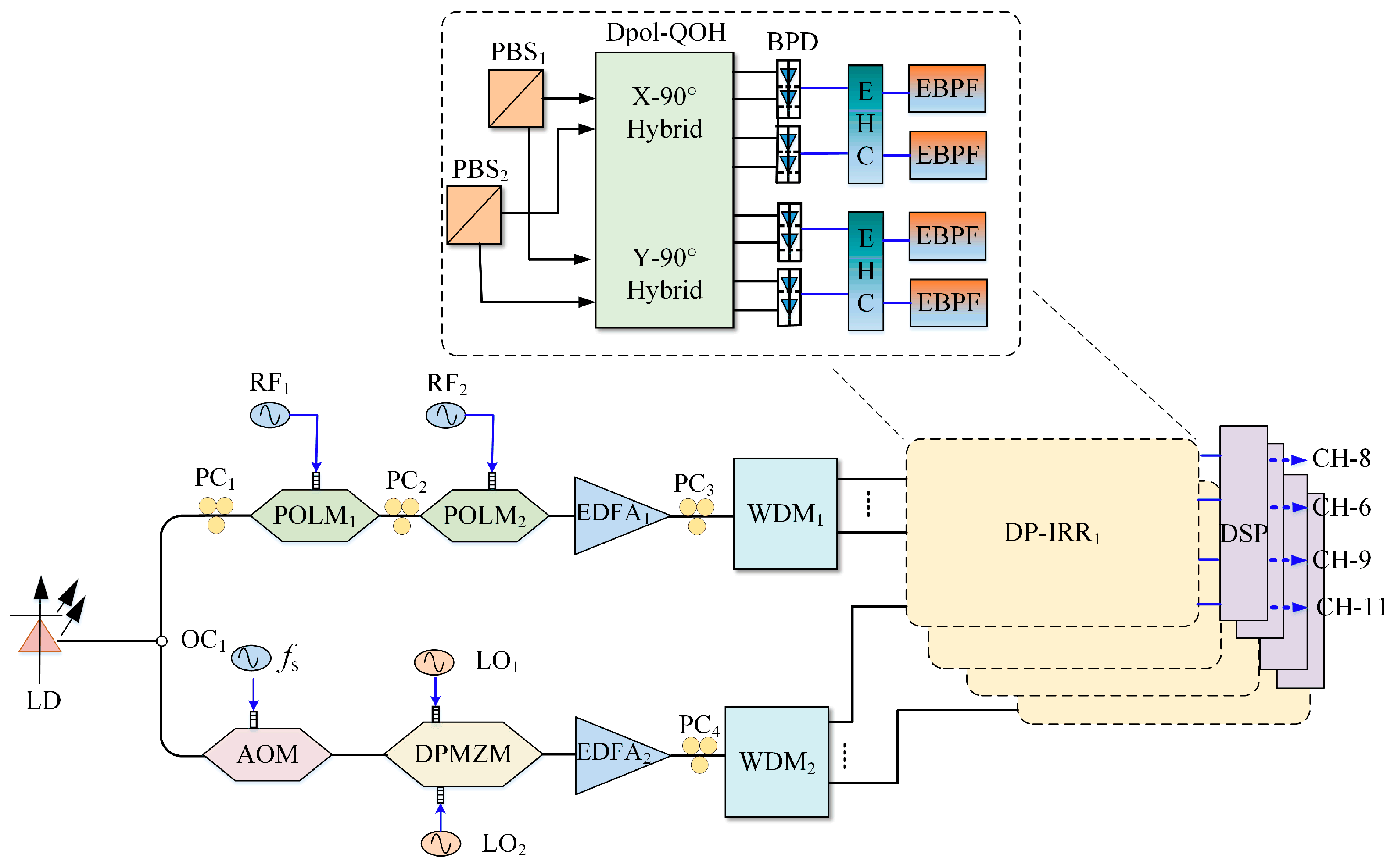
The architecture of the proposed microwave photonic channelized receiver is illustrated in Figure 1. The system is composed of a laser diode (LD), a pair of polarization modulators (POLMs), a pair of erbium-doped fiber amplifiers (EDFAs), an acousto-optic modulator (AOM), a dual-parallel Mach–Zehnder modulator (DPMZM), a quartet of polarization controllers (PCs), a couple of wavelength division multiplexers (WDMs), and a set of four dual-polarization image rejection receivers (DP-IRRs). Each DP-IRR is assembled with two polarization beam splitters (PBSs), a dual-polarization quadrature optical hybrid (Dpol-QOH), a quartet of balanced photodetectors (BPDs), a pair of electrical hybrid couplers (EHCs), and four electrical band pass filters (EBPFs).

Figure 1.
Schematic diagram of the proposed microwave photonic RF channelizer.
The light carrier wave can be expressed as , where E0 and represent the amplitude and angular frequency of the optical signal, respectively. The optical carrier is divided into two paths—upper and lower—by a 50:50 optical coupler. The upper path optical carrier enters POLM1 and is modulated by a single-tone signal. POLM1 has opposite modulation indices in its upper and lower arms, primarily used for generating a polarization multiplexed three-line optical frequency comb. The optical signal output from POLM1 can be represented as follows:
In the context of the provided information, the amplitude of the optical comb is represented by a specific term ; denotes the frequency of the RF1 signal; and is the free spectral range (FSR) of the three-line optical comb. By adjusting the polarization direction of PC2 to form a 45° angle with the principal axes of POLM2, the odd and even order sidebands of the polarization-multiplexed comb are separated by the upper and lower arms of POLM2. The broadband RF signal, RF2, to be received is loaded onto the RF port of POLM2 for signal replication. The output of POLM2 can be expressed as follows:
In the given context, lets denote the modulation index of POLM2 to be , the RF2 signal to be , and the angular frequency of the RF2 signal to be . Assuming the starting and ending frequencies of the RF2 signal are and , respectively, when , the RF sidebands along the orthogonal polarization state completely overlap, as shown in Figure 2a.
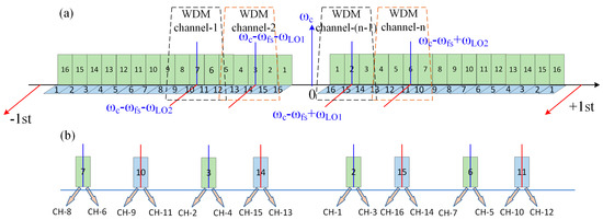
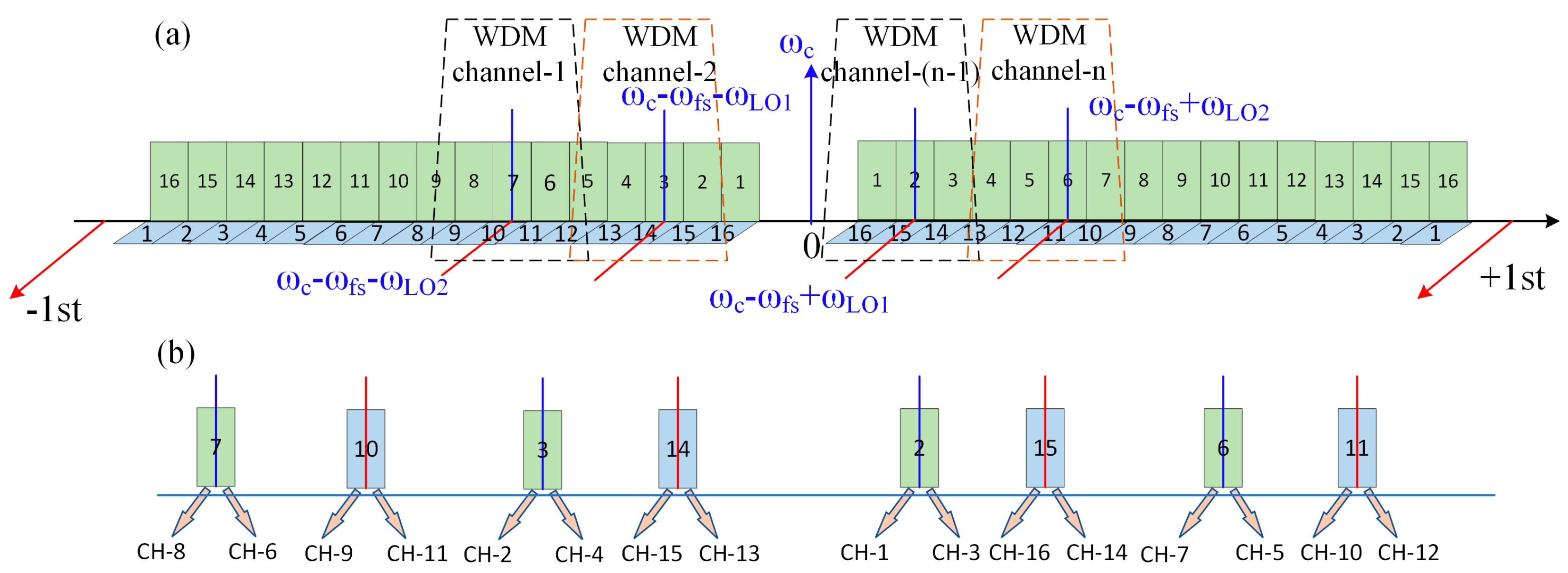
Figure 2.
Spectral diagram of channel reception; (a): before channelization, (b) after channelization.
The lower path optical carrier, after entering the AOM, is modulated by a single-tone signal with a frequency that can be expressed as , where represents the amplitude of the single-tone signal and represents its angular frequency. The AOM then downshifts the optical carrier by a frequency interval of . The output signal from the AOM can be represented as follows:
After the frequency shift, the optical carrier enters a DPMZM and is modulated by two local oscillator (LO) signals, and . Lets denote the amplitudes of LO1 and LO2 to be and , respectively, and their angular frequencies as and , respectively.
Both sub-Mach–Zehnder modulators in the upper and lower arms of the DPMZM operate at the minimum transmission point to perform carrier-suppressed double-sideband (CS-DSB) modulation, while the main modulator operates at the maximum transmission point. Assuming that the higher-order optical sidebands with small amplitudes are negligible, the output optical signal from the DPMZM can be represented as follows:
From Equation (4), it is evident that the DPMZM outputs two sets of dual-line optical combs with different FSRs. Utilizing two wavelength division multiplexers (WDMs) with identical parameters, WDM1 and WDM2, the positive and negative first-order optical sidebands relative to the optical carrier are separated for both the upper and lower paths. The separated RF copy signals and LO signals then enter the same dual-polarization image rejection receiver (DP-IRR) for signal demodulation. The channel reception spectrum is illustrated in Figure 2. It should be noted that at this point, half of the channel requires a simple spectral inversion in the digital domain. Below, we will proceed with the derivation using the WDM’s channel 1 as an example, with the understanding that the demodulation process for other channels is identical to that of channel 1. As can be seen from Figure 2a, channel 1 of the WDM can filter out the LO signal at frequency , as well as several adjacent spectral components that are centered around the RF signal frequencies 7 and 10. For ease of analysis, in the following derivation, the complete RF signal will represent these spectral components of the RF signal.
Adjusting PC3 such that the optical signal output from WDM1 forms a 45° angle with the principal axis of PBS1 results in PBS1 outputting two RF copy signals with different polarization states, namely the X-polarized and Y-polarized signals. The signals output from PBS1 can be represented as follows:
By the same principle, adjusting PC4 ensures that the optical signal output from WDM2 is aligned at a 45° angle to the principal axis of PBS2. At this angle, PBS2 outputs polarization-multiplexed signals that can be represented as follows:
The four optical signals from PBS1 and PBS2 enter a Dpol-QOH, and the output signals can be represented as follows:
The four I/Q signals output after BPD can be represented as follows:
Here, is the photodetector’s responsivity, represents the part of the RF signal spectrum with frequencies higher than the LO signal frequency, and represents the part of the RF signal spectrum with frequencies lower than the LO signal frequency.
At this stage, the four I/Q signals still have spectral aliasing. In the X-polarized state, the LO2 signal with a frequency of , after down-conversion, outputs a mixed signal of the RF signal spectral components 8 and 6, and in the Y-polarized state, it outputs a mixed signal of the RF signal spectral components 9 and 11. The image rejection receiver with a Hartley structure can be utilized to achieve a double output of the image-rejected mixed signals [16]; the principle of image rejection is not elaborated in this paper. Therefore, the four frequency-different LO signals can ultimately demodulate 16 sub-channels, thus achieving the complete reception of the RF signal.
3. Experiment and Results
We have experimentally validated the proposed scheme, achieving complete reception of a broadband signal within the 2–18 GHz range using 16 sub-channels, each with a 1 GHz bandwidth. A continuous optical carrier at a wavelength of 1552 nm, generated by a laser (Emcore 1782), has an output power of 17 dBm. This optical carrier is evenly split into upper and lower paths by a 50:50 optical coupler. The upper path’s optical carrier enters POLM1 (Versawave, PM43AAP) and is modulated by a single-tone signal RF1, producing a polarization-multiplexed three-line optical frequency comb. A broadband signal RF2 with a bandwidth of 40 MHz, generated by an arbitrary waveform generator (Agilent, 8256D), is injected into POLM2 as the signal to be received. The use of a 40 MHz broadband signal for testing is due to experimental constraints that prevent the direct generation of the required broadband RF signal; instead, a series of broadband signals within the 2–18 GHz frequency range with a 40 MHz bandwidth are used to verify the channelization reception function for this frequency segment.
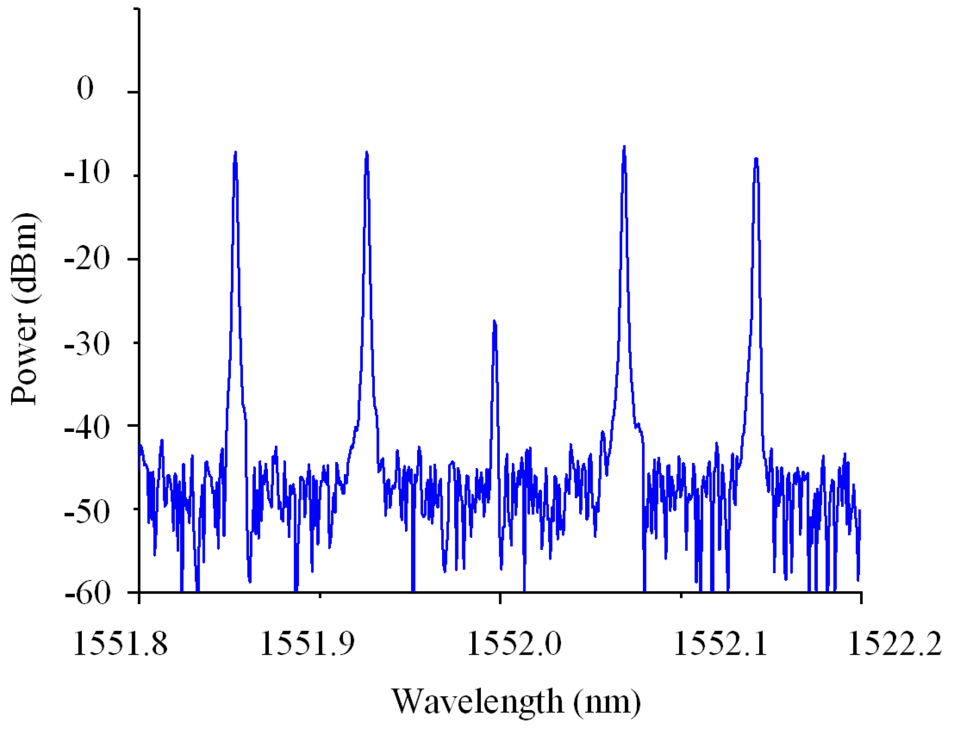
The signal output from POLM2 (Versawave, PM43AAP) is amplified to 18 dBm by an EDFA1 (Keopsys), adjusted in polarization direction by PC1 to an angle of 45° with the PBS1 principal axis, and then channel separation is performed using an OBPF (Yenista XTM-50), followed by connection to the RF input of a DP-IRR. The lower path’s optical carrier is first directed into an AOM (IPF-1000-3FP) to achieve a frequency downshift of 500 MHz. The advantage of using AOM for frequency shifting is that it does not produce spurious harmonics. The frequency-shifted optical carrier then enters the DPMZM (FUJITSU FTM7962EP) on its upper and lower arms, where it is modulated by local oscillator signals LO1 and LO2 with frequencies of 4 GHz and 8 GHz, respectively, for carrier-suppressed double-sideband modulation. The spectrum output from the DPMZM is shown in Figure 3.
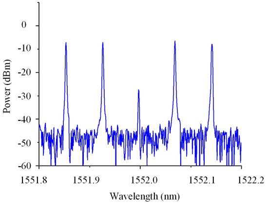
Figure 3.
The output spectrum of the DPMZM.
The signal output from the DPMZM is amplified to 20 dBm by an EDFA2 (Keopsys CEFA-C-HG-PM). After amplification, the signal is adjusted by PC2 to set the angle such that the signal from the DPMZM makes a 45° angle with the principal axis of PBS2. An OBPF (EXFO XTM-50) is then used to direct the optical local oscillator signal with a frequency of into the local oscillator input of the DP-IRR.
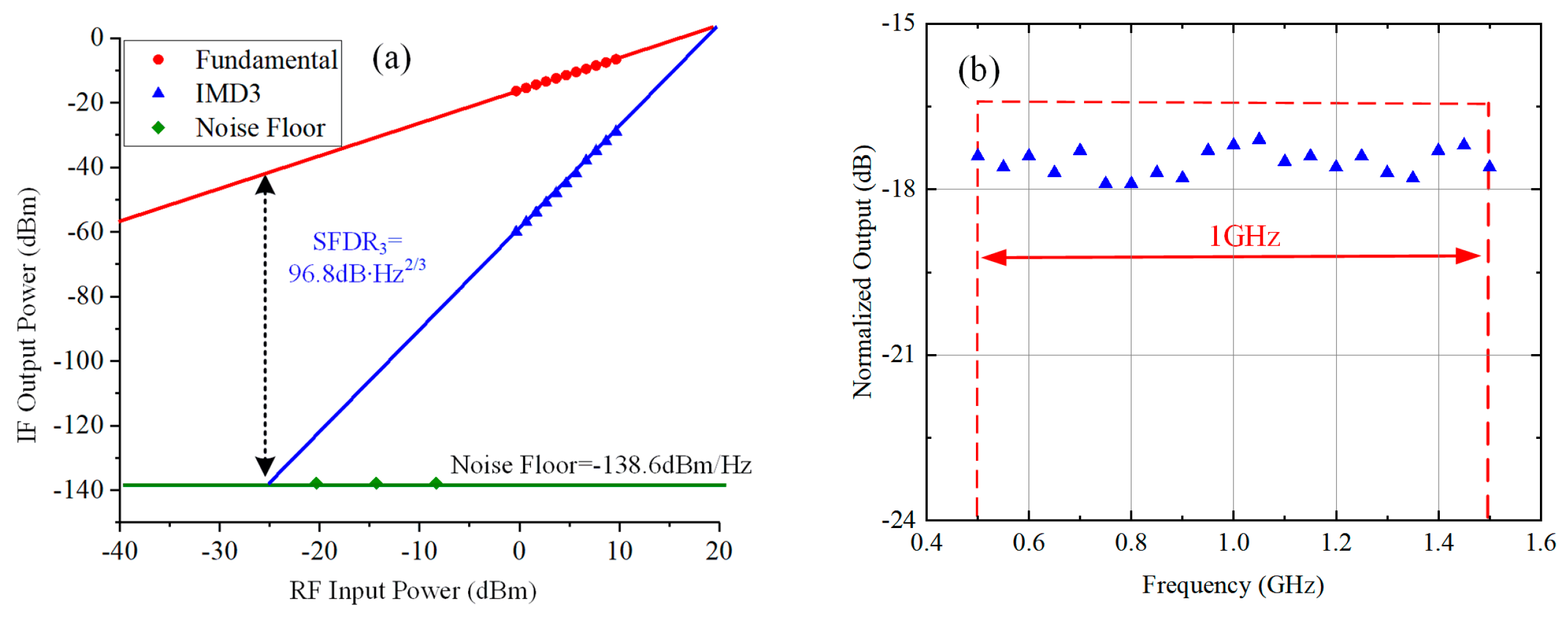
Figure 4a presents the test results for the spurious-free dynamic range (SFDR) of channel 1. The SFDR was measured using a dual-tone signal with central frequencies of 2.8 GHz and 2.81 GHz, down-converted by an LO signal with a central frequency of 3.5 GHz. Table 1 displays the SFDR values for the remaining sub-channels, which are all within the range of 94 dB·Hz2/3 to 96 dB·Hz2/3.
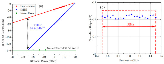
Figure 4.
SFDR measurement results (a) without balanced detection and (b) with balanced detection.

Table 1.
SFDR measurement results for all sub channels.
Figure 4b shows the channel response test results for channel 1. The RF signal was tested for the reception power of all signals within the channel with a starting frequency of 2 GHz, an end frequency of 3 GHz, and a step interval of 50 MHz. The power fluctuation was observed to be within 1.5 dB, indicating that the channel has a good amplitude response. The power fluctuations for the other channels were all found to be less than 2 dB.
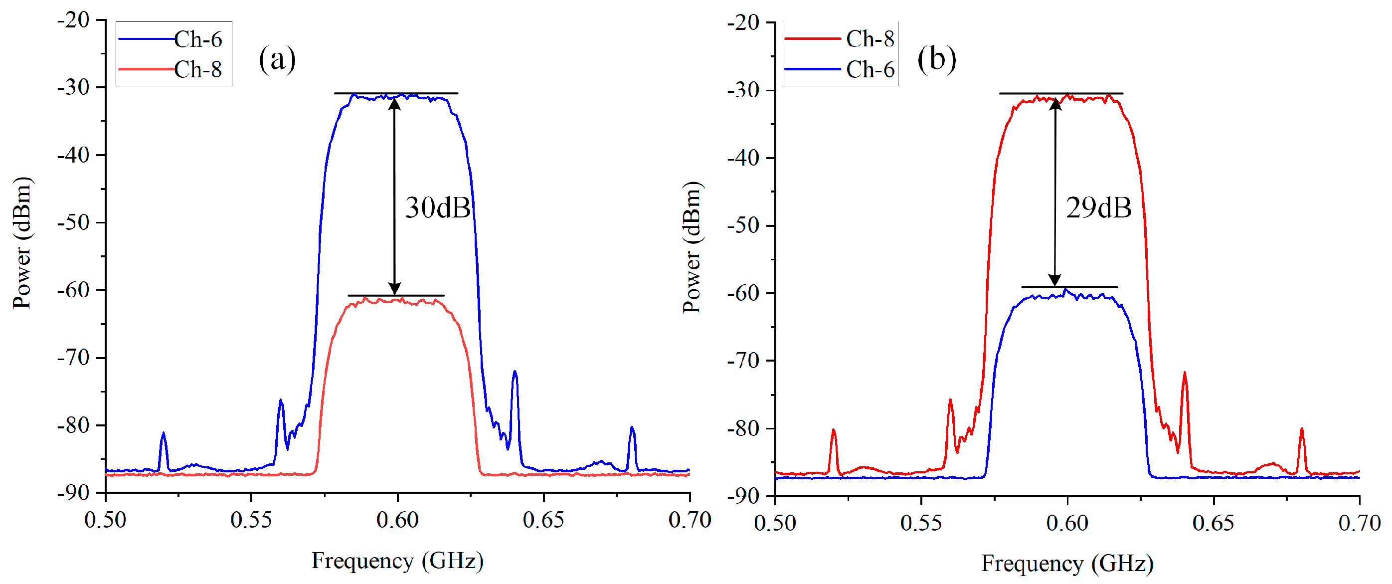
To evaluate the channelization reception and image rejection capabilities within the 2–18 GHz range, we utilized broadband RF signals with a bandwidth of 40 MHz and center frequencies of 7.9 GHz and 9.1 GHz, down-converted with an LO signal at a center frequency of 8.5 GHz. The broadband signal centered at 7.9 GHz, after down-conversion, should be output by channel 6, while the signal centered at 9.1 GHz should be output by channel 8. After image rejection, the DP-IRR1’s X-90° hybrid outputs are expected to deliver channel 6 with 7.9 GHz as the desired signal and 9.1 GHz as the image signal, and channel 8 with 9.1 GHz as the useful signal and 7.9 GHz as the interference signal. The measurement results, as depicted in Figure 5, indicate an image rejection ratio of approximately 29 dB.
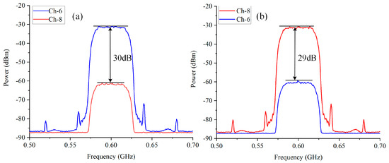
Figure 5.
Electrical spectra of (a) Ch-6 as the desired channel and (b) Ch-8 as the desired channel.
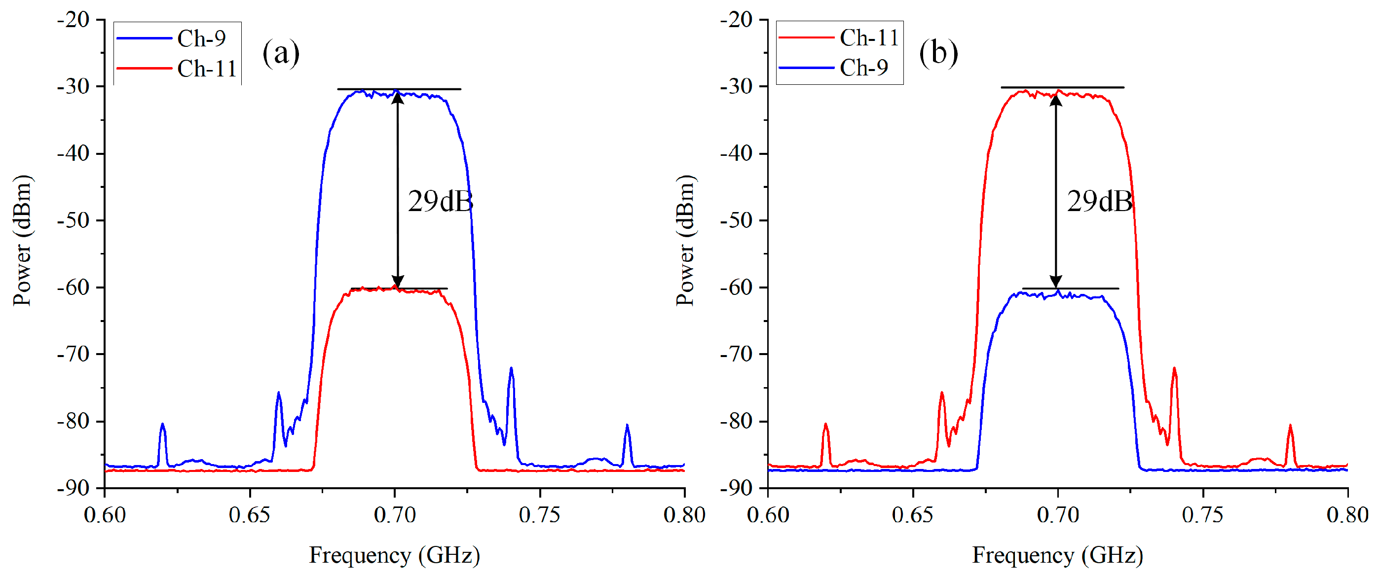
The experiment also conducted the same tests for channels 9 and 11, as well as for channels 1 and 3. The results, shown in Figure 6 and Figure 7, respectively, demonstrate that broadband signals at different frequencies can be accurately output by their corresponding sub-channels, with image rejection ratios consistently around 28 dB.
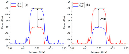
Figure 6.
Electrical spectra of (a) Ch-9 as the desired channel and (b) Ch-11 as the desired channel.
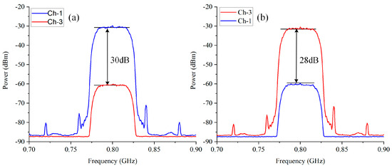
Figure 7.
Electrical spectra of (a) Ch-1 as the desired channel and (b) Ch-3 as the desired channel.
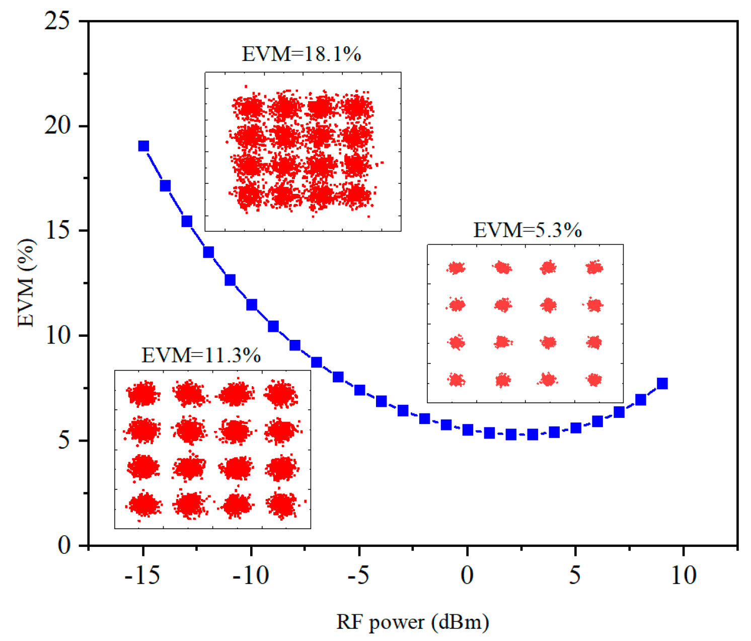
In order to demonstrate that the proposed channelizer can not only receive the broadband RF signal, but also restore the modulated RF signal, an experiment is carried out. A 16-State Quadrature Amplitude Modulation (16QAM) signal with a center frequency of 9.5 GHz is modulated by Quadrature Phase Shift Keying (QPSK) with the symbol rate of 50 MSym/s. After channelization, the IF signal is demodulated by the vector signal analyzer; the constellation diagram is shown in Figure 8. When the power of the input RF signal changes from −15 dBm to −2 dBm, the Error Vector Magnitude (EVM) gradually decreases and reaches the minimum value of 5.3%, which is the best point of communication. When the power of the RF signal changes from −2 dBm to 10 dBm, the EVM begins to increase, which is caused by high-order intermodulation distortion.

Figure 8.
Measured EVM and constellation diagram.
4. Conclusions
This paper investigates a microwave photonic channelization scheme based on signal polarization multiplexing, which modulates the broadband RF signals to be received onto orthogonal polarizations and then demodulates them separately. By utilizing two sets of dual-line optical combs with different FSRs, the scheme can simultaneously receive 16 sub-channels. Its greatest advantage lies in further improving the channelization efficiency of the OFC without increasing the number of comb teeth. The experiment shows that a broadband RF signal covering 2–18 GHz is completely received by 16 sub-channels with a bandwidth of 1 GHz. The in-band interference suppression ratio is 28–30 dB for all sub-channels and the SFDR is about 96 dB·Hz2∕3. In practical applications, in order to achieve automatic polarization adjustment, negative feedback PC can be used, such as commercial polarization trackers (POS-002-E), which can be used in our proposed solution.
Author Contributions
All authors contributed in varying degrees to this paper. B.C.: conceptualization; investigation; methodology; and writing—original draft. J.W.: writing—original draft and editing (equal). Y.L.: methodology (equal). J.T.: methodology (equal). C.L.: supervision. Q.D.: supervision (equal). All authors have read and agreed to the published version of the manuscript.
Funding
This work was supported in part by the Key Research and Development Program of Shaanxi under Grant 2021NY-213 and 2021GY-096, the Special Scientific Research Program of Shaanxi Provincial Department of Education under Grant 23JK0711, and the Xianyang Normal University Research Program under Grants 2023YB62, XSGG202102 and XYSFXY2024023.
Data Availability Statement
The data provided in this study are available upon request from the corresponding author.
Conflicts of Interest
The authors declare no conflicts of interest.
References
- Capmany, J.; Novak, D. Microwave photonics combines two worlds. Nat. Photonics 2007, 1, 319–330. [Google Scholar] [CrossRef]
- Yao, J. Microwave photonics. J. Lightwave Technol. 2009, 27, 314–335. [Google Scholar] [CrossRef]
- Marpaung, D.; Pagani, M.; Morrison, B.; Eggleton, B.J. Nonlinear integrated microwave photonics. J. Light. Technol. 2014, 32, 3421–3427. [Google Scholar] [CrossRef]
- Minasian, R.A. Ultra-wideband and adaptive photonic signal processing of microwave signals. IEEE J. Quantum Electron. 2016, 52, 1–13. [Google Scholar] [CrossRef]
- Wang, Y.; Li, J.; Zhou, T.; Wang, D.; Xu, J.; Zhong, X.; Yang, D.; Rong, L. All-optical microwave photonic downconverter with tunable phase shift. IEEE Photonics J. 2016, 9, 1–8. [Google Scholar] [CrossRef]
- Xie, X.; Dai, Y.; Xu, K.; Niu, J.; Wang, R.; Yan, L.; Lin, J. Broadband photonic RF channelization based on coherent optical frequency combs and demodulators. IEEE Photonics J. 2012, 4, 1196–1202. [Google Scholar] [CrossRef]
- Chong, Y.; Yang, C.; Li, X. A microwave photonic channelization device with common intermediate frequency. J. Optoelect. Laser. 2014, 25, 2294–2299. [Google Scholar] [CrossRef]
- Zou, X.; Li, W.; Pan, W.; Yan, L.; Yao, J. Photonic-assisted microwave channelizer with improved channel characteristics based on spectrumcontrolled stimulated Brillouin scattering. IEEE Trans. Microw. Theory Tech. 2013, 61, 3470–3478. [Google Scholar] [CrossRef]
- Chen, W.; Zhu, D.; Xie, C.; Liu, J.; Pan, S. Microwave channelizer based on a photonic dual-output image-reject mixer. Opt. Lett. 2019, 44, 4052–4055. [Google Scholar] [CrossRef] [PubMed]
- Tang, Z.; Zhu, D.; Pan, S. Coherent Optical RF Channelizer with Large Instantaneous Bandwidth and Large In-Band Inter-ference Suppression. J. Light. Technol. 2018, 36, 4219–4226. [Google Scholar] [CrossRef]
- Hao, W.; Dai, Y.; Yin, F.; Zhou, Y.; Li, J.; Dai, J.; Li, W.; Xu, K. Chirped-pulse-based broadband RF channelization implemented by a mode-locked laser and dispersion. Opt. Lett. 2017, 42, 5234–5237. [Google Scholar] [CrossRef] [PubMed]
- Zhai, W.; Wen, A.; Gao, Y.; Shan, D.; Fan, Y. An Ultraefficient Broadband Photonic Channelizer Based on Polarization-Division Multiplexing and Integrated Dual-Polarization Coherent Detection Receiver. IEEE Trans. Microw. Theory Tech. 2022, 70, 1821–1831. [Google Scholar] [CrossRef]
- Xu, X.; Wu, J.; Nguyen, T.G.; Chu, S.T.; Little, B.E.; Morandotti, R.; Mitchell, A.; Moss, D.J. Broadband RF Channelizer Based on an Integrated Optical Frequency Kerr Comb Source. J. Light. Technol. 2018, 36, 4519–4526. [Google Scholar] [CrossRef]
- Xu, X.; Tan, M.; Wu, J.; Boes, A.; Nguyen, T.G.; Chu, S.T.; Little, B.E.; Morandotti, R.; Mitchell, A.; Moss, D.J. Broadband photonic RF channelizer with 92 channels based on a soliton crystal microcomb. J. Light. Technol. 2020, 38, 5116–5121. [Google Scholar] [CrossRef]
- Xue, X.; Zhang, Y.; Chen, B.; Zhang, Y. Microwave photonic channelizer with large instantaneous bandwidth based on AOFS. IEEE Photonics J. 2021, 13, 5500107. [Google Scholar] [CrossRef]
- Tang, Z.; Pan, S. Image-reject mixer with large suppression of mixing spurs based on a photonic microwave phase shifter. J. Light. Technol. 2016, 34, 4729–4735. [Google Scholar] [CrossRef]

Disclaimer/Publisher’s Note: The statements, opinions and data contained in all publications are solely those of the individual author(s) and contributor(s) and not of MDPI and/or the editor(s). MDPI and/or the editor(s) disclaim responsibility for any injury to people or property resulting from any ideas, methods, instructions or products referred to in the content. |
© 2024 by the authors. Licensee MDPI, Basel, Switzerland. This article is an open access article distributed under the terms and conditions of the Creative Commons Attribution (CC BY) license (https://creativecommons.org/licenses/by/4.0/).