Abstract
Mode converter (MC) is an indispensable element in the mode multiplexing and demultiplexing system. Most previously reported mode converters have been of the transmission type, while reflective mode converters are significantly lacking. In this paper, we propose an ultra-compact reflective mode converter (RMC) structure, which comprises a slanted waveguide surface coated with a metallic film and a subwavelength metamaterial refractive index modulation region. The results demonstrate that this RMC can achieve high-performance mode conversion within an extremely short conversion length. In the two-dimensional (2D) case, the conversion length for TE0–TE1 is only 810 nm, and the conversion efficiency reaches to 94.1% at the center wavelength of 1.55 μm. In a three-dimensional (3D) case, the TE0–TE1 mode converter is only 1.14 μm, with a conversion efficiency of 92.5%. Additionally, for TE0–TE2 mode conversion, the conversion size slightly increases to 1.4 μm, while the efficiency reaches 94.2%. The proposed RMC demonstrates excellent performance and holds great potential for application in various integrated photonic devices.
1. Introduction
In recent years, with the rapid advancement of artificial intelligence and big data, there has been an escalating demand for high-speed information transmission and data processing. Designing and fabricating low-loss and densely integrated photonics chips with substantial information channel capacity have emerged as a noteworthy approach to address this requirement [1,2,3]. Optical waveguides are fundamental components in photonic integrated circuits, utilized for guiding and controlling the propagation of light and for interconnecting different components [4]. Most waveguides rely on a high-refractive-index core layer to confine light through the mechanism of total internal reflection [4]. Additionally, some structures use metallic boundaries to confine light at the interface via surface plasmon polariton (SPP) resonances [5,6]. Another class of waveguides employs periodic photonic crystal structures on either side, where the structural parameters are adjusted to utilize the photonic bandgap effect for confining specific wavelengths of light within the waveguide [7,8]. After careful design, these waveguides have great potential for application in various fields, such as optical information transmission, data processing, sensing, computing, etc. On-chip multiplexing and demultiplexing techniques are promising methods for addressing high-speed information transmission and data processing [9,10], including wavelength division multiplexing (WDM) [11,12], polarization division multiplexing (PDM) [13], and mode division multiplexing (MDM) [14,15]. The MDM system can utilize multiple transmission modes supported by multimode waveguides, and each mode can act as an independent channel to increase optical transmission bottlenecks in data centers, and has attracted intense investigations [16]. For MDM systems, the optical waveguide mode converter is a key device.
Recently, various optical structures and design methods have been developed to achieve mode converters (MCs) for photonic integration. In the initial stages of the development of MCs, the predominant approach involved the utilization of fundamental waveguide configurations. Examples of such structures include directional coupler waveguides [17,18], Mach–Zehnder interferometer structures [19,20], and taper waveguides [21]. The underlying design principle relied on phase matching during coupling or propagation processes. According to the phase-matching principle, the adjustment of structural parameters was undertaken to achieve the desired mode conversion. However, devices designed based on this principle often exhibited large dimensions, typically ranging from tens to hundreds of micrometers [17,18], which adverse to improving the integration level of photonic integrated circuits.
The incorporation of subwavelength dielectric metamaterials and metasurfaces into waveguides facilitates the flexible manipulation of optical fields, enabling the realization of desired light distributions through meticulous design. Consequently, this structure has a wide range of applications in design of compact photonic functional devices, including mode converters [22,23,24,25,26,27]. Researchers have introduced subwavelength metasurface structures into waveguides to design compact mode converters. For instance, in reference [26], they achieved TE0–TE1 mode conversion by designing a high refractive index nanorod metasurface with a periodic gradient of width on the upper surface of the waveguide. The conversion efficiency was 90% at the working wavelength of 1.55 µm, and the conversion length was 20 µm. Researchers have also designed etched dielectric metasurfaces into the waveguide to achieve mode conversion [22,27]. For example, in reference [22], researchers designed shallow-etched periodic metasurfaces in the waveguide for TE0–TE1 mode conversion. The conversion length was 5.75 µm, with an insertion loss of about 1 dB, but a bandwidth of only 20 nm. Additionally, researchers proposed designing a series of etched dielectric hole structures with the same thickness as the waveguide core layer to achieve mode conversion [28,29]. For instance, in reference [28], the researchers achieved TE0–TE1 mode conversion under a small conversion length by adjusting the size of each dielectric hole. The conversion length was 2.42 µm, the maximum conversion efficiency was about 90%, and the bandwidth was 230 nm. However, the minimum characteristic size of the hole structure was only 50 nm, requiring high fabrication precision. Subwavelength grating structures can control the dispersion characteristics and effective refractive index of the waveguide [30,31,32]. Researchers have developed a bricked subwavelength grating waveguide structure to achieve a broadband mode conversion [31]. For TE0–TE1, the conversion length is 9.39 µm, the conversion efficiency is about 91%, the bandwidth with insertion loss less than 1 dB and crosstalk less than −15 dB is 128 nm, and the minimum processing characteristic size is 145 nm. Researchers have successfully achieved the conversion of TE0–TE1 and TE0–TE2 by designing subwavelength dielectric gratings with width gradient changes in waveguides [33]. The conversion efficiency at the center wavelength is approximately 95%. Furthermore, the bandwidth, characterized by an insertion loss of less than 0.65 dB and a crosstalk of less than −10 dB, extends to 407 nm. To the best of our knowledge, this is the state-of-the-art result reported for an ensemble that seems to work well.
In addition, incorporating metallic materials into the waveguide or on the waveguide surface is another method for designing waveguide mode converters [34,35,36]. However, due to the absorption properties of metallic materials, substantial energy loss can occur. For example, in reference [36], a trapezoidal metallic structure was introduced on the waveguide surface to realize TE0–TE1 mode conversion. This converter exhibited a conversion length of 2.5 µm and an insertion loss of up to 1.9 dB. Researchers have also explored phase-changing materials, such as GST and Sb2Se3, for the design of tunable mode converters [37,38]. However, the imaginary part of the refractive index of these materials in the communication band results in some absorption during conversion, making it difficult to achieve low-loss mode conversion over a broad wavelength range. Therefore, despite significant progress, the design of mode converters with ultra-compact dimensions and superior performance remains a challenge that requires further exploration.
One can observe that most of the MCs reported up to now are transmissive configurations. These configurations only utilize a single interaction between the transmitted light field and the structure. In contrast, reflective structures take advantage of dual interactions between the structure and the optical field during the reflection process, offering a promising approach for design innovation. In our paper, we propose a new reflective structure for mode conversion, which consists of a slanted waveguide surface coated with metallic film and subwavelength refractive index modulation. This new reflective structure, after careful design and optimization, can achieve excellent performance in a mode converter with a remarkably short conversion length of 0.8 μm for 2D cases and 1.1 μm for 3D cases. Notably, the conversion length being smaller than the wavelength is a novel finding that has not been previously reported.
2. Design Principle of the RMC
We first analyze a three-layer planar waveguide, as shown in Figure 1. The core material of the waveguide is silicon, and the cladding material is air. The width of the waveguide is w. According to the guiding mechanism of optical waveguides, the width w together with the refractive index determines the types and the number of modes that can be supported within the waveguide. Each mode can be regarded as the superposition of two plane waves with a specific incident angle to the core-cladding interface of the waveguide, i.e., mode angle θ. Therefore, the physical origin of mode conversion is to tune the mode angle from one mode (such as θp for the p-th mode) to that of another (such as θq of the q-th mode).
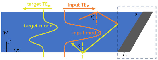
Figure 1.
Schematic diagram of reflective mode conversion (RMC) for a three-layer planar waveguide. The main target for the mode conversion is to make θp and θq different after reflection by the end surface, which satisfies the generalized Snell’s law at the reflection by the end surface.
As shown in Figure 1, incorporate a slanted end face with a slant angle α to tune the incident angle on the side surface of the waveguide. Simultaneously, to ensure total internal reflection at the end face and minimize scattering, a metallic film with a thickness of Lt is deposited on the slant surface.
Now, we design the slanted reflection surface from the viewpoint of metasurface. According to the generalized Snell’s law [26,34] the relationship between the incident angle and the reflection angle to the reflective end surface is given by
where θp and θq represent the mode angle of the incident mode and the corresponding reflection angle of the target mode, respectively. neff is the refractive index of the waveguide, and is the phase gradient induced by the reflective end surface. According to the guiding mode theory, the relationship between the propagation constant of the p-th order mode and the mode angle can be expressed as
According to this relation, the phase gradient required to achieve perfect TEp–TEq mode conversion can be obtained from Equations (1) and (2), which is
where βp and βq are the propagation constants of the TEp and TEq mode, respectively, and k0 is the wave vector in vacuum.
Basically, the phase can be adjusted by changing the slant angle α of the slanted reflective surface. However, adjusting single slant angle α alone does not achieve high efficiency mode conversion (see Figure 2 for details). Since the subwavelength metamaterial can flexibly manipulate the light field, in the subsequent optimization design, we will introduce subwavelength metamaterial units into the waveguide with the slanted reflective surface to achieve the RMC.
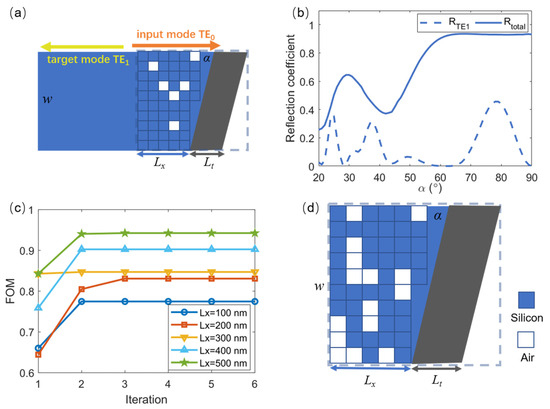
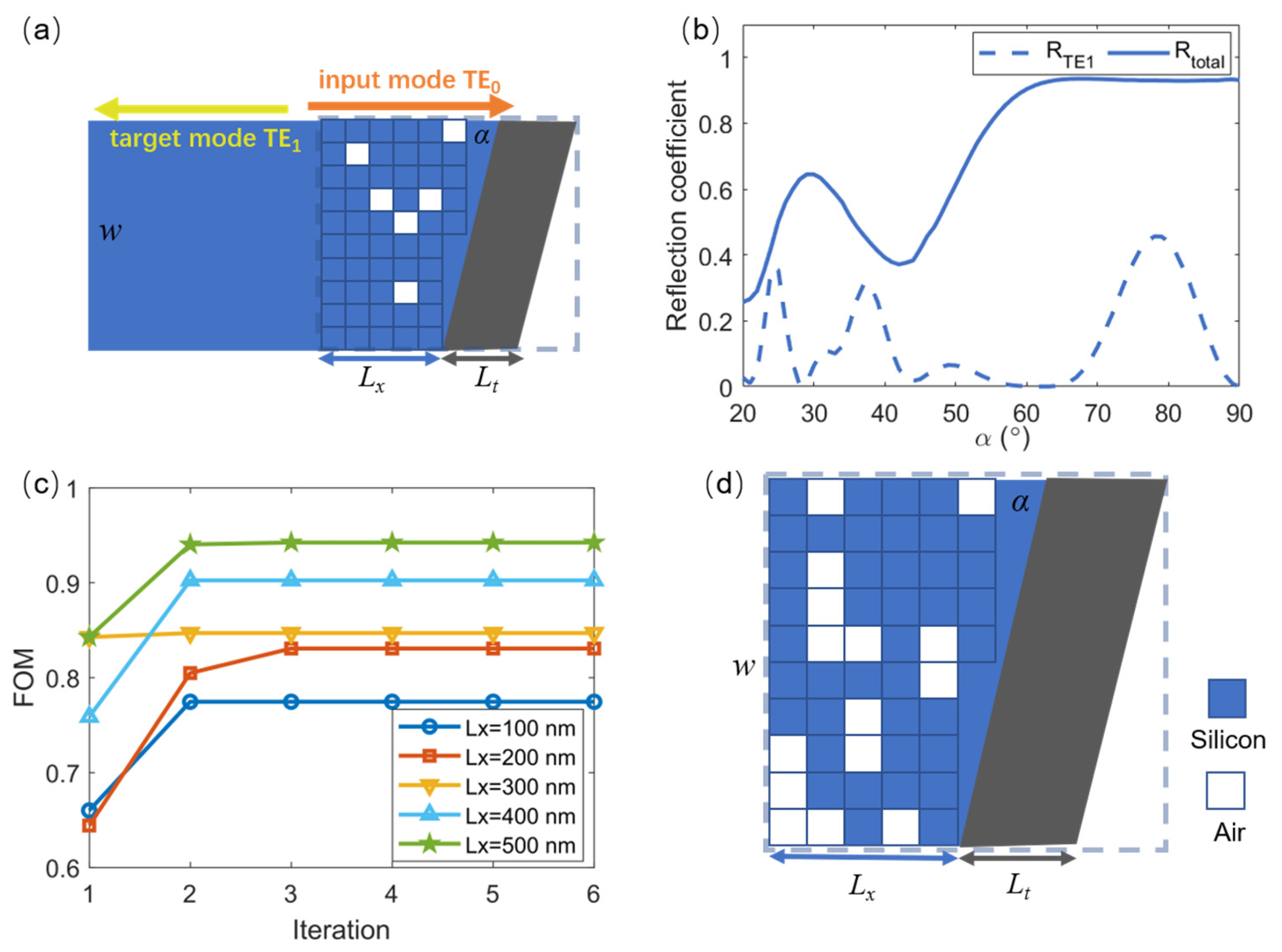
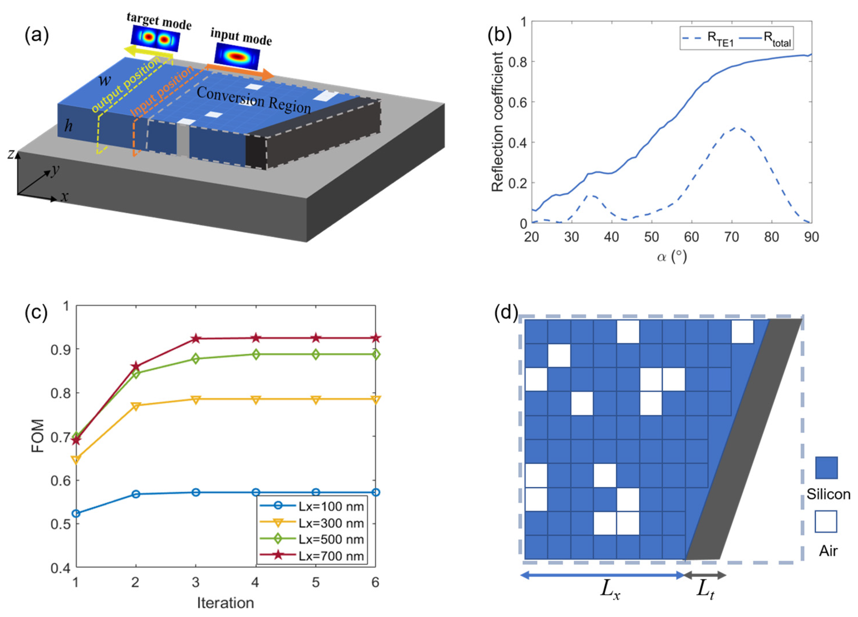
Figure 2.
(a) Schematic diagram of our proposed RMC for 2D planar waveguide. (b) The influence of the waveguide slant angle α on reflectance when TE0 mode is launched in the waveguide. (c) Optimized objective function FOM with different Lx values as a function of iteration numbers. (d) The final optimized conversion region for TE0–TE1 conversion.
3. Optimized Design and Performance Analysis of RMC
3.1. Optimization Design of RMC for 2D Waveguide
To elucidate the model construction and principal analysis process for mode conversion in a more concise and intuitive manner, we initially employ a 2D waveguide as an exemplary case. Specifically, we focus on the design and optimization of the RMC using a 2D planar waveguide, concentrating on the TE0–TE1 conversion. The schematic diagram of the MC is shown in Figure 2a. The light blue dashed box region is the conversion region, which comprises a slanted waveguide with a metallic thin film of thickness Lt (Lt = 100 nm for total reflection) and a subwavelength refractive index modulation region. The material of the metallic thin film is silver. The TE0 mode with a center wavelength of 1.55 µm is launched in the waveguide for forward transmission, and the TE0 mode will be converted to the target TE1 mode for backward reflection by the slanted structure and modulation by the appropriate subwavelength refractive index perturbation. In the design, the width of the waveguide is w = 1000 nm, and the effective refractive index of the TE0 mode is neff0 = 3.410 and that of the TE1 mode is neff1 = 3.205. According to Equation (3), we can obtain the required phase gradient for achieving the TE0–TE1 mode conversion, which is .
As previously mentioned, the first method to adjust the phase gradient is to vary the slant angle α of the slanted waveguide, so we first studied the influence of the waveguide slant angle α on the reflected mode conversion. Mode conversion efficiency is defined as the ratio of the power of the target mode at the output port to the power of the input mode. Using the finite-difference time-domain (FDTD) method, we calculated the energy at the reflected port under different slant angles when the TE0 mode is input to the waveguide, and the reflectivity changing with α is shown in Figure 2b. We noted that the conversion efficiency peaks at an angle of 78°, where the total energy reflectivity is also relatively high. This suggests that, at this angle, the TE0–TE1 mode conversion occurs, and the unnecessary scattering on both sides of the inclination is minimized. This is beneficial for subsequent design considerations. Consequently, we selected this angle as the optimal choice for the subsequent design of the subwavelength refractive index modulation structure.
To achieve high efficiency, we introduced subwavelength metamaterials with spatial refractive index modulation into the slanted waveguide. To obtain suitable spatial refractive index modulation structures for realizing ultra-compact and high-efficiency TE0–TE1 mode conversion, we employed the inverse design method [39,40,41]. The waveguide conversion region is discretized into a series of rectangular pixel unit structures, as shown in Figure 2a. The size of each pixel unit is set to 100 nm, and the material of the pixels is either silicon or air (determined during optimization). The direct binary search (DBS) method [41] is used to optimize the material distribution of the pixel unit in the spatial range of the waveguide at different Lx. The objective function FOM is set to be the conversion efficiency of the TE1 mode. The variation in the objective function with iteration numbers for different Lx is illustrated in Figure 2c, indicating that the highest value of the objective function is achieved at Lx = 500 nm. The conversion region of the optimized RMC is shown in Figure 2d.
The electric field distribution of the RMC after optimization for the TE0–TE1 mode conversion is depicted in Figure 3. When a TE0 mode with a central wavelength of 1.55 µm is input in the waveguide at x = 1.5 µm, it is efficiently converted to the backward-propagating TE1 mode through the combined action of the spatial refractive index modulation and the slanted structure with a metal film, as shown in Figure 3a. The length of the mode conversion area is approximately 810 nm. Figure 3b shows the electric field distribution located at the dashed position in Figure 3a. It can be observed that the converted mode at the reflected output is a relatively well-formed TE1 mode.
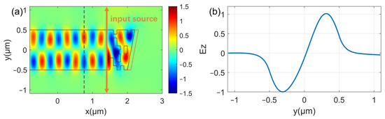
Figure 3.
(a) The electric field distribution of the mode conversion after optimization along the propagation direction. (b) The electric field (Ez) profile at the dashed position in (a).
Next, we analyzed the detailed performance of our optimized 2D RMC. The definitions of the performance parameters are consistent with those provided in the literature [42]. We calculated the changes in device performance parameters at different wavelengths, and the results are shown in Figure 4. The conversion efficiency of the device is greater than 90% in the wavelength range of 1490–1610 nm, the mode purity is greater than 90% in the wavelength range of 1465–1675 nm, the insertion loss is less than 1 dB in the wavelength range of 1455–1695 nm, and the crosstalk is less than −10 dB in the wavelength range of 1445–1660 nm.

Figure 4.
The performance parameters of the 2D RMC. (a) Conversion efficiency. (b) Mode purity. (c) Insertion loss. (d) Crosstalk varies with wavelength for the optimized 2D RMC.
3.2. Optimization Design of RMC for 3D Waveguide
Next, we focus on the optimization design and analysis of the RMC for a 3D waveguide using the same method as presented above, i.e., the slanted reflective end surface and subwavelength refractive index modulation. The 3D RMC is illustrated in Figure 5a. The core material of the waveguide is silicon, while the substrate is silica, and the cladding material is air. The thickness h of the waveguide is set to 220 nm. For the TE0–TE1 mode conversion, the waveguide width w is set to 1000 nm. The area within the dashed box is the conversion region, which includes the slanted waveguide (slant angle α) with a metal film of length Lt (Lt = 100 nm) and a subwavelength refractive index modulation region. The input position is marked with an orange dotted line box, and the output position is marked with a green dotted line box

Figure 5.
(a) Schematic diagram of 3D waveguide RMC structure. (b) The influence of different waveguide slanted angle α on reflectivity when inputting TE0 mode in three-dimensional waveguide. (c) The change in the FOM with the number of iterations under different Lx. (d) The final optimized structure of theTE0–TE1 conversion region.
Similar to 2D structures, we also first adjust the phase change in the optical field by adjusting the slant angle α of the slanted waveguide end surface. Therefore, we calculated the energy transmission at the reflective output port with different slant angles α when the TE0 mode (with a center wavelength of 1550 nm) is launched in the waveguide. The relationship of reflectivity with α is shown in Figure 5b, from which we can obtain that when the slant angle α is 71°. In this case, the maximum reflectivity of the TE1 mode is 47.5%, and the total reflectivity is 77.9%. This result indicates that adjusting the slant angle of the waveguide alone cannot achieve high-efficiency conversion, similar to the case of the 2D structure.
To achieve a high-efficiency 3D RMC with an ultra-compact size, we also introduced subwavelength metamaterial pixels with spatial refractive index modulation into the waveguide based on the aforementioned slanted waveguide structure. The phase and energy transfer distribution of the optical field is modulated by adjusting the subwavelength metamaterial units. Through inverse design, we optimize the spatial refractive index modulation structures to obtain a topological structure that achieves high-efficiency mode conversion. Specifically, the waveguide conversion region is discretized into rectangular pixel units, each with the size of 100 nm × 100 nm and a thickness of 220 nm. Each pixel unit can be made of silicon or air. The DBS algorithm is employed to optimize the material distribution. The optimization objective function FOM is defined as the reflectivity of the target mode (i.e., mode conversion efficiency). We performed optimization calculations for structures with different Lx, and the results showing the variation in the FOM with the number of iterations are presented in Figure 5c. It can be seen that when Lx is 700 nm, the FOM value is the largest, corresponding to a conversion efficiency of 92.5%. Figure 5d shows the final optimized structure of the conversion region.
To more clearly illustrate the performance of our RMC, we calculated the field distribution of the optimized mode converter, as shown in Figure 6. Figure 6a shows the field distribution along the propagation direction at the center (z = h/2) of the waveguide. It can be seen that the input TE0 mode is efficiently converted to the TE1 mode with stable backward transmission after passing through the subwavelength spatial refractive index modulation region and the reflective slanted surface. Notably, the length of the conversion region is only 1.1 µm. Figure 6b shows the optical field at the cross-section of the waveguide output port, which indicates that the output port is a high-purity TE1 mode.
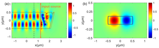
Figure 6.
Field distribution of the optimized mode converter. (a) Field distribution along the propagation direction (xy plane with z = h/2). (b) Cross-sectional field distribution (yz plane) at the output port at the dashed line position in (a).
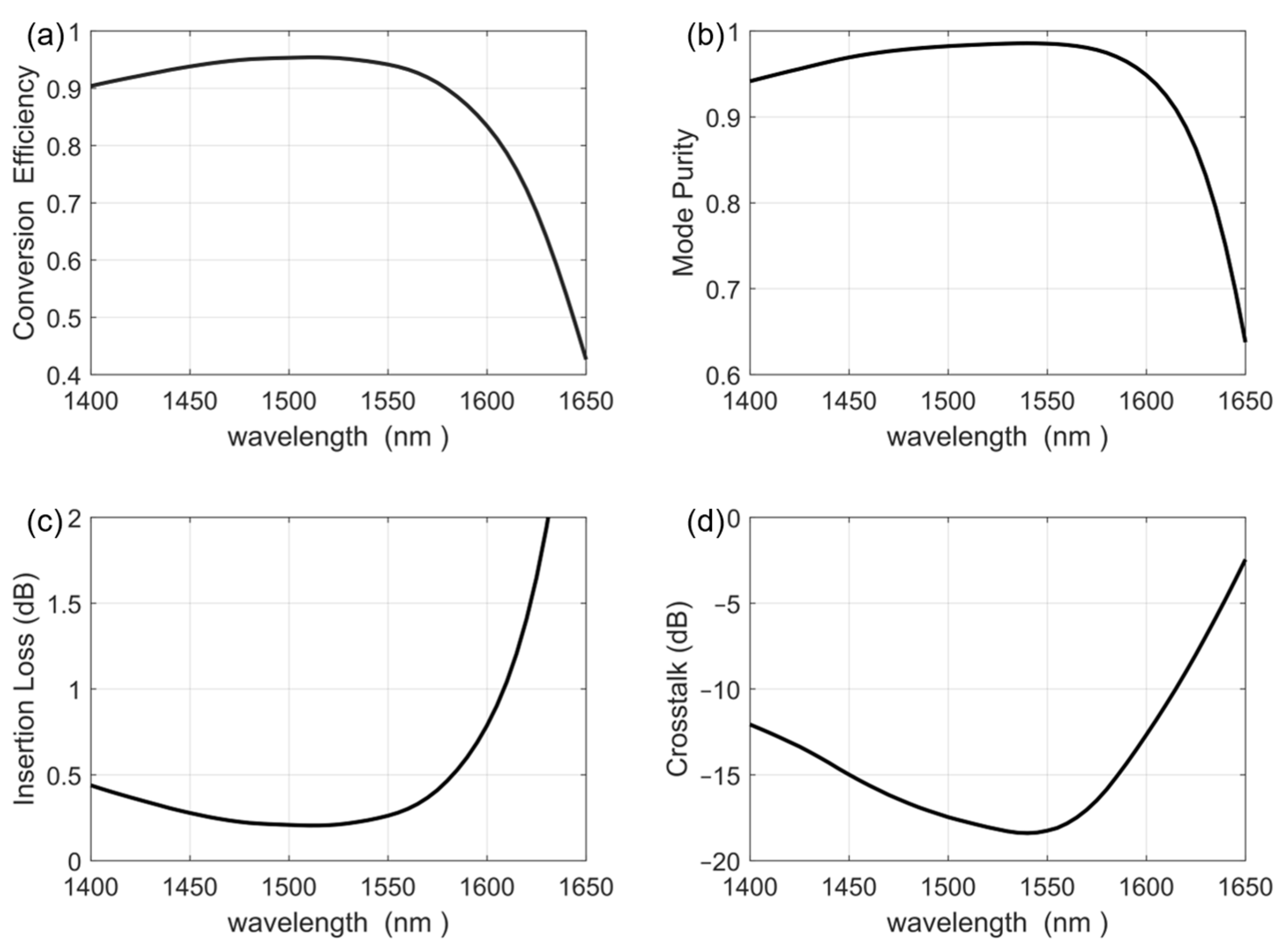
In addition, we calculated the performance of the RMC across different wavelengths, and the results are shown in Figure 7. It can be seen that the conversion efficiency of the device remains greater than 90% in the wavelength range of 1515–1605 nm, and the mode purity is greater than 90% in the wavelength range of 1480–1680 nm. At the same time, the insertion loss is less than 1 dB in 1455–1665 nm, and the crosstalk is less than −10 dB in 1485–1685 nm.
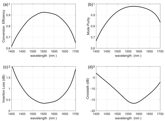
Figure 7.
The performance parameters: (a) conversion efficiency, (b) mode purity, (c) insertion loss, (d) crosstalk under different wavelengths for the optimized three-dimensional waveguide TE0–TE1 mode conversion structure.
In practice, geometric deviations during fabrication are inevitable. Therefore, it is necessary to consider the impact of dimensional errors on the performance of the RMC. Here, we consider two cases: variations in the length and width of the subwavelength rectangular pixel units.
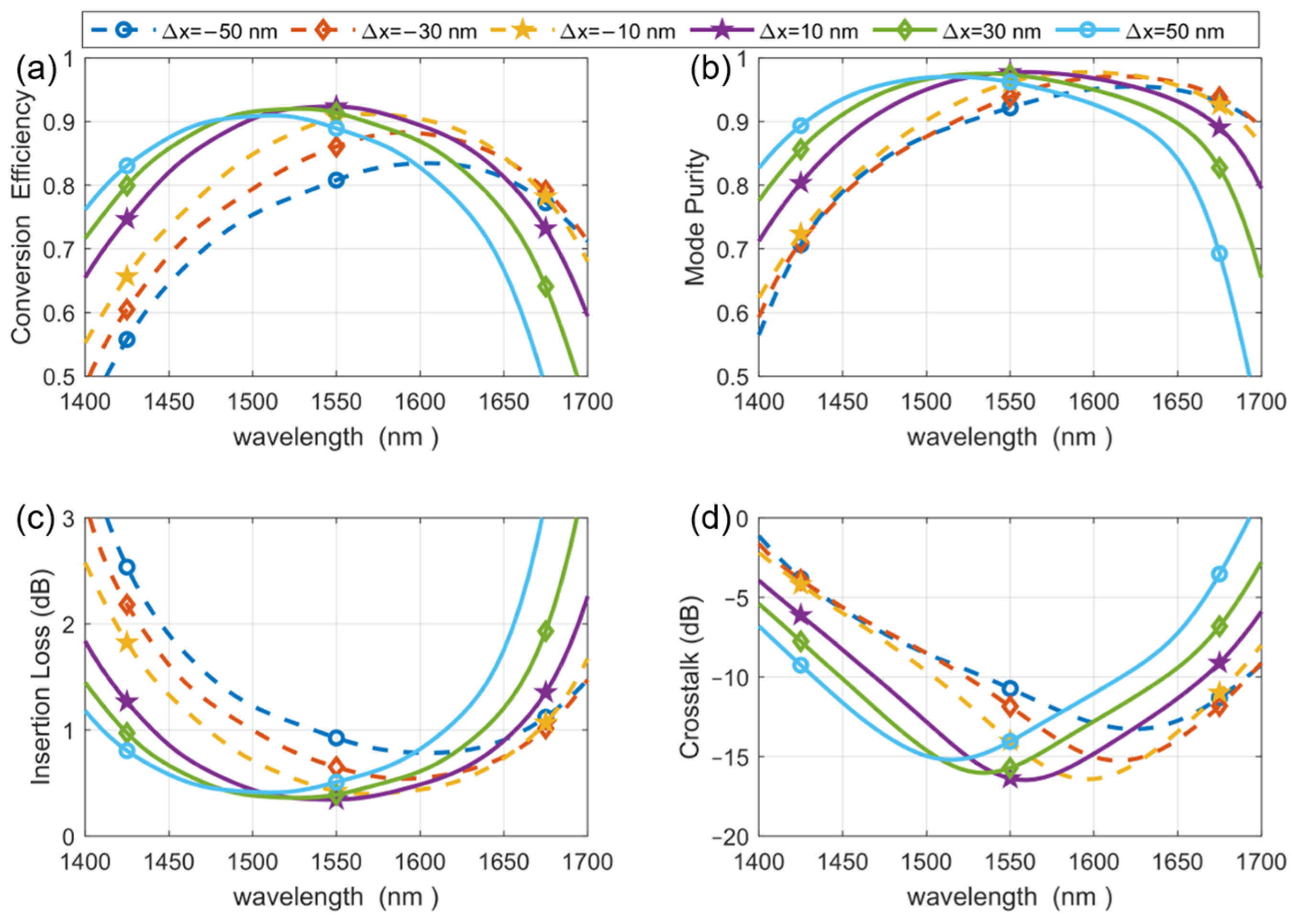
Firstly, we calculated the impact of the length deviation Δx of the pixel units on the mode conversion performance with the deviation Δx between −50 nm and 50 nm, and the results are shown in Figure 8. We found that when Δx is between −10 nm and 50 nm, the conversion efficiency can still be greater than 90% within a wavelength interval of tens of nanometers. When Δx is between −50 nm and 50 nm, the mode purity can be maintained at greater than 90% within a wavelength interval of about 200 nm, and the insertion loss is less than 1 dB within a larger wavelength interval. As Δx decreases, the wavelength interval corresponding to less than 1 dB insertion loss becomes shorter, with the shortest interval of 120 nm. The crosstalk can be maintained at less than −10 dB within a wavelength interval of about 200 nm.
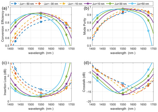
Figure 8.
The impact of the length deviation Δx of the structural units on the mode conversion performance.
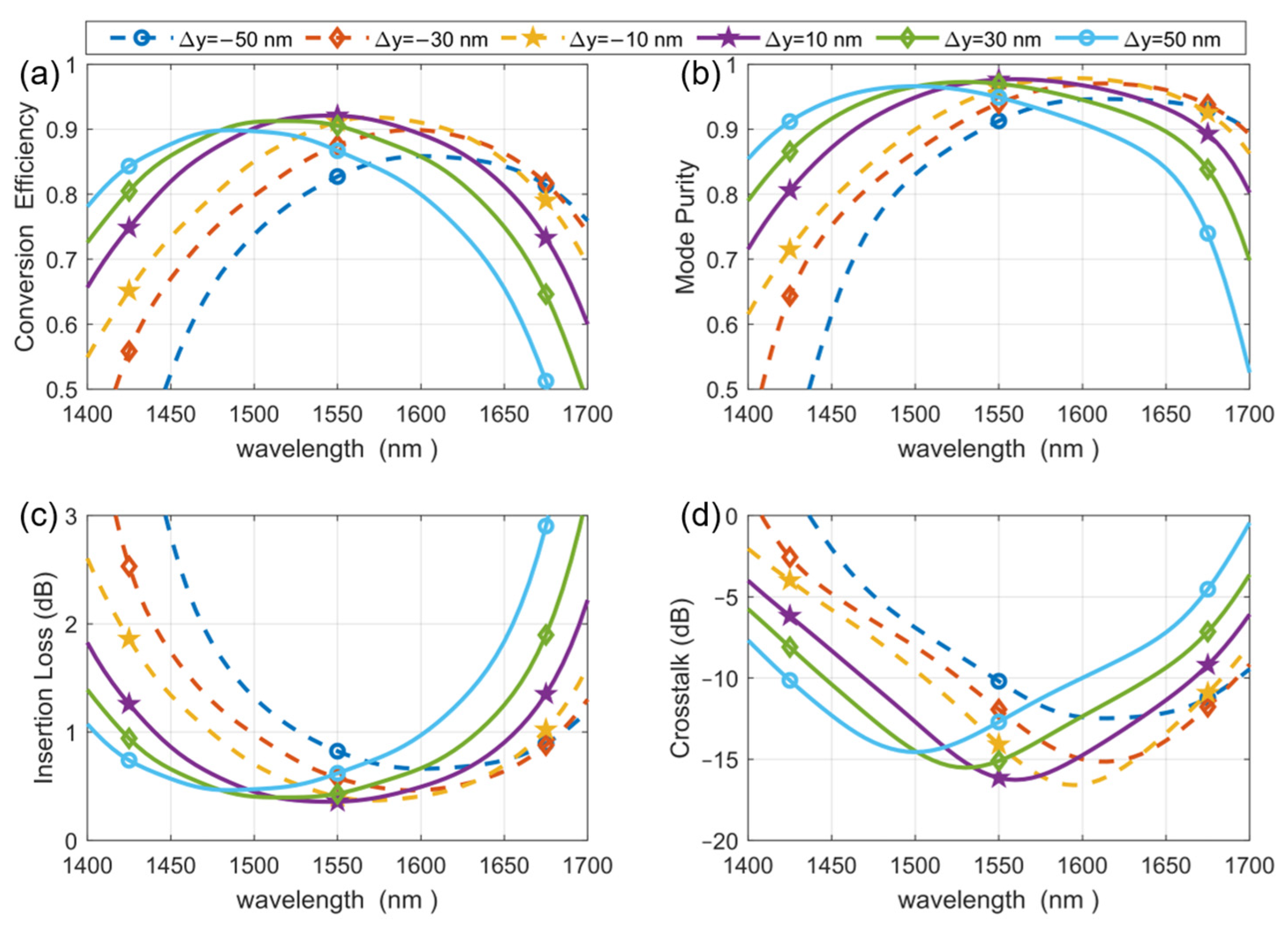
We also calculated the impact of width deviations Δy of the structural units on the mode conversion performance, as shown in Figure 9. When Δy is between −10 nm and 30 nm, the mode conversion efficiency can still be greater than 90% within a wavelength interval of tens of nanometers. When Δy is between −50 nm and 50 nm, the mode purity can be maintained at greater than 90% within a wavelength interval of about 200 nm, and the insertion loss is less than 1 dB within a larger wavelength interval. As Δy decreases, the wavelength interval corresponding to an insertion loss of less than 1 dB becomes shorter, with the narrowest interval of 150 nm occurring at a width deviation Δy of −50 nm. When the processing dimensional deviation Δy is between −50 nm and 50 nm, the crosstalk can be maintained at less than −10 dB within a wavelength interval of about 180 nm. Overall, while the device performance is affected by size deviations of the pixels, it can still maintain good performance with deviations of several tens of nanometers, with maximum mode conversion efficiency remaining above 90% and a 1 dB bandwidth between 150 nm and 200 nm.

Figure 9.
The impact of the width deviation Δy of the structural units on the mode conversion performance.
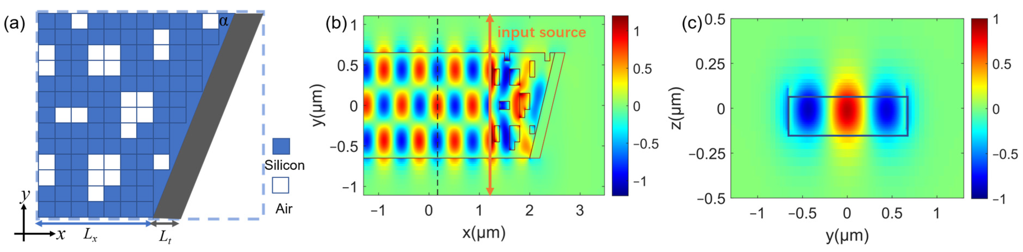
For the conversion of other order modes, optimizing calculations using the same type of structure and method can also achieve an efficient RMC with an ultra-compact size. Here, we designed and analyzed the conversion of TE0–TE2. For the TE0–TE2 conversion, the width w of the waveguide is set to 1300 nm, and the thickness h of the waveguide core layer is 220 nm to ensure that the waveguide supports the transmission of relevant modes. The final conversion region after optimization is shown in Figure 10a, where the end-face slant angle of the waveguide α is 69 degrees, Lx is 700 nm, and Lt is 200 nm. The mode conversion efficiency of the optimized structure at a wavelength of 1.55 µm is 94.1%. The mode field distribution along the propagation direction is shown in Figure 10b. From Figure 10b, it can be seen that the input TE0 mode is well converted to the TE2 mode with stable backward transmission in the reflection direction after passing through the subwavelength spatial refractive index modulation and slanted surface with the metal reflection coating. The length of the conversion region is only 1.4 µm. Figure 10c shows the optical field of the reflected output waveguide cross-section, indicating that the output optical field is a relatively perfect TE2 mode.

Figure 10.
(a) Structure of the optimized conversion region realizing TE0–TE2 conversion. (b) Mode field distribution along the propagation direction. (c) Electric field in the waveguide cross-section at the output port at the dashed position in (b).
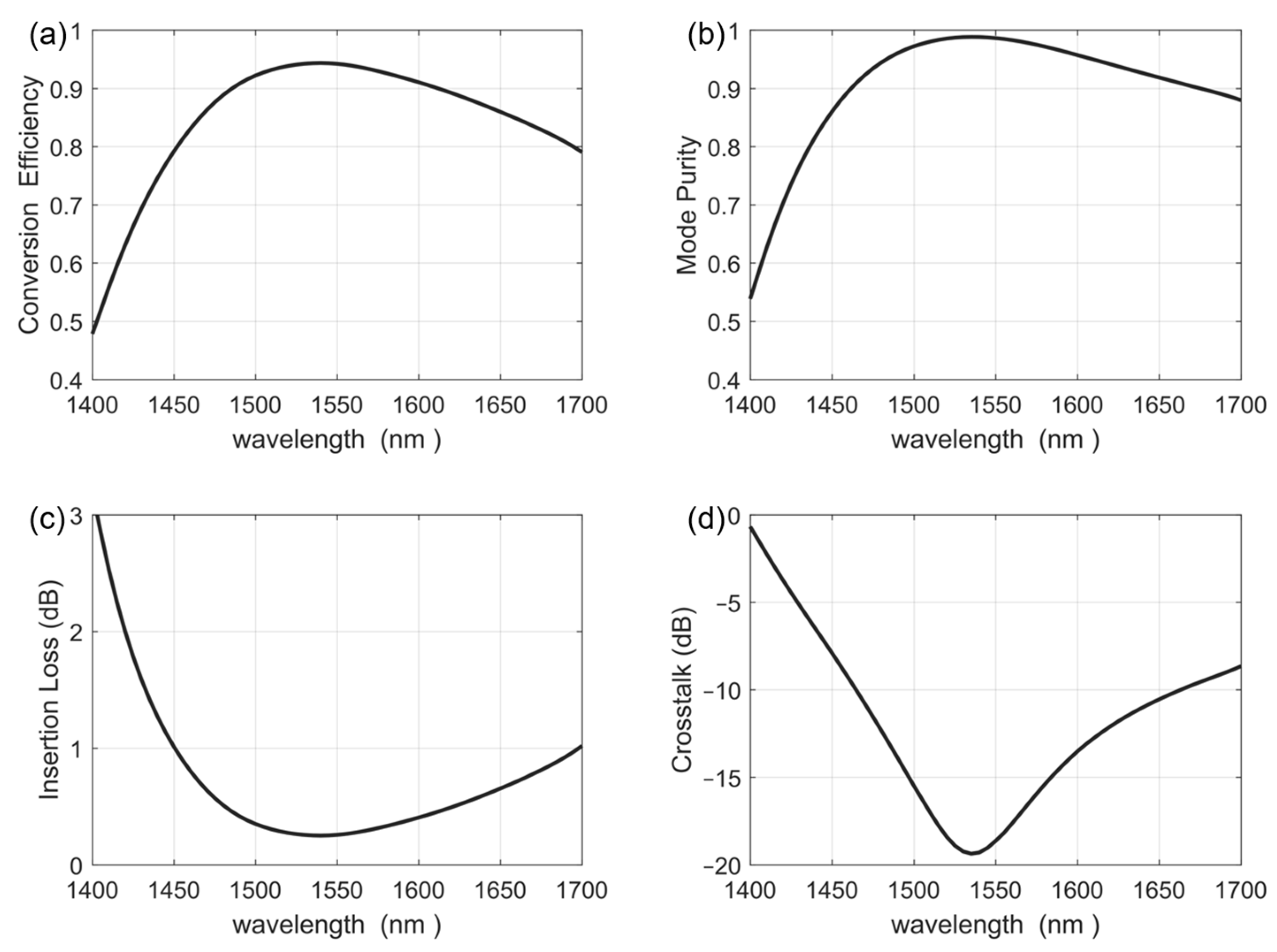
Next, we investigate the bandwidth performance of the optimized TE0–TE2 mode conversion structure, and the results are shown in Figure 11. It can be seen that the conversion efficiency of the optimized TE0–TE2 mode conversion structure is greater than 90% in the wavelength range of 1400–1575 nm, and the mode purity is greater than 90% in the wavelength range of 1400–1615 nm. The insertion loss is less than 1 dB in the wavelength range of 1400–1605 nm, and the total crosstalk of the device is less than −10 dB in the wavelength range of 1400–1610 nm.

Figure 11.
The performance parameters: (a) conversion efficiency, (b) mode purity, (c) insertion loss, (d) crosstalk under different wavelengths for the optimized three-dimensional waveguide TE0–TE2 mode conversion structure.
Table 1 compares our proposed reflective mode converter with other reported mode converters, demonstrating that our design offers great performance at an ultra-compact footprint.

Table 1.
Comparison of the reported mode converters *.
Device fabrication is crucial for realizing the proposed design. The devices we designed can be manufactured using current advanced micro-nanofabrication techniques, as our waveguide’s basic structure is a typical silicon-based strip waveguide with a thickness of 220 nm, which is achievable with existing fabrication methods. Researchers have already successfully fabricated and characterized integrated optical devices based on such waveguide platforms. For fabricating our design, which includes metallic end faces and spatial refractive index modulation structures, appropriate methods are required. This involves cutting the strip waveguide at an angle, depositing a metallic film, and etching rectangular hole structures within the waveguide. Firstly, for angled cutting of the waveguide end face, methods such as femtosecond laser ablation or focused ion beam lithography can be employed. Metal film deposition can be achieved using physical vapor deposition (PVD) or chemical vapor deposition (CVD). To fabricate the spatial refractive index modulation structures, techniques such as electron beam lithography or nanoimprint lithography can be utilized.
4. Discussion
In summary, we proposed a new reflective mode converter based on the combination of the slanted end interface with metallic coating and a short spatial subwavelength metamaterial region. By adjusting the waveguide slant angle and the refractive index distribution region, we achieved the phase and amplitude modulation of the optical mode, thus realizing ultra-compact mode conversion. For the 2D planar waveguide, the conversion length of the designed TE0–TE1 mode converter is only 0.8 µm, with a conversion efficiency of 94.2%. For the 3D TE0–TE1 converter, the conversion length is only 1.14 µm, with a conversion efficiency of 92.5%, an insertion loss of 0.34 dB, and a bandwidth of 180 nm. For the 3D TE0–TE2 converter, the conversion length is 1.4 µm, with a conversion efficiency of 94.1%, an insertion loss of 0.26 dB, and a bandwidth of 205 nm. This new type of mode converter, based on the waveguide end-face slant and subwavelength refractive index modulation, can achieve compact and high-performance operation. The design method may also be applied to other photonic integrated functional devices, such as mode filtering and mode switching.
Author Contributions
Conceptualization, Y.Z. and W.D.; methodology, R.F. and X.L.; formal analysis and numerical simulation, Y.Z., B.S., Q.J. and W.G.; data analysis, Y.Z., Y.G., W.G. and W.D.; writing—original draft preparation, Y.Z. and R.F.; writing—review and editing, Y.Z. and W.D.; project administration, W.D.; funding acquisition, F.S., Y.C. and W.D. All authors have read and agreed to the published version of the manuscript.
Funding
This work was supported by the National Natural Science Foundation of China (Grant No. 12274105); Heilongjiang Natural Science Funds for Distinguished Young Scholar (Grant No. JQ2022A001); The Fundamental Research Funds for the Central Universities (HIT.OCEF.2021020); and the joint guiding project of the Natural Science Foundation of Heilongjiang Province (Grant No. LH2023A006).
Institutional Review Board Statement
Not applicable.
Informed Consent Statement
Not applicable.
Data Availability Statement
Relevant data are available from the authors upon reasonable request.
Acknowledgments
We thank the HPC Studio at the School of Physics, Harbin Institute of Technology, for access to computing resources through INSPUR-HPC@PHY.HIT.
Conflicts of Interest
The authors declare no conflicts of interest.
References
- Khonina, S.N.; Kazanskiy, N.L.; Butt, M.A.; Karpeev, S.V. Optical multiplexing techniques and their marriage for on-chip and optical fiber communication: A review. Opto-Electron. Adv. 2022, 5, 210127. [Google Scholar] [CrossRef]
- Cheng, Q.; Bahadori, M.; Glick, M.; Rumley, S.; Bergman, K. Recent advances in optical technologies for data centers: A review. Optica 2018, 5, 1354–1370. [Google Scholar] [CrossRef]
- Shen, Y.; Meng, X.; Cheng, Q.; Rumley, S.; Abrams, N.; Gazman, A.; Manzhosov, E.; Glick, M.S.; Bergman, K. Silicon Photonics for Extreme Scale Systems. J. Light. Technol. 2019, 37, 245–259. [Google Scholar] [CrossRef]
- Urbonas, D.; Mahrt, R.F.; Stöferle, T. Low-loss optical waveguides made with a high-loss material. Light Sci. Appl. 2021, 10, 15. [Google Scholar] [CrossRef]
- Fang, Y.; Sun, M. Nanoplasmonic waveguides: Towards applications in integrated nanophotonic circuits. Light Sci. Appl. 2015, 4, e294. [Google Scholar] [CrossRef]
- Kazemi, F. Slow light structure implementation to improve Fano response of optical waveguide as a refractive index sensing. Optik 2023, 288, 171189. [Google Scholar] [CrossRef]
- Dutta, H.S.; Goyal, A.K.; Srivastava, V.; Pal, S. Coupling light in photonic crystal waveguides: A review. Photon Nanostruct. Fundam. Appl. 2016, 20, 41–58. [Google Scholar] [CrossRef]
- Maleki, M.J.; Soroosh, M. A novel proposal for performance improvement in two-dimensional photonic crystal-based 2-to-4 decoders. Laser Phys. 2020, 30, 076203. [Google Scholar] [CrossRef]
- Luo, L.-W.; Ophir, N.; Chen, C.P.; Gabrielli, L.H.; Poitras, C.B.; Bergmen, K.; Lipson, M. WDM-compatible mode-division multiplexing on a silicon chip. Nat. Commun. 2014, 5, 3069. [Google Scholar] [CrossRef]
- Yu, Y.; Sun, C.; Zhang, X. Silicon chip-scale space-division multiplexing: From devices to system. Sci. China Inf. Sci. 2018, 61, 080403. [Google Scholar] [CrossRef]
- Liu, D.; Zhang, M.; Shi, Y.; Dai, D. Four-Channel CWDM (de)Multiplexers Using Cascaded Multimode Waveguide Gratings. IEEE Photon Technol. Lett. 2020, 32, 192–195. [Google Scholar] [CrossRef]
- Pan, P.; An, J.; Wang, Y.; Zhang, J.; Wang, L.; Qi, Y.; Han, Q.; Hu, X. Compact 4-channel AWGs for CWDM and LAN WDM in data center monolithic applications. Opt. Laser Technol. 2015, 75, 177–181. [Google Scholar] [CrossRef]
- Wang, J.; He, S.; Dai, D. On-chip silicon 8-channel hybrid (de)multiplexer enabling simultaneous mode- and polarization-division-multiplexing. Laser Photon Rev. 2014, 8, L18–L22. [Google Scholar] [CrossRef]
- Du, J.; Shen, W.; Liu, J.; Chen, Y.; Chen, X.; He, Z. Mode division multiplexing: From photonic integration to optical fiber transmission [Invited]. Chin. Opt. Lett. 2021, 19, 091301. [Google Scholar] [CrossRef]
- Su, Y.; He, Y.; Chen, H.; Li, X.; Li, G. Perspective on mode-division multiplexing. Appl. Phys. Lett. 2021, 118, 200502. [Google Scholar] [CrossRef]
- Xu, H.; Dai, D.; Shi, Y. Silicon Integrated Nanophotonic Devices for On-Chip Multi-Mode Interconnects. Appl. Sci. 2020, 10, 6365. [Google Scholar] [CrossRef]
- Ding, Y.; Xu, J.; Da Ros, F.; Huang, B.; Ou, H.; Peucheret, C. On-chip two-mode division multiplexing using tapered directional coupler-based mode multiplexer and demultiplexer. Opt. Express 2013, 21, 10376–10382. [Google Scholar] [CrossRef] [PubMed]
- Huang, Q.; Wu, Y.; Jin, W.; Chiang, K.S. Mode Multiplexer with Cascaded Vertical Asymmetric Waveguide Directional Couplers. J. Light. Technol. 2018, 36, 2903–2911. [Google Scholar] [CrossRef]
- Sun, C.; Yu, Y.; Chen, G.; Zhang, X. Integrated switchable mode exchange for reconfigurable mode-multiplexing optical networks. Opt. Lett. 2016, 41, 3257–3260. [Google Scholar] [CrossRef]
- Zhao, W.; Liu, R.; Peng, Y.; Yi, X.; Chen, H.; Dai, D. High-performance silicon polarization switch based on a Mach–Zehnder interferometer integrated with polarization-dependent mode converters. Nanophotonics 2022, 11, 2293–2301. [Google Scholar] [CrossRef]
- Chen, D.; Xiao, X.; Wang, L.; Yu, Y.; Liu, W.; Yang, Q. Low-loss and fabrication tolerant silicon mode-order converters based on novel compact tapers. Opt. Express 2015, 23, 11152–11159. [Google Scholar] [CrossRef] [PubMed]
- Wang, H.; Zhang, Y.; He, Y.; Zhu, Q.; Sun, L.; Su, Y. Compact Silicon Waveguide Mode Converter Employing Dielectric Metasurface Structure. Adv. Opt. Mater. 2018, 7, 1801191. [Google Scholar] [CrossRef]
- Xiang, J.; Tao, Z.; Li, X.; Zhao, Y.; He, Y.; Guo, X.; Su, Y. Metamaterial-enabled arbitrary on-chip spatial mode manipulation. Light Sci. Appl. 2022, 11, 168. [Google Scholar] [CrossRef] [PubMed]
- Ohana, D.; Levy, U. Mode conversion based on dielectric metamaterial in silicon. Opt. Express 2014, 22, 27617–27631. [Google Scholar] [CrossRef] [PubMed]
- Liang, Y.; Xu, Y.; Dong, Y.; Zhang, B.; Ni, Y. Efficient silicon-based higher-order mode converters based on subwavelength grating slots. J. Opt. Soc. Am. B 2021, 38, 2908–2914. [Google Scholar] [CrossRef]
- Li, Z.; Kim, M.-H.; Wang, C.; Han, Z.; Shrestha, S.; Overvig, A.C.; Lu, M.; Stein, A.; Agarwal, A.M.; Lončar, M.; et al. Controlling propagation and coupling of waveguide modes using phase-gradient metasurfaces. Nat. Nanotechnol. 2017, 12, 675–683. [Google Scholar] [CrossRef] [PubMed]
- Zhou, H.; Wang, Y.; Gao, X.; Gao, D.; Dong, J.; Huang, D.; Li, F.; Wai, P.A.; Zhang, X. Dielectric Metasurfaces Enabled Ultradensely Integrated Multidimensional Optical System. Laser Photon Rev. 2022, 16, 2100521. [Google Scholar] [CrossRef]
- Yao, C.; Wang, Y.; Zhang, J.; Zhang, X.; Zhao, C.; Wang, B.; Singh, S.C.; Guo, C. Dielectric Nanoaperture Metasurfaces in Silicon Waveguides for Efficient and Broadband Mode Conversion with an Ultrasmall Footprint. Adv. Opt. Mater. 2020, 8, 2000529. [Google Scholar] [CrossRef]
- Dou, T.; Yue, S.; Wang, R.; Hou, Y.; Shi, H.; Zhang, Z.; Liu, Y.; Xue, M.; Zhang, Z. Ultra-compact and ultra-broadband arbitrary-order silicon photonic multi-mode converter designed by an intelligent algorithm. Opt. Express 2023, 31, 9481–9495. [Google Scholar] [CrossRef]
- Sun, L.; Zhang, Y.; He, Y.; Wang, H.; Su, Y. Subwavelength structured silicon waveguides and photonic devices. Nanophotonics 2020, 9, 1321–1340. [Google Scholar] [CrossRef]
- Lu, M.; Deng, C.; Sun, Y.; Wang, D.; Huang, L.; Liu, P.; Lin, D.; Cheng, W.; Hu, G.; Lin, T.; et al. Compact and broadband silicon mode-order converter using bricked subwavelength gratings. Opt. Express 2022, 30, 24655–24666. [Google Scholar] [CrossRef] [PubMed]
- Luque-González, J.M.; Ortega-Moñux, A.; Halir, R.; Schmid, J.H.; Cheben, P.; Molina-Fernández, Í.; Wangüemert-Pérez, J.G. Bricked Subwavelength Gratings: A Tailorable On-Chip Metamaterial Topology. Laser Photon Rev. 2021, 15, 2000478. [Google Scholar] [CrossRef]
- Guo, J.; Ye, C.; Liu, C.; Zhang, M.; Li, C.; Li, J.; Shi, Y.; Dai, D. Ultra-Compact and Ultra-Broadband Guided-Mode Exchangers on Silicon. Laser Photon Rev. 2020, 14, 2000058. [Google Scholar] [CrossRef]
- Yu, N.; Genevet, P.; Kats, M.A.; Aieta, F.; Tetienne, J.-P.; Capasso, F.; Gaburro, Z. Light Propagation with Phase Discontinuities: Generalized Laws of Reflection and Refraction. Science 2011, 334, 333–337. [Google Scholar] [CrossRef] [PubMed]
- Abu-Elmaaty, B.E.; Shalaby, H.M.H. Highly efficient silicon mode converter and polarization rotator using a silicon-based hybrid plasmonic waveguide. J. Opt. Soc. Am. B 2023, 40, 2789–2795. [Google Scholar] [CrossRef]
- Xu, Y.; Liu, L.; Hu, X.; Dong, Y.; Zhang, B.; Ni, Y. Scalable silicon-based mode-order converters assisted by tapered metal strip layer. Opt. Laser Technol. 2022, 151, 108028. [Google Scholar] [CrossRef]
- Chen, H.; Jia, H.; Yang, J.; Tian, Y.; Wang, T. Ultra-compact switchable mode converter based on silicon and optical phase change material hybrid metastructure. Opt. Commun. 2020, 473, 125889. [Google Scholar] [CrossRef]
- Fei, Y.; Xu, Y.; Dong, Y.; Zhang, B.; Ni, Y. Nonvolatile phase change material based multifunctional silicon waveguide mode converters. Opt. Laser Technol. 2024, 168, 110006. [Google Scholar] [CrossRef]
- Mao, S.; Cheng, L.; Zhao, C.; Khan, F.N.; Li, Q.; Fu, H.Y. Inverse Design for Silicon Photonics: From Iterative Optimization Algorithms to Deep Neural Networks. Appl. Sci. 2021, 11, 3822. [Google Scholar] [CrossRef]
- Jia, H.; Zhou, T.; Fu, X.; Ding, J.; Yang, L. Inverse-Design and Demonstration of Ultracompact Silicon Meta-Structure Mode Exchange Device. ACS Photon 2018, 5, 1833–1838. [Google Scholar] [CrossRef]
- Shen, B.; Wang, P.; Polson, R.; Menon, R. An integrated-nanophotonics polarization beamsplitter with 2.4 × 2.4 μm2 footprint. Nat. Photon 2015, 9, 378–382. [Google Scholar] [CrossRef]
- Zhang, Y.; Feng, R.; Shi, B.; Jia, Q.; Li, H.; Li, X.; Sun, F.; Cao, Y.; Ding, W. Ultra-compact mode converter based on longitudinal refractive index modulation. Opt. Commun. 2024, 554, 130197. [Google Scholar] [CrossRef]
- Guo, Z.; Xiao, J.; Wu, S.; Lai, Y.; Cheng, S. Compact, Scalable and Flexible Multi-Mode-Converting Model Employing Subwavelength Gratings. J. Light. Technol. 2024, 1–14. [Google Scholar] [CrossRef]


Disclaimer/Publisher’s Note: The statements, opinions and data contained in all publications are solely those of the individual author(s) and contributor(s) and not of MDPI and/or the editor(s). MDPI and/or the editor(s) disclaim responsibility for any injury to people or property resulting from any ideas, methods, instructions or products referred to in the content. |
© 2024 by the authors. Licensee MDPI, Basel, Switzerland. This article is an open access article distributed under the terms and conditions of the Creative Commons Attribution (CC BY) license (https://creativecommons.org/licenses/by/4.0/).