Article

Terahertz CMOS High-Sensitivity Sensor Based on Hybridized Spoof Surface Plasmon Resonator

1
State Key Laboratory of Millimeter Waves, Southeast University, Nanjing 210096, China
2
Institute of Electromagnetic Space, Southeast University, Nanjing 210096, China
3
Jiangsu Provincial Hospital of Traditional Chinese Medicine, Nanjing 210029, China
4
National Mobile Communications Research Laboratory, Southeast University, Nanjing 210096, China
*
Authors to whom correspondence should be addressed.
Photonics 2025, 12(2), 102; https://doi.org/10.3390/photonics12020102
Submission received: 5 December 2024 / Revised: 17 January 2025 / Accepted: 21 January 2025 / Published: 23 January 2025
(This article belongs to the Special Issue New Trends in Terahertz Photonics)

Abstract

:
In recent years, spoof localized surface plasmon (SLSP) have gained increasing attention due to their strong electromagnetic wave confinements. Based on the multipole resonance of SLSP, a high-Q-factor terahertz resonator based on CMOS technology is proposed. Specifically, a quadrilateral hybridized SLSP structure, composed of a core and a cavity SLSP resonator, is designed to reduce electric dimension and improve the Q-factor. The experimentally measured Q-factor reached 56.7 at 194 GHz, which is quite a high value within the terahertz frequency band, particularly given the compact electrical dimension of 0.081λ × 0.081λ. Moreover, pharmaceutical testing in the terahertz frequency range was successfully conducted, including glucose and two traditional Chinese medicines: Chuanbei and Sanqi. And three frequency shifts (4 GHz, 3.2 GHz, and 1.4 GHz) were observed. Thus, the SLSP resonator holds great potential for high-performance terahertz applications.

1. Introduction

Studies on sensors have been conducted throughout the wave spectra for a long time. In the optical regime, research on optical sensor is flourishing [1]. With the advantages of compact size and high sensitivity, optical sensors have been employed in a series of scenarios, such as humidity sensing [2], refractive index sensing [3], temperature sensing [4], etc. Interactions between light and matter can be enhanced utilizing optical resonance like microcavity [5] and surface plasmon (SP) [6]. Moreover, the quality factor (Q-factor) of the optical sensor could reach as high as 108, guaranteeing great sensing precision and enabling single-molecular sensing [7]. In the terahertz band, the low photon energy allows for nondestructive detection, and can penetrate dielectric materials, making it suitable for high-sensitivity detection and sensing applications [8], which have attracted increasing interest [9,10,11]. However, due to the small dimension of the terahertz device, precision of PCB technology is insufficient to meet the requirement. Consequently, semiconductor technologies such as CMOS have been adopted for terahertz design in recent years, which provide the advantage of high precision in the terahertz band [12,13,14]. The design of surface plasmon resonator based on CMOS is attractive, as this type of work has not been widely explored.
SP have attracted intense attention for their ability to confine and enhance fields at the metal–dielectric interface in the optical and far-infrared frequency bands [15,16]. According to the propagation characteristics, surface plasmon can be categorized into two types, surface plasmon polariton (SPP) and localized surface plasmon (LSPs), which are localized near the metal particles. By introducing the corrugated structure, SPP and LSP [17] can be mimicked in the lower-frequency band, such as the microwave band [18,19,20]. The corrugated structures in the terahertz and microwave band were named spoof surface plasmon polariton (SSPP) [21] and spoof localized surface plasmon (SLSP) [22,23]. In 2014, a planar SLSP resonator with nearly zero thickness was proposed with a sensing experiment conducted in the microwave band, holding promising potential in integrated plasmonic circuits and systems [24].
Research in this area has been driven by a series of pioneering works. Kim et al. [25] designed a SLSP resonator for sensing glucose concentration. With an elaborately designed microfluidic channel, glucose concentration variation could be detected according to the changes in the S parameter at 28 GHz. Zhou et al. [26] excited higher-radial-order SLSP for terahertz on-chip sensing. Although the SLSP exhibit a high Q-factor, the dimension of the SLSP resonator needs further reduction. The hybridization of plasmons introduces a highly sensitive resonance characteristic to SLSP, which makes them good candidates for sensors and detectors [7,27]. A hybridized SLSP resonator was designed with a concentric structure [28]. The spokes on the inner and outer SLSP resonators could generate a large coupling, which offers the advantages of compact size, high Q-factor, and high environmental sensitivity.
In this work, we propose a novel hybridized square quadrilateral resonator structure based on SLSP fabricated using CMOS technology. This hybridized resonator structure consists of two coupled SLSP resonators, a core resonator and a cavity resonator. Gratings are incorporated in both the outer and inner LSPs resonators, which are tightly interconnected to reduce the electrical size, with a total area of 126 × 126 μ m 2 . Experimental measurements show a Q-factor of 56.7 at 194 GHz. In addition, we performed pharmaceutical testing experiments on three medicinal solutions: glucose, Chuanbei, and Sanqi. The results conclusively demonstrate that the hybridized SLSP resonator offers exceptional sensitivity for medicinal detection in the terahertz frequency range, indicating a substantial potential as a chip-based sensor.
This article is organized as follows: Section 2 introduces the designs and simulation results of the proposed SLSP resonator; Section 3 performs the sensing simulation; Section 4 presents the experimental results of the SLSP; and Section 5 draws the conclusion.

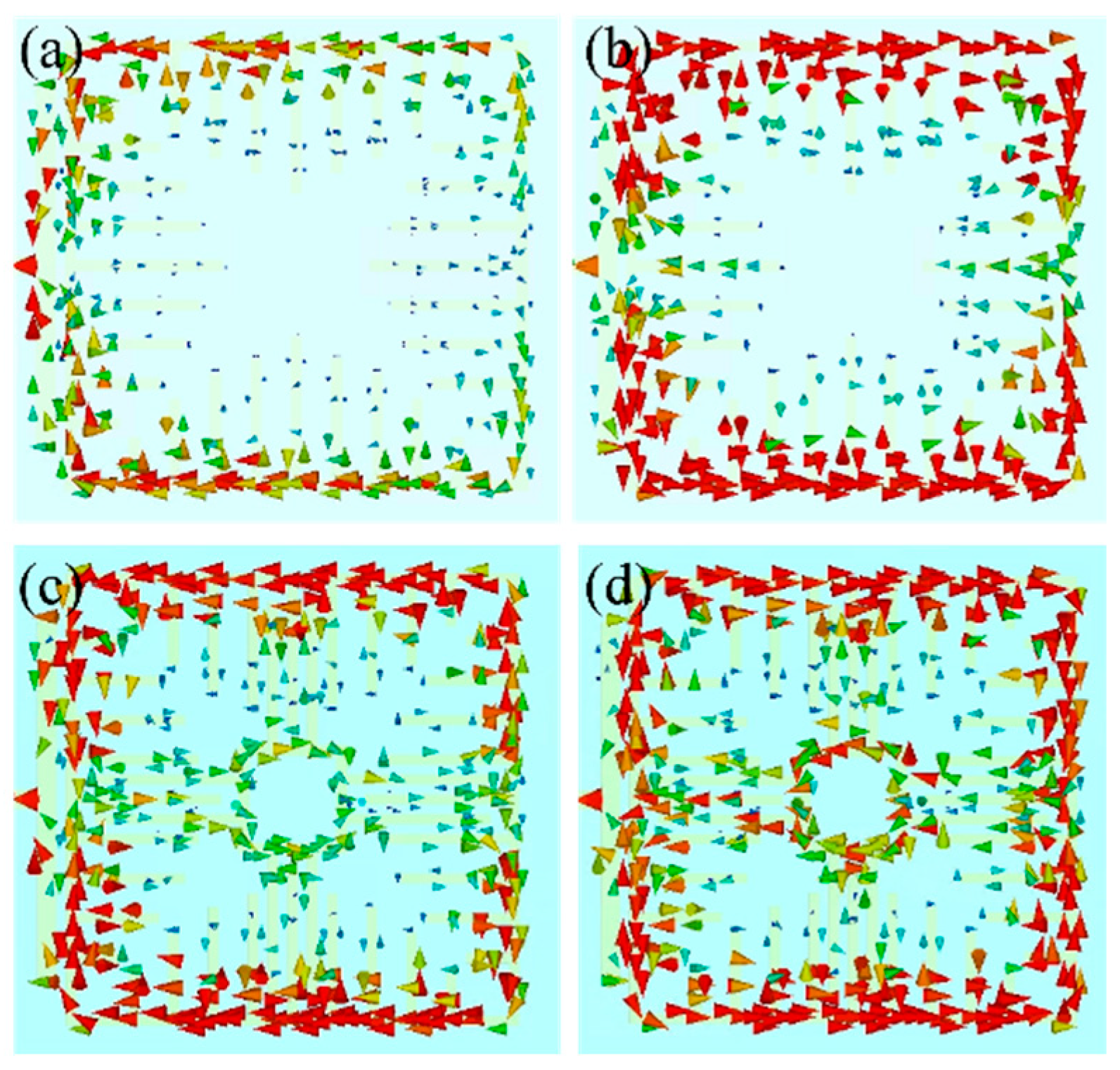
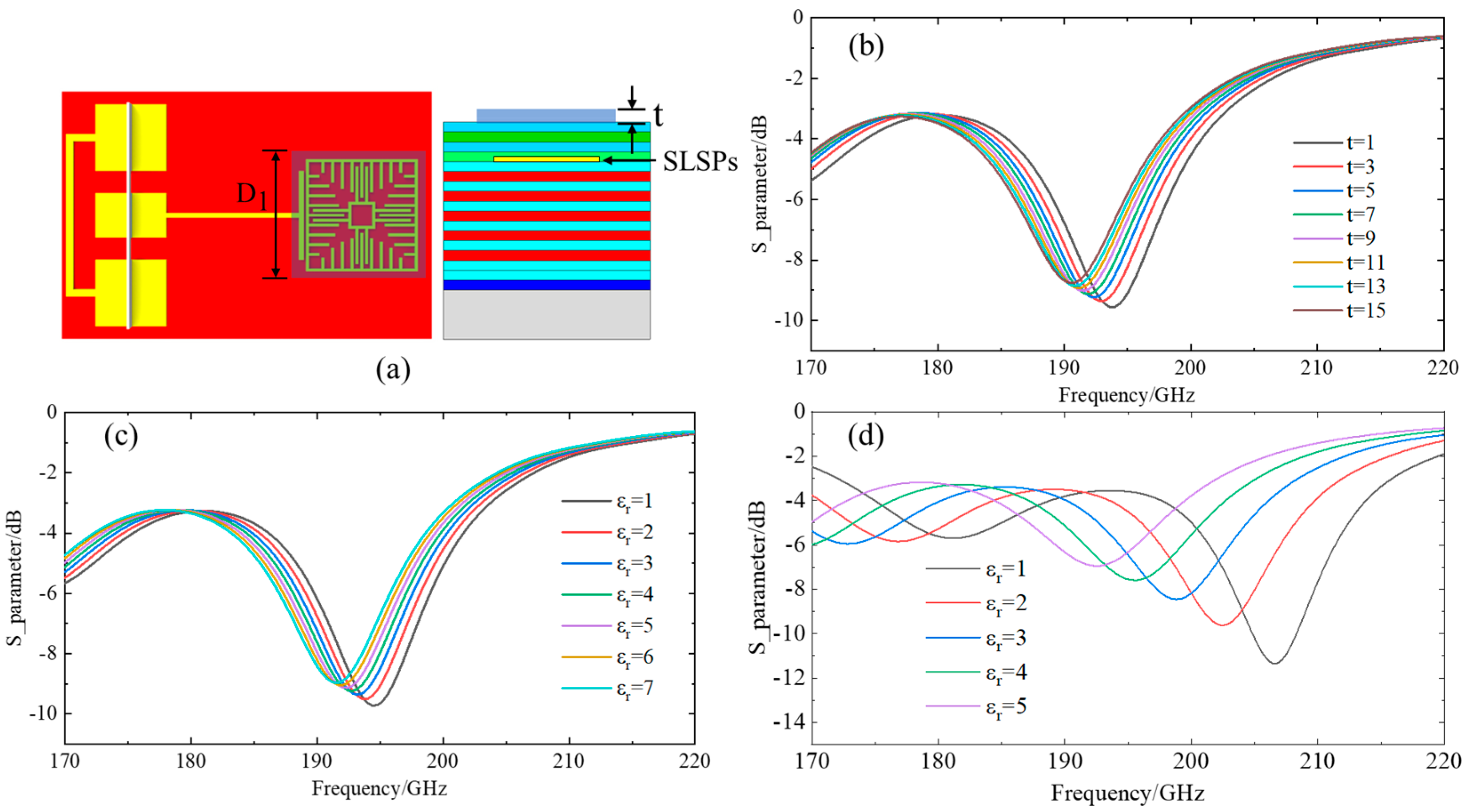
2. Designs and Simulations

To investigate the characteristics of the hybridized SLSP resonator, we firstly simulated the cavity SLSP resonator for comparison. As illuminated in Figure 1, the cavity resonator has a regular quadrilateral structure, with metallic spokes arranged periodically around the resonator. The attached spokes are located inside the cavity and extend inward. On one side of the cavity resonator, the length of the attached spokes decreases gradually from the middle to both sides. And the resonator is fed by a non-contact coupling excitation, which is composed of a microstrip line terminated by a stub. A ground–signal–ground (GSG) pad is positioned on the left of the excitation to connect the external terahertz signal. Moreover, the non-contact coupling excitation exerts the role of a probe, which can excite the resonance of SLSP through an evanescent field [29]. By tuning the length of the terminal stub L 1 and the gap between the resonator and the stub, the coupling efficiency of the feeding could be adjusted effectively.
Figure 2 shows the cross section of the CMOS technology, which provides six metal layers (ML1–ML6) for flexible design. ML2 is chosen for metal ground with a thickness of 0.53 μ m . The thickness of ML6 (4.6 μ m ) is the largest among the metal layers, which offers the advantage of reducing loss. Therefore, ML6 is selected to design the SLSP. Both the SLSP resonator and ground are made of copper. And the dielectric properties of the CMOS technology are listed in Table 1.
An electromagnetic full-wave simulation was performed using CST Studio Suite with the finite integration technique, as depicted in Figure 3. The boundary condition is set as open add space in all directions. With the time domain solver, the cavity SLSP resonator was simulated to obtain the reflection coefficient, as well as the E z -field distributions on the xoy plane. In Figure 3a, two obvious resonances labeled m1 and m2 are observed at 173.6 GHz and 234 GHz, corresponding to the E z -field distributions on the xoy plane presented in Figure 3b,c. From the E z -field distribution, mode m1 could be categorized as asymmetric mode, when mode m2 is a dipole mode, demonstrating that SLSP resonant mode is successfully excited. In particular, the Q-factor of mode m2 can be calculated by the following equation:
Q = f 0 f 3 d B
where f 0 is the center frequency, and f 3 d B is the 3 dB bandwidth. The Q-factor of the dipole mode is 53.
Then, a core SLSP resonator was incorporated inside the cavity SLSP resonator to form the hybridized SLSP resonator, as shown in Figure 4. The shape of the core SLSP resonator is also regular quadrilateral, the same as the cavity resonator. And spokes attached outside the metallic quadrilateral of core resonator interdigitate with the spokes on the cavity resonator. According to our previous work [28], strong coupling between interdigitated spokes will be generated. By altering the length of the spokes, the resonant characteristics will be changed accordingly. Figure 5a illustrates the S parameter of hybridized SLSP resonator in comparison to the cavity resonator. Two resonant modes of the hybridized resonator are observed and labeled M1 and M2, which are located at 168.8 GHz and 194.4 GHz, respectively. Compared with the cavity resonator, both resonant modes of hybridized resonator exhibit red shifts, indicating the ability to reduce the electric size of the resonator. In Figure 5b,c, the electric field distributions of modes M1 and M2 are presented, revealing that the cavity and core resonators resonate out-phase.
To study the resonance modes in detail, the surface currents of modes m1, m2, M1, M2 were monitored and are plotted in Figure 6. The surface current of the cavity SLSP resonator are shown in Figure 6a,b. It can be observed that there are a pair of surface currents around the periphery of the cavity resonator, corresponding to the electric field oscillated out-phase of modes m1 and m2. In comparison, two pairs of surface currents oscillated out-phase are also observed around the hybridized SLSP structure. In Figure 6c,d, a pair of surface currents flow around the cavity resonator while another pair of currents flow around the core resonator. The overlapping of the currents increases the current path, which makes the red shift occur. In particular, the surface current intensity around the core resonator of mode M2 is stronger than that of mode M1, resulting in a more significant red shift in mode M2.

3. Sensing Simulation

A sensing analysis was performed to reveal the potential of the proposed SLSP resonator as a sensor chip. A dielectric film was placed on top of the resonator, and then the S parameter spectra were obtained by varying the design parameters of the film, as shown in Figure 7a–d. The sensing figure of merit (FoM) is commonly employed to evaluate the performance of a sensor, and it is calculated by the following equation:
F o M = s e n s i t i v i t y Δ f 3 d B  
where s e n s i t i v i t y = Δ f / Δ n , n = ε r , and ε r is the relative permittivity of the dielectric film. Considering the high Q-factor of mode M2, the simulation frequency band was narrowed to 170–220 GHz. When t = 15 μ m , ε r changed from 1 to 10, and the resonance frequency of mode M2 shifted from 194.4 GHz to 191.6 GHz. Based on the results above, the F o M and s e n s i t i v i t y of mode M2 were calculated. The F o M of mode M2 was 0.22 RIU−1, while the s e n s i t i v i t y of mode M2 was 1.7 GHz·RIU−1. On the one hand, the thickness of the film could affect the frequency shift of mode M2. On the other hand, due to the existence of the pass layers, the interaction between the dielectric film and the SLSP resonator was reduced, resulting in a limited sensing performance.
Figure 7b shows the influence of thickness on the frequency shift. It can be observed that a thicker film resulted in a greater frequency shift. Hence, it is appropriate to design a tested sample as thick as possible to improve the sensitivity in the experiment. Furthermore, Figure 7d shows the sensing performance of the chip without pass layers. When t = 15 μ m , ε r varied from 1 to 5, the sensitivity of the proposed resonator could be calculated as 11 GHz·RIU−1, and the FoM was 1.87 RIU−1, both of which presented a significant improvement compared to the original chip. In future designs, on-chip technology without pass layers will be investigated for a further enhancement of sensing performance.

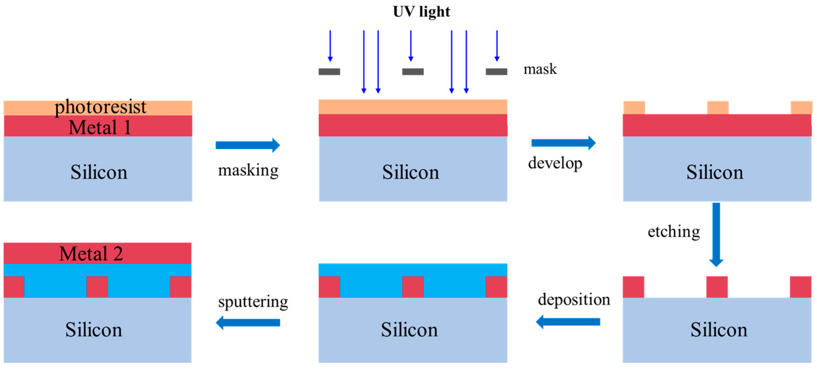
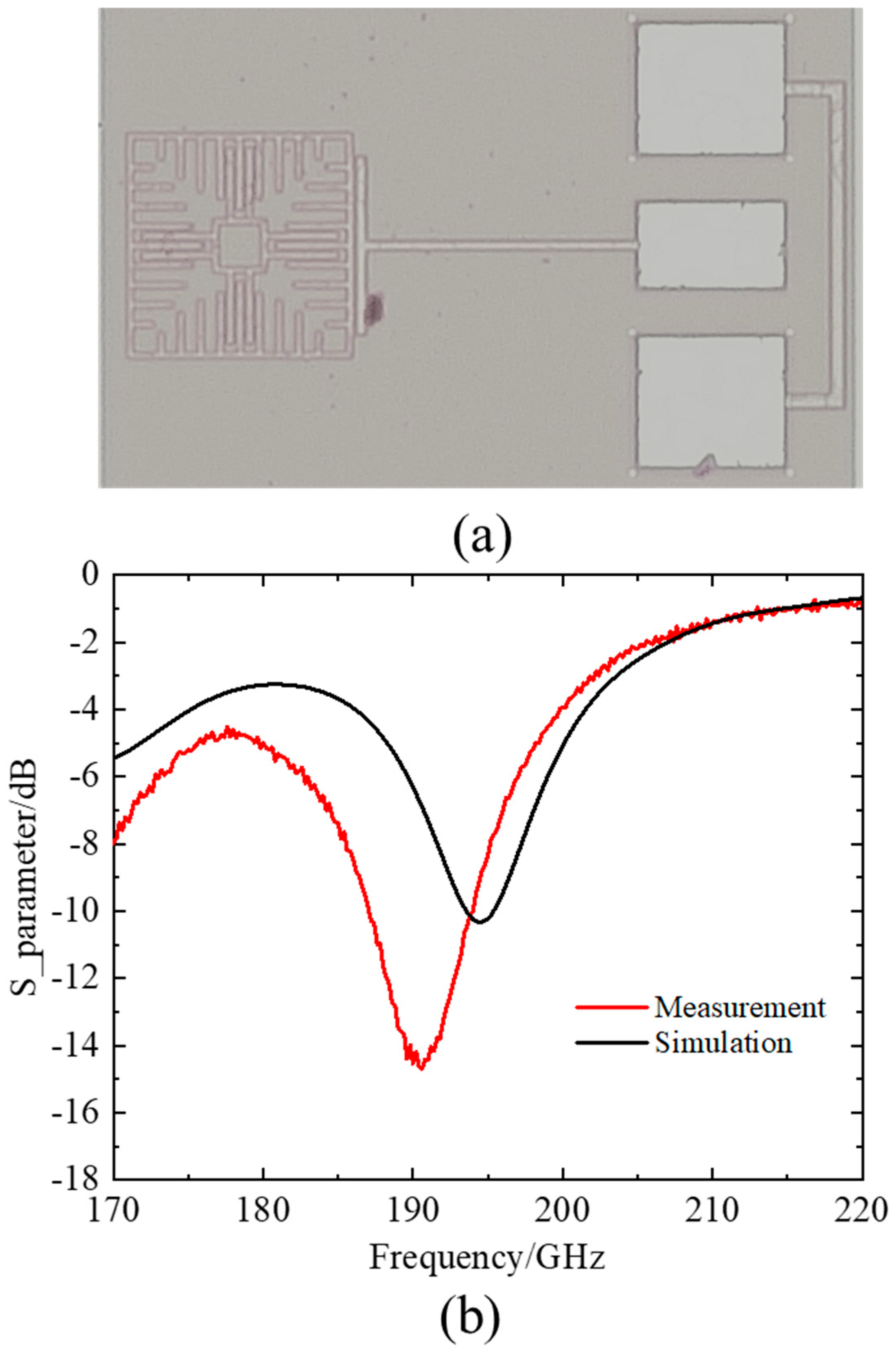
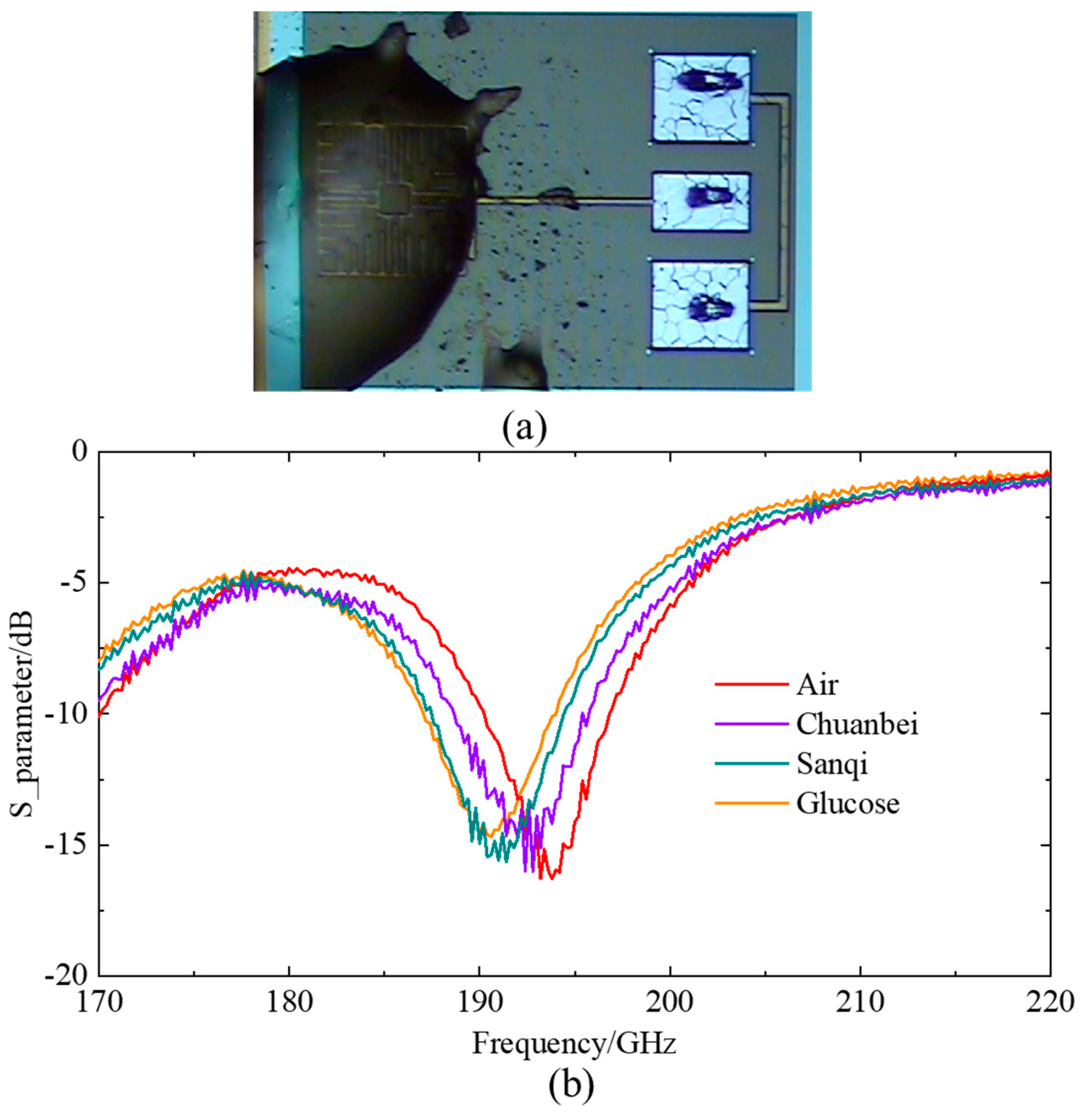
4. Experimental Results

The proposed resonator was fabricated utilizing 0.18 μ m CMOS technology, with the fabrication processes illustrated in Figure 8. Firstly, a metal layer was grown on the silicon substrate by physical vapor deposition (PVD), and then photoresist was spun onto metal 1. After exposing the photoresist to UV light with a mask and removing the unnecessary photoresist, the designed structure was developed by the remaining photoresist. Next, an etching process was conducted to pattern the metal 1. Subsequently, a substrate was deposited on the metal 1 layer, and the next metal layer was sputtered on the substrate. The fabricated SLSP resonator is depicted in Figure 9a.
Complete S parameters from 170 GHz to 220 GHz were measured by the VectorStar broadband vector network analyzer ME7838G. The comparison between the simulation result and the measured result is presented in Figure 9b. The simulation and experimental results are located at 194.4 GHz and 194 GHz, respectively, with quite a small frequency deviation. The measured Q-factor was 56.7, which was higher than the simulated one. Due to the limitation in simulation accuracy of CST, the simulated results were not capable of capturing the exact Q-factor, particularly for high Q-factor structures [25,26]. And as the frequency increases, the deviation between simulation and experiment will also increase accordingly. Furthermore, fabrication and experiment tolerance will influence the measured result as well, which might lead to an experiment result better than the simulated result.
To verify the highly sensitive biosensing properties of the SLSP sensor, a series of experimental verifications were conducted for medicinal solution sensing. Three medicinal powders were made into solutions for the experiment: Sanqi, Chuanbei, and glucose. Figure 9a presents the fabricated chip, and Figure 10a shows the operation of the sensing experiment with a solution dripped on the SLPSs. After each solution measurement was completed, the chip was cleaned by an ultrasonic cleaner. After the last solution was cleaned off, the chip was dried thoroughly in air. Subsequently, the next solution was dripped onto the chip, and the measurement was conducted after the solution dried into a film. The process was repeated until the experiment was completed. All the measurements were carried out under room temperature, and the humidity was the same as the environment.
The measured S parameter spectra are shown in Figure 10b. It can be observed that compared to the S parameter in air, the spectra under tested samples exhibit a significant red shift, while maintaining a high Q-factor. Compared to air, the frequency shift for Chuanbei was 1.4 GHz, and the one for Sanqi was 3.2 GHz, whereas the one for glucose was 4 GHz. The emergence of frequency shifts with different samples demonstrates the potential of the resonator as a promising candidate for a variety of terahertz sensing applications.
Here, the concentrations of the solutions were challenging to control because the powders could not be dissolved in water completely. Therefore, the experiment results provide a qualitative analysis for biosensing without accurate information of the samples under test. In the future, quantitative measurements will be explored and implemented. For example, extracts of medicines can be adopted, which could be dissolved in water perfectly, and a microfluidic channel can be elaborately designed on the chip for quantitative analysis, allowing for the evaluation of sensing FoM.
To highlight the superior features of the proposed SLSP, a comparison between this work and state-of-the-art resonators are listed in Table 2. In ref. [13], the proposed resonator showed a small electric size, but the Q-factor was reduced to 16.7. In ref. [26], although the Q-factor of the proposed resonator reached 49, the electrical size was as large as 0.96λ × 0.96λ. Compared to the resonator proposed in refs. [13,26], the proposed hybridized SLSP resonator shows a smaller electrical size of 0.081λ × 0.081λ, and a higher Q-factor of 56.7, exhibiting a great superiority of the hybridized structure.

5. Conclusions

In this work, a novel approach is presented for achieving a high Q-factor compact resonator utilizing CMOS technology, based on the spoof localized surface plasmons. A quadrilateral hybridized SLSP resonator is proposed and fabricated with a compacted electric size of 0.081λ × 0.081λ. The measured Q-factor was as high as 56.7 in the THz frequency range. Pharmaceutical testing was also implemented on three medicine solutions: Sanqi, Chuanbei, and glucose, and frequency shifts of 1.4 GHz, 3.2 GHz, and 4 GHz were observed. The hybridized SLSP resonator provides a new solution for CMOS high-sensitivity sensor in the terahertz band.

Author Contributions

Conceptualization, D.B.; methodology, C.L.; software, M.W. and C.L.; validation, M.W., C.L. and J.W.; investigation, K.L.; resources, H.G.; data curation, Z.Q.; writing—original draft preparation, M.W.; writing—review and editing, D.B. All authors have read and agreed to the published version of the manuscript.

Funding

This research was funded by the National Key Research and Development Program (Grant No. 2023YFB3811300, 2023YFB3811302); and the 111 Project (Grant No. 111-2-05).

Data Availability Statement

Dataset available on request from the authors.

Acknowledgments

M.W., C.L. and D.B. contributed equally to this work. The authors wish to thank Meng Zhang for critical guidance.

Conflicts of Interest

The authors declare no conflicts of interest.

References

  1. Qin, J.; Jiang, S.; Wang, Z.; Cheng, X.; Li, B.; Shi, Y.; Tsai, D.P.; Liu, A.Q.; Huang, W.; Zhu, W. Metasurface Micro/Nano-Optical Sensors: Principles and Applications. ACS Nano 2022, 16, 11598–11618. [Google Scholar] [CrossRef] [PubMed]
  2. Owji, E. 2D Materials Coated on Etched Optical Fibers as Humidity Sensor. Sci. Rep. 2021, 11, 1771. [Google Scholar] [CrossRef] [PubMed]
  3. Xu, Y.; Bai, P.; Zhou, X.; Akimov, Y.; Png, C.E.; Ang, L.-K.; Knoll, W.; Wu, L. Optical Refractive Index Sensors with Plasmonic and Photonic Structures: Promising and Inconvenient Truth. Adv. Opt. Mater. 2019, 7, 1801433. [Google Scholar] [CrossRef]
  4. Shin, J.; Liu, Z.; Bai, W.; Liu, Y.; Yan, Y.; Xue, Y.; Kandela, I.; Pezhouh, M.; MacEwan, M.R.; Huang, Y.; et al. Bioresorbable Optical Sensor Systems for Monitoring of Intracranial Pressure and Temperature. Sci. Adv. 2019, 5, eaaw1889. [Google Scholar] [CrossRef] [PubMed]
  5. Su, J.; Goldberg, A.F.; Stoltz, B.M. Label-Free Detection of Single Nanoparticles and Biological Molecules Using Microtoroid Optical Resonators. Light Sci. Appl. 2016, 5, e16001. [Google Scholar] [CrossRef]
  6. Prabowo, B.; Purwidyantri, A.; Liu, K.-C. Surface Plasmon Resonance Optical Sensor: A Review on Light Source Technology. Biosensors 2018, 8, 80. [Google Scholar] [CrossRef]
  7. Zhang, X.; Cui, W.Y.; Lei, Y.; Zheng, X.; Zhang, J.; Cui, T.J. Spoof Localized Surface Plasmons for Sensing Applications. Adv. Mater. Technol. 2021, 6, 2000863. [Google Scholar] [CrossRef]
  8. Liao, Z.; Liu, S.; Ma, H.F.; Li, C.; Jin, B.; Cui, T.J. Electromagnetically Induced Transparency Metamaterial Based on Spoof Localized Surface Plasmons at Terahertz Frequencies. Sci. Rep. 2016, 6, 27596. [Google Scholar] [CrossRef] [PubMed]
  9. Liang, Y.; Yu, H.; Zhang, H.C.; Yang, C.; Cui, T.J. On-Chip Sub-Terahertz Surface Plasmon Polariton Transmission Lines in CMOS. Sci. Rep. 2015, 5, 14853. [Google Scholar] [CrossRef]
  10. Shang, Y.; Yu, H.; Hu, S.; Liang, Y.; Bi, X.; Arasu, M.A. High-Sensitivity CMOS Super-Regenerative Receiver with Quench-Controlled High-$Q$ Metamaterial Resonator for Millimeter-Wave Imaging at 96 and 135 GHz. IEEE Trans. Microw. Theory Technol. 2014, 62, 3095–3106. [Google Scholar] [CrossRef]
  11. Gao, X.; Chen, B.J.; Shum, K.; Ma, Q.; Cui, W.Y.; Cui, T.J.; Chan, C.H. Multifunctional Terahertz Spoof Plasmonic Devices. Adv. Mater. Technol. 2023, 8, 2202050. [Google Scholar] [CrossRef]
  12. Zhang, H.C.; Zhang, Q.; Liu, J.F.; Tang, W.; Fan, Y.; Cui, T.J. Smaller-Loss Planar SPP Transmission Line than Conventional Microstrip in Microwave Frequencies. Sci. Rep. 2016, 6, 23396. [Google Scholar] [CrossRef] [PubMed]
  13. Dong, G.; Shen, Y.; Hu, S. On-Chip Localized Surface Plasmon Resonator for 127 GHz Compact CMOS Oscillator. IEEE Electron Device Lett. 2023, 44, 1927–1930. [Google Scholar] [CrossRef]
  14. Thapa, S.K.; Pokharel, R.K.; Chen, B.; Barakat, A. On-Chip Millimeter-Wave DGS Based Bandstop Filter in 0.18-μm CMOS Process. IEEE Trans. Circuits Syst. II 2022, 69, 2732–2736. [Google Scholar] [CrossRef]
  15. Harmankaya, S.; Deveci, H.A.; Harmankaya, A.; Gül, F.H.; Atar, N.; Yola, M.L. Thiram Determination in Milk Samples by Surface Plasmon Resonance Based on Molecularly Imprinted Polymers and Sulphur-Doped Titanium Dioxide. Biosensors 2024, 14, 329. [Google Scholar] [CrossRef] [PubMed]
  16. Pesavento, M.; Zeni, L.; Maria, L.D.; Alberti, G.; Cennamo, N. SPR-Optical Fiber-Molecularly Imprinted Polymer Sensor for the Detection of Furfural in Wine. Biosensors 2021, 11, 72. [Google Scholar] [CrossRef]
  17. Pors, A.; Moreno, E.; Martin-Moreno, L.; Pendry, J.B.; Garcia-Vidal, F.J. Localized Spoof Plasmons Arise While Texturing Closed Surfaces. Phys. Rev. Lett. 2012, 108, 223905. [Google Scholar] [CrossRef] [PubMed]
  18. Liao, Z.; Luo, Y.; Fernández-Domínguez, A.I.; Shen, X.; Maier, S.A.; Cui, T.J. High-Order Localized Spoof Surface Plasmon Resonances and Experimental Verifications. Sci. Rep. 2015, 5, 9590. [Google Scholar] [CrossRef] [PubMed]
  19. Gholamian, M.; Shabanpour, J.; Cheldavi, A. Highly Sensitive Quarter-Mode Spoof Localized Plasmonic Resonator for Dual-Detection RF Microfluidic Chemical Sensor. J. Phys. D Appl. Phys. 2020, 53, 145401. [Google Scholar] [CrossRef]
  20. Zhang, X.; Cui, T.J. Contactless Glucose Sensing at Sub-Micromole Level Using a Deep-Subwavelength Decimeter-Wave Plasmonic Resonator. Laser Photonics Rev. 2022, 16, 2200221. [Google Scholar] [CrossRef]
  21. Luo, C.; Chen, L. Highly Sensitive and Tunable Absorption-Induced Transparency for Terahertz Fingerprint Sensing with Spoof Surface Plasmon Polaritons. IEEE Sens. J. 2024, 24, 17686–17692. [Google Scholar] [CrossRef]
  22. Yang, B.J.; Zhou, Y.J.; Xiao, Q.X. Spoof Localized Surface Plasmons in Corrugated Ring Structures Excited by Microstrip Line. Opt. Express OE 2015, 23, 21434–21442. [Google Scholar] [CrossRef]
  23. Liao, Z.; Pan, B.C.; Shen, X.; Cui, T.J. Multiple Fano Resonances in Spoof Localized Surface Plasmons. Opt. Express 2014, 22, 15710. [Google Scholar] [CrossRef] [PubMed]
  24. Shen, X.; Cui, T.J. Ultrathin Plasmonic Metamaterial for Spoof Localized Surface Plasmons: Spoof Localized Surface Plasmons. Laser Photonics Rev. 2014, 8, 137–145. [Google Scholar] [CrossRef]
  25. Kim, Y.; Salim, A.; Lim, S. Millimeter-Wave-Based Spoof Localized Surface Plasmonic Resonator for Sensing Glucose Concentration. Biosensors 2021, 11, 358. [Google Scholar] [CrossRef]
  26. Zhou, J.; Chen, L.; Sun, Q.; Liao, D.; Ding, L.; Balakin, A.V.; Shkurinov, A.P.; Xie, J.; Zang, X.; Cheng, Q.; et al. Terahertz On-Chip Sensing by Exciting Higher Radial Order Spoof Localized Surface Plasmons. Appl. Phys. Express 2020, 13, 012014. [Google Scholar] [CrossRef]
  27. Wang, J.; Zhang, J.; Gao, H.; Fu, X.; Bao, D.; Cui, T.J. Mixed-Resolution High-Q Sensor Based on Hybridized Spoof Localized Surface Plasmons. Front. Phys. 2022, 10, 850186. [Google Scholar] [CrossRef]
  28. Bao, D.; Cheng, Q.; Jiang, W.X.; Zhang, J.J.; Liao, Z.; Wu, J.W.; Yang, J.; Zhang, X.R.; Cui, T.J. Concentric Designer Plasmon Hybridization in Deep Subwavelength Metamaterial Resonator. Appl. Phys. Lett. 2019, 115, 121103. [Google Scholar] [CrossRef]
  29. Su, H.; Shen, X.; Su, G.; Li, L.; Ding, J.; Liu, F.; Zhan, P.; Liu, Y.; Wang, Z. Efficient Generation of Microwave Plasmonic Vortices via a Single Deep-Subwavelength Meta-Particle. Laser Photonics Rev. 2018, 12, 1800010. [Google Scholar] [CrossRef]
Figure 1. Schematic of the cavity SLSP resonator, in which D = 126 μ m , l 1 = 40 μ m , l 2 = 34 μ m , l 3 = 30 μ m , l 4 = 23 μ m , l 5 = 12 μ m , g a p 1 = 8 μ m , and L = 150 μ m .
Photonics 12 00102 g001
Figure 2. Cross section of the CMOS technology.
Photonics 12 00102 g002
Figure 3. (a) The simulated reflection coefficient. (b,c) The E z −field distributions of the cavity SLSP structure.
Photonics 12 00102 g003
Figure 4. Schematic of the hybridized LSP resonator structure.
Photonics 12 00102 g004
Figure 5. (a) The simulation results comparison of the hybridized SLSP resonator and the cavity resonator. (b,c) The electric field distributions of modes M1 and M2.
Photonics 12 00102 g005
Figure 6. Surface current distributions of modes (a) m1, (b) m2, (c) M1, and (d) M2.
Photonics 12 00102 g006
Figure 7. (a) The proposed SLSP resonator under dielectric film for sensing simulation, D 1 = 146 μ m . (b,c) S parameter obtained from changing t and ε r . (d) Simulation sensing performance without pass layers.
Photonics 12 00102 g007
Figure 8. Process flow of CMOS technology.
Photonics 12 00102 g008
Figure 9. (a) The microscopic image of the proposed SLSP. (b) Comparison of measured and simulated S parameter.
Photonics 12 00102 g009
Figure 10. (a) The microscopic image of fabricated sample during sensing experiment. (b) The measured results for the sensing experiment.
Photonics 12 00102 g010
Table 1. Design parameters of the CMOS technology.
DielectricThickness (μm)Relative Permittivity
PASS30.67.9
PASS20.154.15
PASS13.64.15
DIEL_METAL64.73.8
DIEL_CTM_VIA0.883.83
IMD5A0.553.7
IMD (4A-1A)0.6153.7
DIEL_VIA (4-1)0.7653.819
ILD20.54
ILD10.254
FOX0.353.9
Table 2. Comparison between this work and state-of-the-art resonators.
Ref.Frequency
(GHz)
Physical SizeElectrical SizeQ-Factor
[13]614.558 μm × 67 μm0.12λ × 0.14λ16.7
[26]166.5860 μm × 860 μm0.96λ × 0.96λ49
This work194126 μm × 126 μm0.081λ × 0.081λ56.7
Disclaimer/Publisher’s Note: The statements, opinions and data contained in all publications are solely those of the individual author(s) and contributor(s) and not of MDPI and/or the editor(s). MDPI and/or the editor(s) disclaim responsibility for any injury to people or property resulting from any ideas, methods, instructions or products referred to in the content.

