Article

Design of a Tunable Metamaterial Absorption Device with an Absorption Band Covering the Mid-Infrared Atmospheric Window

1
Yunnan Radioactive Environment Supervision Station, Kunming 650093, China
2
Faculty of Materials Science and Engineering, Kunming University of Science and Technology, Kunming 650093, China
3
College of Physics, Central South University, Changsha 410083, China
*
Authors to whom correspondence should be addressed.
Photonics 2025, 12(2), 148; https://doi.org/10.3390/photonics12020148
Submission received: 31 December 2024 / Revised: 6 February 2025 / Accepted: 10 February 2025 / Published: 12 February 2025
(This article belongs to the Special Issue Photonics Metamaterials: Processing and Applications)

Abstract

:
We propose a highly efficient broadband tunable metamaterial infrared absorption device. The design is modeled using the three-dimensional finite element method for the absorption device. The results show that the absorption device captures over 90% of the light in the wavelength range from 6.10 μm to 17.42 μm. We utilize VO2’s phase change property to adjust the absorption device, allowing the average absorption level to vary between 20.61% and 94.88%. In this study, we analyze the electromagnetic field distribution of the absorption device at its peak absorption point and find that the high absorption is achieved through both surface plasmon resonance and Fabry–Perot cavity resonance. The structural parameters of the absorption device are fine-tuned through parameter scanning. By comparing our work with previous studies, we demonstrate the superior performance of our design. Additionally, we investigate the polarization angle and incident angle of the absorption device and show that it is highly insensitive to these factors. Importantly, the simple structure of our absorption device broadens its potential uses in photodetection, electromagnetic stealth, and sensing.

1. Introduction

Infrared is one of the invisible rays of the sun and is also an electromagnetic wave [1,2]. It has a lower frequency than visible light and is also known as infrared radiation. Since its discovery by Herschel in 1800, infrared radiation has been studied continuously. In later studies, it has been found that infrared radiation can interact with many molecules and show strong heating effects at the large scale [3]. Moreover, infrared radiation has three atmospheric windows [4,5,6]. Water vapor, CO2, and ozone in the Earth’s atmosphere absorb electromagnetic waves, and the electromagnetic band with a higher transmission rate is called the atmospheric window [7,8]. This part of infrared radiation that passes through the atmosphere to reach the Earth has a big impact on human activities. The question of how to control this part of electromagnetic waves has gained much attention. Initially, researchers used the natural properties of materials to modulate this part of electromagnetic waves, but this method has many drawbacks such as narrow bandwidth, low efficiency, and large size [9,10]. This has become the main problem limiting the control of infrared electromagnetic waves. With the improvement of manufacturing processes, the materials studied are no longer limited to natural materials, but efforts are made to create materials that do not exist in nature to achieve electromagnetic control [11]. Such artificial materials are called metamaterials [12,13,14].
Metamaterials are materials with special structures and specific designs with sub-wavelength unit scales that are capable of modifying or controlling the behavior of electromagnetic radiation in a very significant way [15]. They allow energy such as light, sound, and electromagnetic waves to interact with the material in an extraordinary way through their carefully designed structures. Metamaterials have witnessed tremendous progress over the past few decades, capturing widespread interest owing to their extraordinary properties and vast potential for diverse applications [16,17,18]. Metamaterials often exhibit unconventional properties such as reverse refraction, negative refraction, negative refractive indexes, and superscattering. Among them, a metamaterial absorption device is a metamaterial-based device that is characterized by a high absorption capacity for electromagnetic waves in a specific frequency range. This device utilizes a combination of the special structure of the metamaterial and the wave-absorbing material to effectively capture and absorb electromagnetic radiation at specific wavelengths. The operating principle of metamaterial absorption devices involves microscopic elements in their structure, such as micro- and nanostructures or electromagnetic resonators [19,20,21]. They achieve the efficient absorption of electromagnetic waves by tuning the electromagnetic response of the material. By rationally designing the structural parameters and material composition of metamaterial absorption devices, the selective absorption and suppression of electromagnetic waves in specific frequency bands can be realized [22]. Metamaterial absorption devices have a wide range of application prospects. Researchers have now applied metamaterials to electromagnetic stealth [23], biosensors [24], energy harvesting [25], and so on. However, by reviewing the previous studies, we find that there are fewer studies on metamaterial absorbers with absorption bands covering the infrared atmospheric window. And most of the metamaterial infrared absorbers have a narrow absorption bandwidth and the absorption characteristics are not tunable [26,27]. Therefore, the design of a metamaterial absorber with a broadband absorption band covering the infrared atmospheric window and with an adjustable absorption rate is extremely promising. Regarding the tuning of the absorption rate, we use phase change materials for this purpose. Phase change materials are a special type of material that can exhibit dramatic changes in physical properties in response to changes in temperature, pressure, or other external conditions [28,29]. Such materials can change rapidly from one phase to another, for example, from solid to liquid, liquid to gas, or vice versa. The special feature of phase change materials is that the phase change process is accompanied by a large amount of heat absorption or exothermic phenomena and that the energy required for the phase change is relatively small. This means that phase change materials have an efficient ability to store and release energy when absorbing or releasing energy. This property gives phase change materials the potential for a wide range of applications in many fields. Based on this, we have investigated and proposed a mid-infrared metamaterial absorption device. At an elevated temperature of 342 K, it achieves seamless absorption of over 90% across the eloquent 6.10 μm to 17.42 μm (11.32 μm) spectrum, boasting an average absorption efficacy of 94.88%. It is obvious that the operating band of our designed absorption device contains the mid-infrared band atmospheric window (8–14 μm). Not only that, but our absorption device also has tunable absorption. Its average absorption rate in the working band can be tuned within 20.61–94.88%. It is well known that the sensitivity to the polarization angle and incidence angle of electromagnetic waves has a non-negligible effect on optoelectronic devices. Through the study, we found that our designed absorption device has good insensitivity to polarization angle and incidence angle. Not only that, but the absorption device we designed also only has a three-layer structure, which is easy to fabricate. Therefore, it has more application potential in infrared stealth, optoelectronic detection, and energy harvesting. At the same time, this tunable absorption device designed by us is also more capable of meeting the application requirements in different scenarios. This study used a general analytical approach and only explored the absorption effect of the absorber device. We can also use fractional heat transport models to enhance the analysis of transient heat dissipation in infrared absorbing devices. For example, the modified Caputo fractional derivative can capture the memory effect in thermal diffusion, especially under pulsed laser irradiation. Furthermore, the size-dependent thermal conductivity observed in 2D materials suggests that the fractional model may be useful for optimizing nanostructured absorber layers with controlled defects. Moreover, the fractional heat transport model has many applications, not only in the thermal management of infrared absorbers, but it also has advantages in material design and thermal transport modulation. In future studies, the use of fractional heat transport models will be focused on to increase the depth of the work.

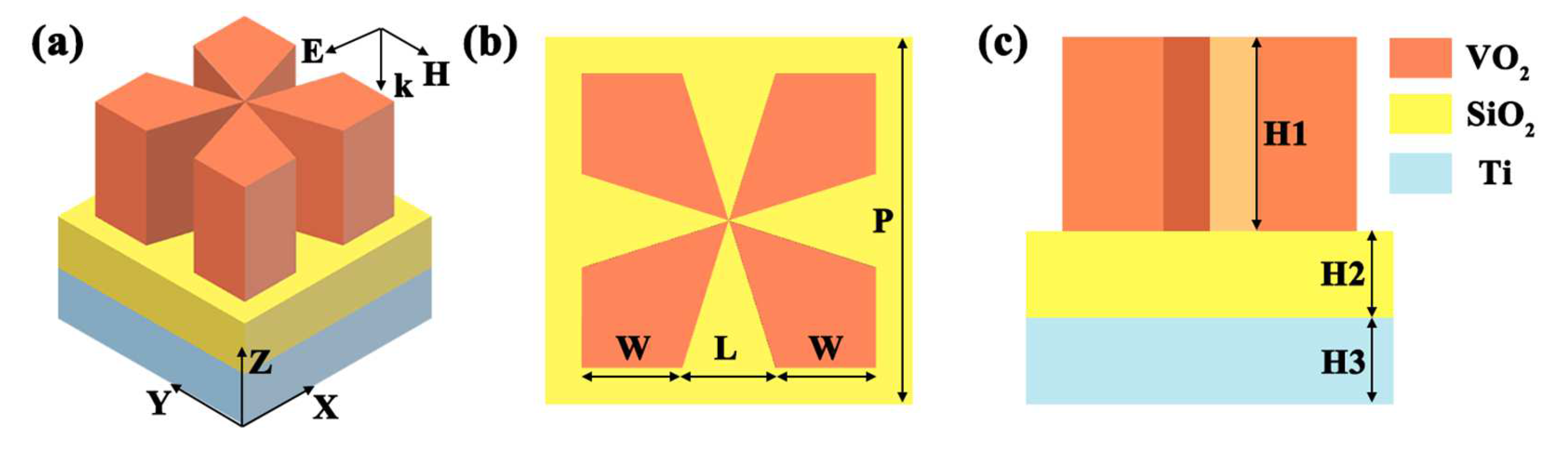
2. Structural Design and Parameters

In this endeavor, we have crafted a metamaterial infrared absorption device apparatus with a flexibly adjustable absorption capacity that spans the mid-infrared atmospheric range from 8 μm to 14 μm. We used FDTD solutions simulation software (Lumerical FDTD Solutions 2020) for simulation. The absorption device’s structure is shown in Figure 1. Our proposed absorption device is a three-layer structure. Its bottom layer is a titanium substrate. The middle layer is a silica dielectric layer. The top layer is a dart-shaped VO2 resonator layer. VO2 undergoes a reversible phase transition from the insulating to the metallic state at ~68 °C, which significantly alters its optical and electrical properties. The tunable absorption of electromagnetic waves can be achieved using its phase transition properties. Moreover, in the infrared band, VO2 can effectively absorb infrared radiation at specific wavelengths, thus achieving efficient infrared absorption. Titanium, with its high reflectivity, is used as a substrate material to enhance the overall performance of the IR absorption device. SiO2, with its low refractive index, is used as a dielectric layer to reduce the reflection loss of the incident light, thus improving the absorption efficiency. In Figure 1, H3 is the thickness of the titanium substrate, H2 is the thickness of the middle SiO2 layer, H1 is the thickness of the top VO2 layer, P is the period length of the absorber unit structure, L is the horizontal distance between two adjacent dart edges of the dart-shaped VO2 structure, and W is the length of each dart edge. Specific values for these structural parameters are given in Table 1.
The effect of the variation in these structural parameters on the absorption device will be specifically analyzed subsequently. The modulation of our designed absorption device is mainly realized through the dart-like VO2 layer. This is because the substance VO2 has a phase change effect [30]. At temperatures below 340 K, VO2 exhibits a monoclinic crystalline phase in the insulating state. At a temperature of 340 K, VO2′s phase transition temperature starts to transform from a monoclinic phase to a tetragonal phase in the metal state. At a temperature of 342 K, VO2 transforms to the metal state completely. During the phase transition of VO2, its conductivity changes. Therefore, we can realize the regulation of the absorption rate by changing the temperature and thus the conductivity of VO2. The insulating component in the VO2 used in the design can be understood as a dielectric with dielectric constant ε D = 9 . For the metal component in VO2, the dielectric constant can be expressed using the Drude model as shown in Equation (1) [31,32] as follows:
ε M ( ω , σ ) = ε ω P 2 ( σ ) ω ( ω + i / τ )
where ω is the frequency of the infrared radiation. ε is the high-frequency limiting dielectric constant with a value of 12. τ is the relaxation time, which can be described using Equation (2). ω P ( σ ) is the plasma frequency, and the value at σ can be expressed using Equation (3). Equations (2) and (3) are expressed as follows:
τ = m * μ e
ω P ( σ ) = Ne 2 ε 0 m *
In Equation (2), m * = 2 m e is the effective mass. m e is the mass of the free electron. μ is the carrier mobility and is 2   cm 3 / V S . e is the charge of the free electron. Thus, τ = 2.2 fs . In Equation (3) N is the carrier concentration inside the VO2 medium, noted as 8.7 × 10 21 cm 3 . ε 0 is the dielectric constant in vacuum. In addition, the volume fraction f of the metal component in VO2 versus temperature can be described by the Boltzmann function, as shown in Equation (4) as follows:
f = f max 1 1 1 + exp ( T T 0 ) / Δ T
Here, f max = 0.95 is the maximum value that can be reached by the volume fraction of the metal component in VO2 [33]. T 0 = 68   C is the critical temperature of the phase transition at elevated temperatures of VO2, which corresponds to the critical temperature of the phase transition at reduced temperatures 62   C . Δ T = 2   C is the transition temperature of the phase transition. For the VO2 composite system, the dielectric function ε c can be described using the Bruggeman effective medium theory, as shown in Equation (5) [34,35] as follows:
ε c = 1 4 ε D ( 2 3 f ) + ε M ( 3 f 1 ) + ε D ( 2 3 f ) + ε M ( 3 f 1 ) 2 + 8 ε D ε M
The definition for each parameter in Equation (5) has been given previously and will not be repeated here. According to Equations (1)–(5), the relationship between VO2 complex permittivity and conductivity can be given by Equation (6) [36] as follows:
σ VO 2 = i ε 0 ω ( 1 ε c )
Based on the derivation of the above equation, we can obtain the conductivity at different temperatures during the phase transition of VO2. We give the conductivity at some temperatures during the phase transition in Figure 2.
When the electromagnetic wave is incident into the absorbing device, the wave number at this point can be expressed by Equation (7) because the material has loss, as follows:
k = ω μ ε
Here, ω is the angular frequency. μ is the equivalent magnetic permeability of the absorbing device. ε is the equivalent dielectric constant of the absorbing device. At this point, the electromagnetic wave is absorbed during propagation, as shown in Equation (8) as follows:
E ( r ) = E 0 e i ( k · r - ω t ) e α · r
Here, α is the attenuation constant, which is related to the loss characteristics of the material. We use Perfectly Matched Layer (PML) boundary conditions in the Z direction when designing the absorber device. Periodic boundary conditions are used in the X and Y directions.
In this paper, the proposed absorption device is simulated by the three-dimensional time-domain finite element difference method. We use a planar light source with a wavelength band of 6–19 μm (polarized in the X direction) incident vertically along the k direction into the absorption device. The permittivity of VO2 at different wavelengths is obtained using the Drude model. The dielectric constants of Ti and SiO2 at different wavelengths are obtained from Palik [37]. For the absorption device, the absorption rate can be described using Equation (9) [38,39,40] as follows:
A   ( ω ) = 1 R   ( ω ) T   ( ω )
where ω is the frequency of the light emitted by the light source used. A   ( ω ) represents the absorption rate of the absorbing device. R   ( ω ) is the reflection rate of the absorbing device for the incident electromagnetic wave. T   ( ω ) is the transmittance rate of the absorbing device for the incident electromagnetic wave. The transmittance of the absorption device for the electromagnetic wave is related to the skinning depth of the material. The thickness of the Ti substrate we use here far exceeds the skinning depth. Therefore, the transmittance T   ( ω ) can be considered as 0. The absorptivity equation of the absorption device is then simplified to A   ( ω ) = 1 R ( ω ) [41]. Not only that, but the absorptivity is also related to the equivalent impedance of the absorbing device, as shown in Equation (10) [42] as follows:
A   ( ω ) = 1 1 Z 1 + Z 2
Z in Equation (8) is the equivalent impedance of the absorbing device. Z can be calculated using S-parameter extraction.
To enable practical implementation, we have outlined a fabrication methodology for the proposed absorption device [43]. Initially, a 0.5 μm titanium (Ti) film is deposited onto a silicon (Si) substrate via magnetron sputtering. Subsequently, a 0.5 μm silicon dioxide (SiO2) layer is deposited onto the Ti film using ion beam sputtering. Following this, a 1.38 μm vanadium dioxide (VO2) layer is deposited onto the SiO2 film through magnetron sputtering. Finally, a dart-shaped VO2 structure is fabricated employing electron beam evaporation in conjunction with photolithography techniques.

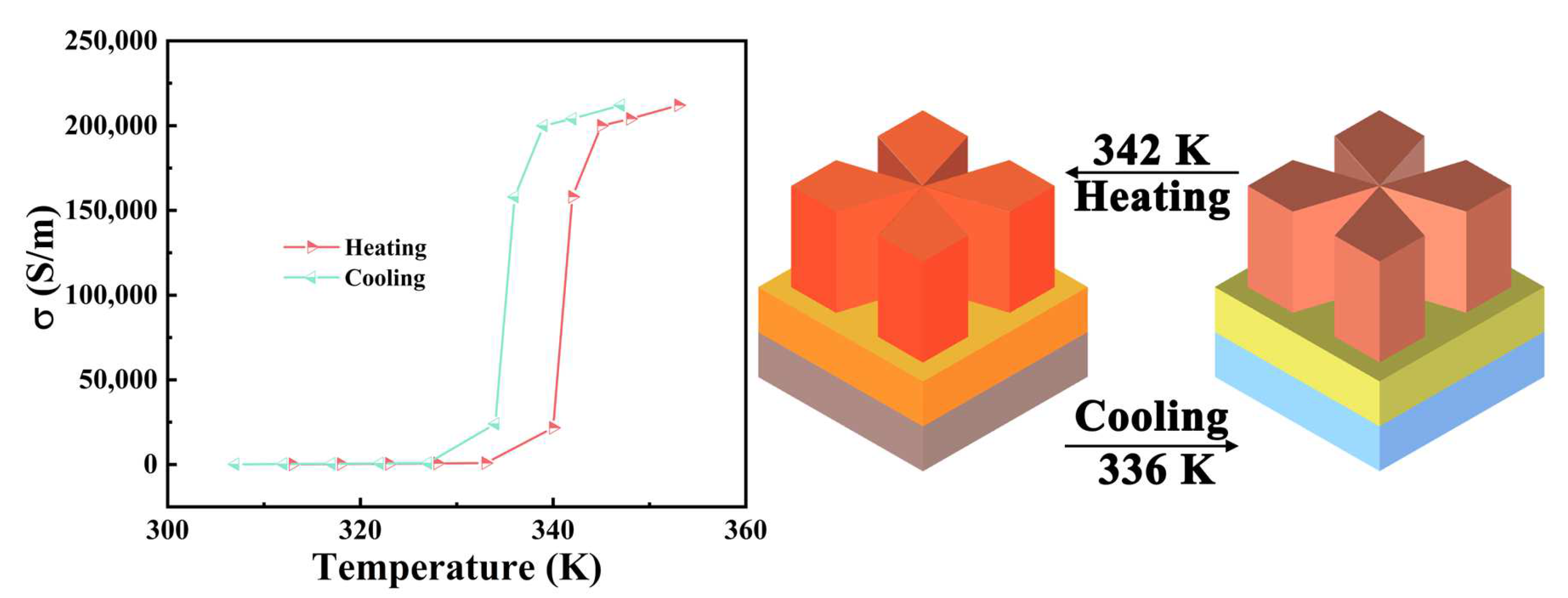
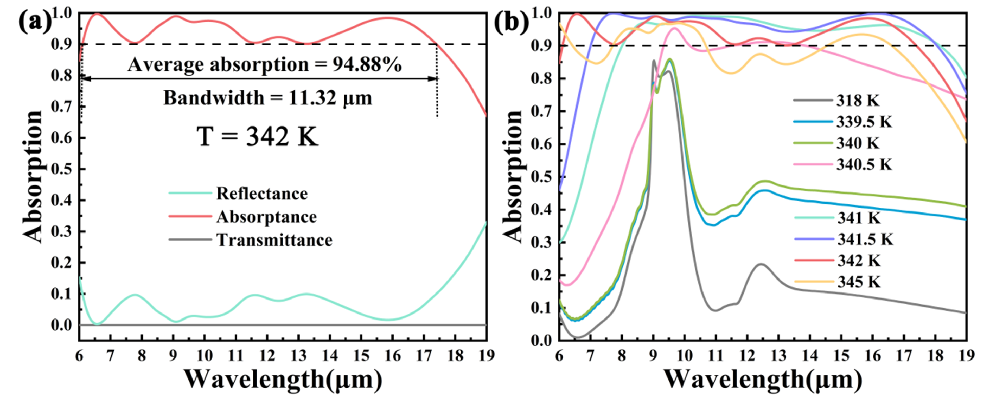
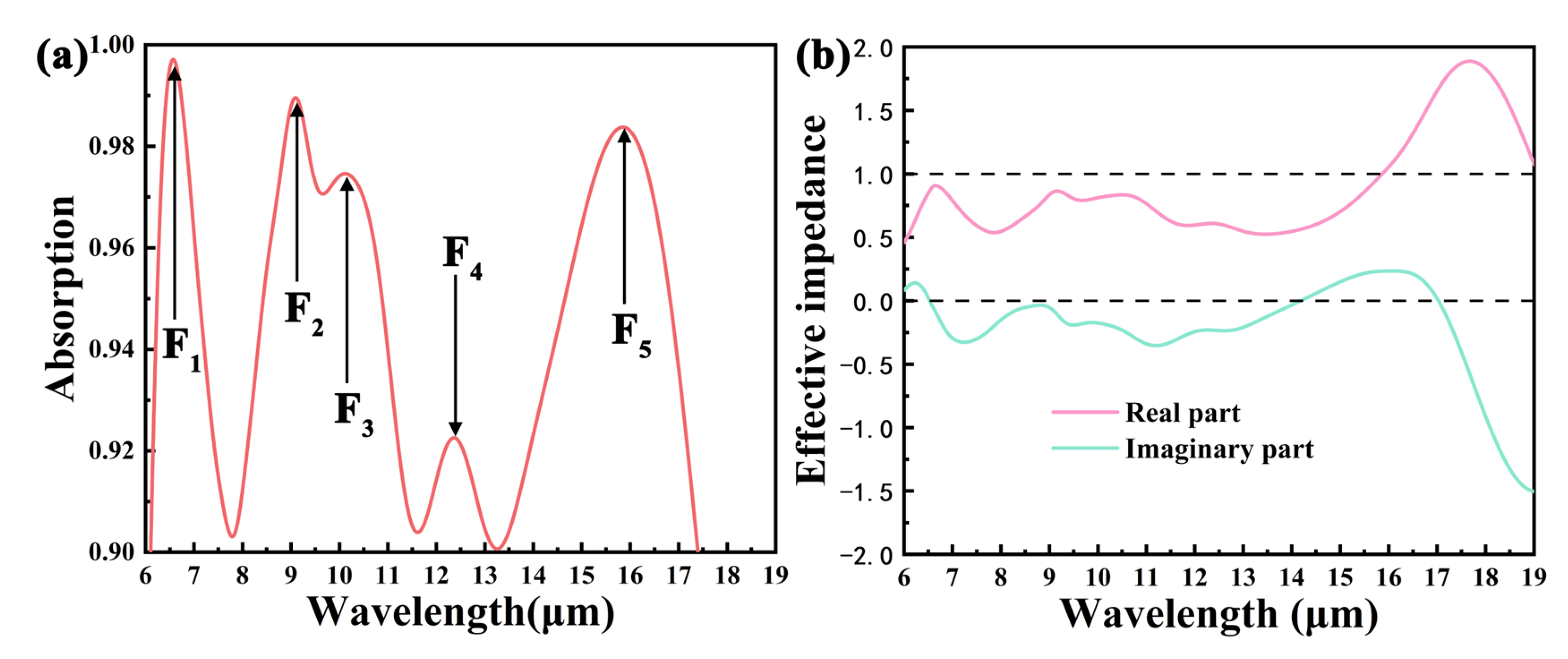
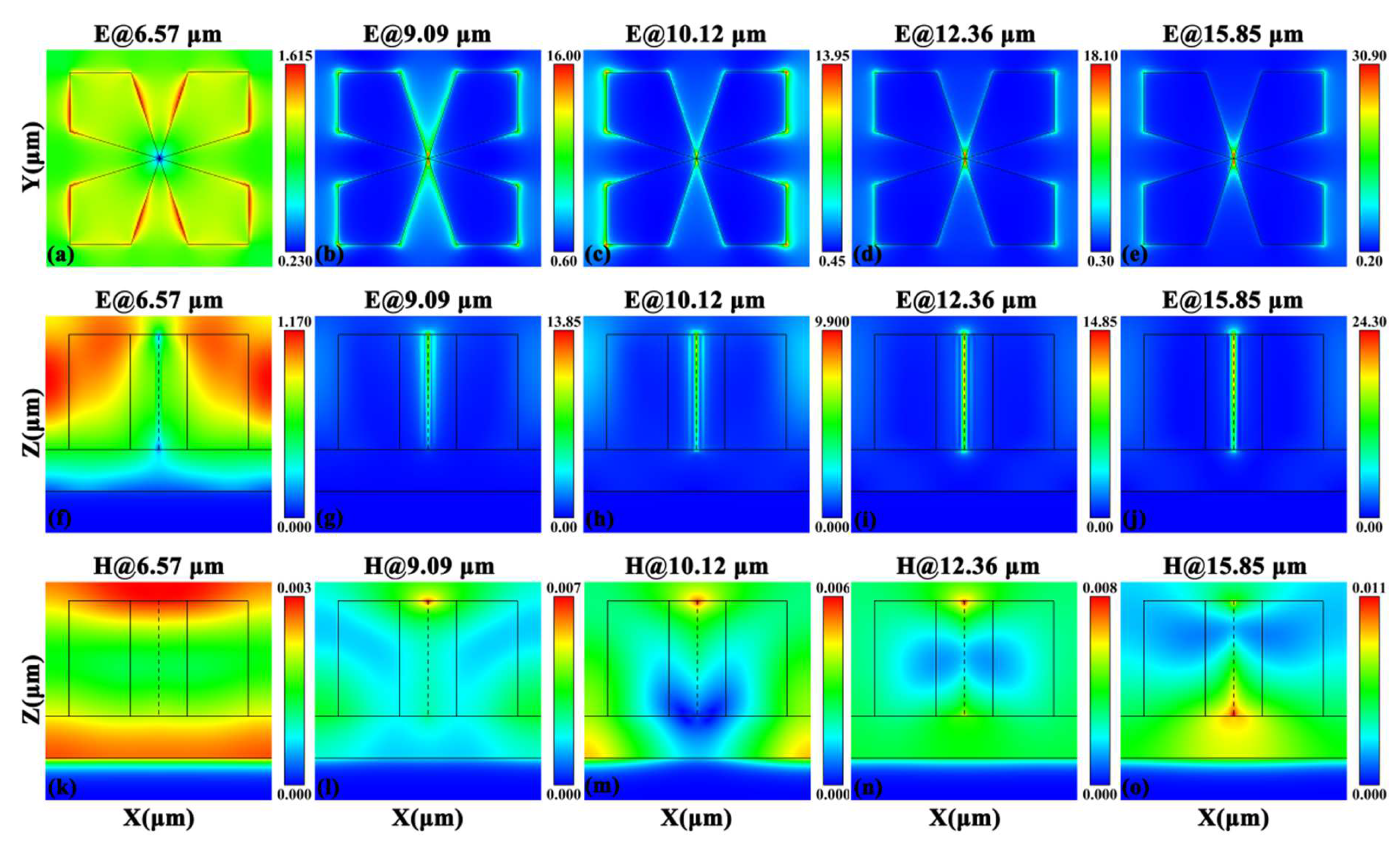
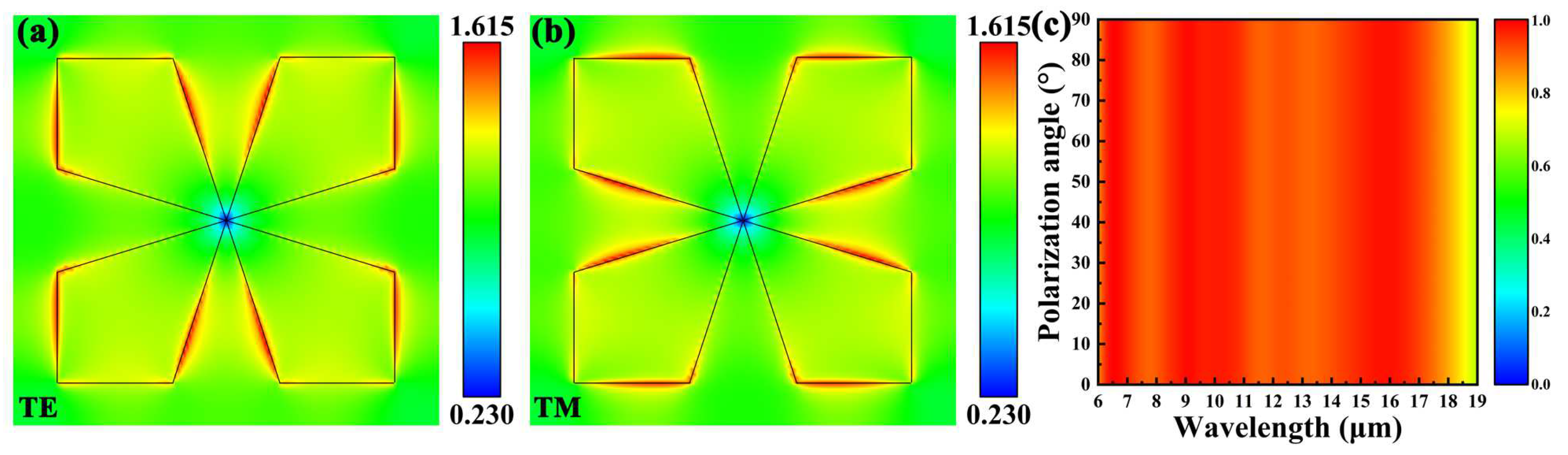
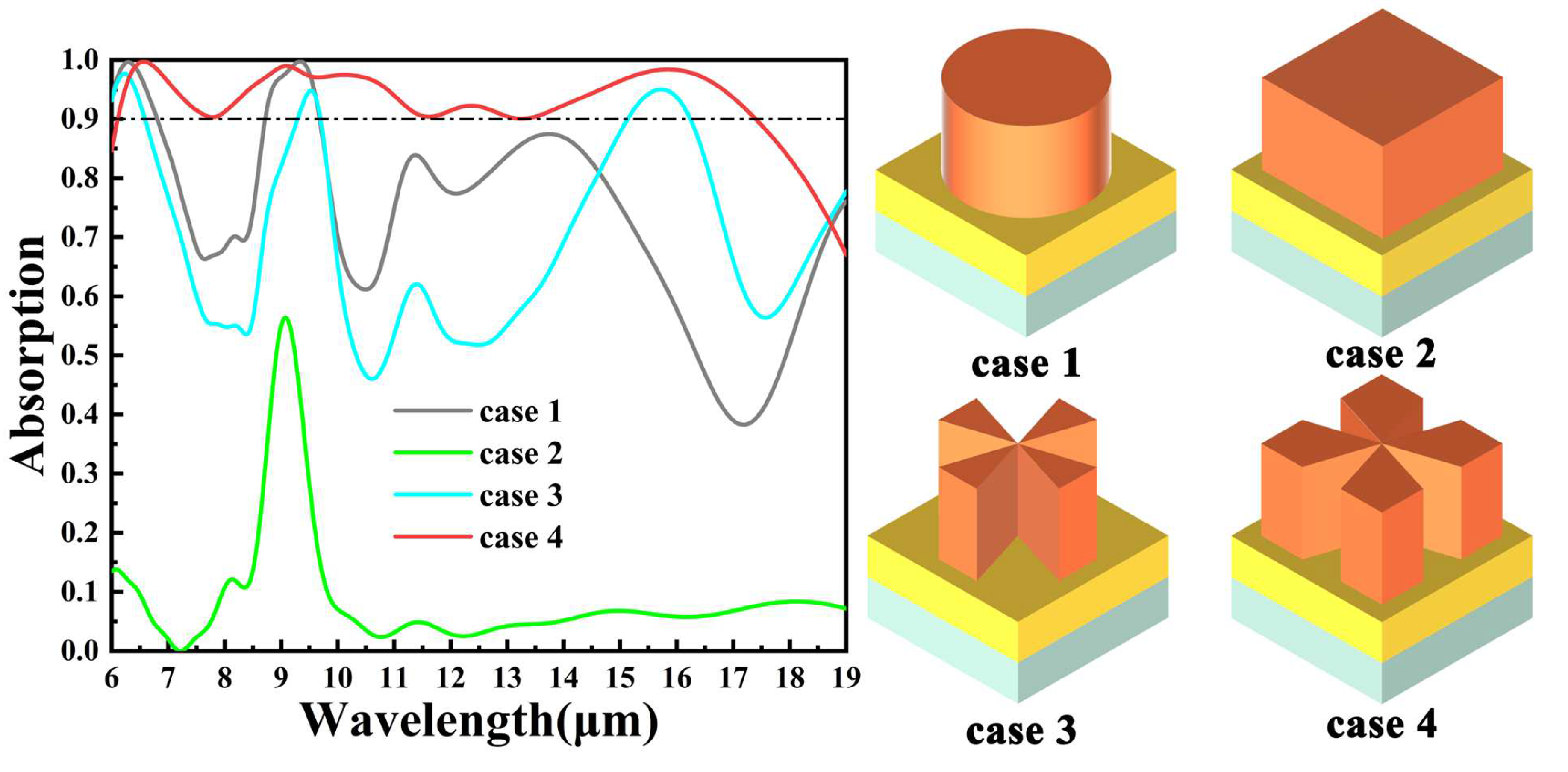
3. Calculation and Discussion

Figure 3a shows the absorption characteristic curve of the absorption device at 342 K temperature. After calculation, we found that its absorption bandwidth reaches 11.32 μm above 90%, and the average absorption in the working band (6.10–17.42 μm) is 94.88%. Figure 3b shows the absorption curves of the absorption device at different temperatures during warming. By calculating the absorption rate in the working band, we see that the absorption device has the lowest average absorption rate at 318 K, which is 20.61%. The average absorption at 339.5 K is 33.85%. It is 35.54% at 340 K, 62.62% at 340.5 K, 82.32% at 341 K, 92.08% at 341.5 K, and 89.99% at 345 K. The absorption device’s best absorption effect occurs at 342 K. The average absorption rate at this time is 94.88%. Our designed absorption device’s absorption rate can be therefore regulated by changing the temperature. The average absorption rate can be regulated between 20.61% and 94.88%. VO2 has a phase transition temperature of 340 K, which is critical for its thermochromic properties. For the optimum performance of an infrared absorber device, the operating temperature should be maintained within a range that allows VO2 to transition between insulating and metallic phases. Typically, this range is between 30 °C and 100 °C, depending on the specific design and application. Below 30 °C, VO2 remains in the insulating phase; above 100 °C, VO2 may degrade or lose the desired properties. Absorption devices also have requirements for the radiant power of the incident light. In the low power range (<10 mW/cm2), VO2 can operate normally, the phase change behavior is reversible, and the material does not degrade. In the medium power range (10–100 mW/cm2), the temperature of VO2 increases significantly with increasing incident light power. If the temperature exceeds the phase transition temperature but is below the degradation temperature, VO2 may temporarily lose its properties (e.g., dynamic optical properties), but this can be restored upon cooling. In the high power range (>100 mW/cm2), where the incident optical power is too high, the temperature of VO2 may exceed its degradation temperature, resulting in irreversible oxidation or structural damage of the material, which can lead to the loss of its properties. Taken together, the incident light power was controlled in the range of 10–50 mW/cm2 to avoid overheating and degradation [44,45].
It is well known that the peaks of the curves generally play an important role in the analysis. We have therefore investigated the absorption curve’s five absorption peaks in the working band in Figure 4a. By calculation, we obtained the corresponding wavelengths at these five absorption peaks. Among them, F1 = 6.57 μm, F2 = 9.09 μm, F3 = 10.12 μm, F4 = 12.36 μm, and F5 = 15.85 μm. The corresponding absorption values at these absorption peaks are 99.71%, 98.96%, 97.46%, 92.25%, and 98.38%, respectively. We calculate the effective impedance of the absorbing device by extracting the S-parameters of the absorbing device in our simulation. In Figure 4b, we give the effective impedance curve of the absorbing device. When the value of effective impedance is 1 + 0i, perfect absorption (100% absorption) can be realized [46]. Here, we bring the calculated effective impedance value into Equation (8) to calculate the peak absorption point. By comparison, it is found that the simulated absorption peak point remains consistent with the peak point calculated from the effective impedance. For broadband absorption in the absorption device, these absorption peaks play a decisive role. It is due to the superposition of multiple absorption peaks that more than 90% broadband absorption can be achieved.
In this section, we analyze the electromagnetic fields of the absorption device at the wavelengths corresponding to the absorption peaks to explain the broadband absorption mechanism of our designed absorption device. The electromagnetic field distributions at these five absorption peaks are shown in Figure 5a–o. In Figure 5a, it is observed that at F1, the electric field is primarily concentrated at the edge of the dart-shaped structure’s blade in VO2. Moving to Figure 5f, the electric field is predominantly focused in the upper section of the dart structure. The distribution of the magnetic field at F1 is illustrated in Figure 5k, where it is evident that the magnetic field is concentrated mainly at the upper end of the dart structure, the air on the surface, and the SiO2 dielectric layer. The reason for the electromagnetic field distribution at F1 is due to the fact that VO2 is in the metallic phase at this point. The frequency of the incident electromagnetic wave is equal to the collective oscillation frequency of free electrons, which excites the localized surface plasmon resonance (LSPR) of the VO2 layer [47]. When the incident electromagnetic wave reaches the interface between the metallic structure and the dielectric layer, the frequency of photons at this point matches the frequency of the propagating surface plasmon resonance [48,49]. Therefore, the propagating surface plasmon resonance (LSPR) is generated here. Moreover, an electric field exists in the dielectric layer at F1. This is due to the fact that electromagnetic waves are absorbed as they are reflected back and forth in the dielectric layer [50]. This is usually interpreted as the Fabry-Polo cavity resonance (FP-R). Therefore, the absorption peaks at F1 are mainly due to LSPR, PSPR, and FP-R. Figure 5b,g show the electric field distribution at F2. In the figure, it is evident that the electric field is concentrated at the central intersection of the dart-shaped VO2 layer, with the electric field also present along the edges of the dart. Furthermore, at this point, the electric field extends across the entire thickness of the VO2 layer. Moving to Figure 5l, it is evident that the magnetic field at F2 is primarily concentrated at the surface intersection of the dart-like VO2 layer. Taken together, the main reason for the generation of the absorption peak at F2 is the PSPR. Figure 5c,h show the electric field at F3. At this time, the electric field is concentrated at the intersection with the dart structure as well as at the tip. Moreover, the electric field is distributed throughout the thickness of the dart-like VO2 layer. As seen in Figure 5m, the magnetic field is concentrated at this wavelength at the intersection of the surface of the dart-like VO2 layer as well as at the interface between the ends of the SiO2 dielectric layer and the Ti substrate. It is analyzed that the absorption peaks at F3 are due to PSPR and LSPR [51]. Figure 5d,i show the electric field distribution at F4. As depicted in the figure, the electric field is concentrated at the intersection of the dart-like VO2 layer, extending through its entire thickness. Additionally, there is an electric field distribution along the edges of the dart. In Figure 5n, the magnetic field is primarily focused at the surface intersection of the dart-like VO2 layer, indicating that the absorption peak at F4 is mainly due to the plasmon-enhanced SPPR (Surface Plasmon Polariton Resonance) [52]. Figure 5e,j demonstrate the electric field distribution at F5, which resembles that at F2, yet with a slightly different magnetic field distribution. In Figure 5o, the magnetic field at F5 is concentrated at the lower intersection of the dart-shaped VO2 layer. By combining the electric field distribution, it can be inferred that the absorption peak at F5 is predominantly generated by the plasmon-enhanced SPPR. This section focuses on analyzing the mechanism underlying the absorption peaks of the absorption device. And these absorption peaks’ existence is the basis of broadband absorption that is generated by the absorption device.
In the preceding section, we explored the electromagnetic field distribution of the absorption device. Here, we delve into the impact of the shape parameters of the absorption device. Figure 6a illustrates the influence of the period length (P) of the unit structure of the absorption device on its absorption rate. The absorption peaks in the absorption curves experience a blueshift with an increase in period length, as depicted in the figure. For period lengths of P = 2.83 μm and 2.93 μm, the absorption device fails to achieve continuous absorption exceeding 90%. Conversely, at P = 3.13 μm and 3.23 μm, the absorption bandwidth of over 90% absorption narrows compared to that at P = 3.03 μm. Hence, we have selected P = 3.03 μm as the optimal cycle length for the unit structure of the absorption device. Figure 6b demonstrates the impact of the blade length (L) of the top dart-shaped VO2 layer of the absorption device on its absorption rate. Absorption rates above 90% continuous absorption were not attainable at L = 0.66 μm, L = 0.86 μm, and L = 0.96 μm. Additionally, the absorption bandwidth at L = 0.56 μm is narrower than that at L = 0.76 μm. Consequently, L = 0.76 μm has been identified as the optimal parameter. Figure 6c showcases the effect of the distance (W) between neighboring dart blades of the dart-shaped VO2 layer of the absorption device on its absorption. Notably, at W = 0.62 μm and 0.72 μm, the absorption bandwidth narrows compared to that at W = 0.82 μm. Furthermore, at W = 0.92 μm and 1.02 μm, the absorption rate mostly remains below 90%. Thus, W = 0.82 μm has been selected as the optimal parameter for the absorption device.
In the preceding section, we examined the shape parameters of the absorption device. In this section, we will delve into the thickness parameters of the absorption device. Figure 7a,b display the absorption spectra of the absorption device for varying thicknesses of the VO2 layer and SiO2 layer, respectively. From Figure 7a, it is observed that the absorption bandwidth of the absorption device exceeds 90% as the VO2 thickness (H1) increases from 1.18 μm to 1.38 μm. However, the absorption bandwidth narrows as H1 is further increased to 1.58 μm. Consequently, the optimal parameter for the VO2 thickness H1 is determined to be 1.38 μm. Figure 7b illustrates the impact of SiO2 thickness on the absorption rate. The absorption bandwidth of the absorption device exceeds 90% initially as the SiO2 thickness increases from H2 = 0.20 μm to H2 = 0.80 μm, reaching optimal absorption characteristics at 0.50 μm. Therefore, the optimal parameter for SiO2 thickness (H2) is chosen as 0.50 μm. Furthermore, upon comparing Figure 7a,b, it is noted that the absorption peaks of the absorption device undergo red-shifting as the thicknesses of both the VO2 and SiO2 layers increase. This red-shifting phenomenon is attributed to interference theory [53,54]. An increase in the thickness of the absorption device results in a greater phase difference in the electromagnetic wave, leading to a lengthening of the wavelength during resonance. In conclusion, the structural parameters of the absorption device have been optimized through an analysis of absorption rates at different structural parameters.
Table 2 demonstrates the comparison between previous studies and our design [55,56,57,58]. The comparison reveals that the absorption device of our design has a wider absorption bandwidth. Moreover, the absorption band of the absorption device covers the whole 8–14 μm. Our design also has a higher average absorptivity and the absorptivity is tunable. Not only that, but our design also has a simpler structure and is easier to fabricate compared to other designs. Therefore, our design has better absorption performance than previous designs.
The sensitivity to the angle of incidence and polarization plays a crucial role in the functionality of the device [59,60,61,62,63]. In contrast, the vector behavior of this infrared absorbing system of our design is characterized precisely by a polarization-insensitive response. This is attributed to the highly symmetric structure of the surface of the proposed infrared absorbing device. Due to the geometrical symmetry, light of different polarization directions excites similar electromagnetic resonance modes, and the electric field distribution and resonance modes are homogeneous, independent of the incident polarization direction. We show in Figure 8a,b the electric field distributions of the absorbing device in TE and TM modes for an electromagnetic wavelength of 6.57 µm. As shown, the surface electric field maps of the absorber device in TE and TM modes are rotationally symmetric and have the same intensity. This indicates that the electric field vectors exhibit the same pattern for TE polarization and TM polarization, which suggests that the electromagnetic response of the absorber device is consistent across polarization states. We scanned the polarization angle in 5° steps using FDTD simulation software. The scanning results are shown in Figure 8c. The results further confirm that the absorption spectra of randomly polarized light are almost identical, thus validating the polarization-independent nature of the system.
In this section, we explore the effect of the angle of incidence of electromagnetic waves on the absorbing device in different modes. Figure 9a shows the absorption spectra of the absorber device in TE mode for different incidence angles. It is observed that the absorption bandwidth remains relatively uniform in the range of 0–30° incidence angle. Subsequently, the absorption bandwidth shortens between 30° and 50° with very little change in absorption. As the angle of incidence exceeds 50°, especially between 50° and 60°, the absorption bandwidth and absorbance of the absorber decreases. Figure 9b,c show that the excitation position of the electric field on the surface of the absorber device does not change significantly as the angle of incidence increases, but the excitation intensity changes. Figure 9d illustrates the effect of different incidence angles on the absorber device for TM mode, which is similar to the trend observed in Figure 9a for TE mode. Figure 9e,f are also similar to the features in TE mode. Based on the above analyses, it can be concluded that the electromagnetic wave excites similar electromagnetic resonance (EMR) modes at varying angles of incidence, with only a slight change in intensity. Therefore, our designed absorber device is able to maintain excellent absorption characteristics even at larger incidence angles. This performance indicates the high potential applicability of our design [64,65,66].
In this study, we initially considered other surface shapes as well, such as circular or square structures. We exemplify several shapes in Figure 10 and give their absorption curves. As shown in the figure, the dart surface shape we designed consistently exhibits excellent performance in terms of absorption bandwidth and absorption efficiency. The sharp edges and corners of the surface structure of this dart shape enhance the local electromagnetic field strength, leading to stronger photomatter interactions [67,68]. This property is essential for achieving high absorption rates, as it maximizes the dissipation of energy within the metasurface structure. Moreover, this dart-like structure has a high degree of symmetry, making it inherently independent of polarization. This is a key feature for infrared absorption applications as it ensures consistent performance regardless of the polarization state of the incident light [69,70,71]. This property is particularly advantageous in practical applications where the polarization of the incident radiation may change.

4. Conclusions

In this study, an infrared metamaterial absorption device has been designed. Working at a temperature of 342 K, the absorption bands with over 90% absorption cover the range from 6.10 μm to 17.42 μm, with an absorption bandwidth of 11.32 μm that includes the mid-infrared atmospheric window (8–14 μm). The average absorption of the absorption device within this band reaches an impressive 94.88%. By changing the temperature to adjust the conductivity of VO2 within the device, the absorption rate of our designed device can be fine-tuned, allowing for an adjustable average absorption rate in the operating band ranging from 20.61% to 94.88%. The broadband absorption mechanism was explained by analyzing the electromagnetic field of the absorption device in the design. Structural parameters were optimized through parameter scanning techniques. Furthermore, a study on the sensitivity of the absorption device to both incident angle and polarization angle was conducted, showing the device’s strong insensitivity in these aspects. We strongly believe that our proposed design has great potential for future applications in energy harvesting, sensing, and electromagnetic stealth.

Author Contributions

Conceptualization, Z.H. and D.F.; data curation, Z.H., D.F. and Y.Y.; formal analysis, Z.H. and D.F.; methodology, Z.H., D.F. and Y.Y.; resources, Z.H., D.F. and Y.Y.; software, Y.Y.; data curation, Z.H., D.F. and Y.Y.; writing—original draft preparation, Z.H. and D.F.; writing—review and editing, Z.H., D.F. and Y.Y. All authors have read and agreed to the published version of the manuscript.

Funding

The authors are grateful for the support by the Major Special Projects in Yunnan Province (202302AF050001).

Institutional Review Board Statement

Not applicable.

Informed Consent Statement

Not applicable.

Data Availability Statement

Publicly available datasets were analyzed in this study. These data can be found at [https://www.lumerical.com/] (accessed on 1 January 2020).

Conflicts of Interest

The authors declare no conflicts of interest.

References

  1. Fei, Z. Electrically detecting infrared light. Nat. Mater. 2018, 17, 950–951. [Google Scholar] [CrossRef] [PubMed]
  2. Liu, J.J.; Yang, X.X.; Xu, Q.L.; Chang, R.G.; Wu, Z.H.; Shen, H.B. Unraveling the efficiency losses and improving methods in quantum dot-based infrared up-conversion photodetectors. Opto-Electron. Sci. 2024, 3, 230029. [Google Scholar] [CrossRef]
  3. Yan, C.C.; Che, Z.L.; Yang, W.Y.; Wang, X.D.; Liao, L.S. Deep-red and near-infrared organic lasers based on centrosymmetric molecules with excited-state intramolecular double proton transfer activity. Opto-Electron. Adv. 2023, 6, 230007. [Google Scholar] [CrossRef]
  4. Alecu, A.; Albu, C.; Badea, G.-I.; Alionte, A.; Enache, A.-A.; Radu, G.-L.; Litescu, S.-C. Infrared Laser-Assisted Extraction of Bioactive Compounds from Rosa canina L. Int. J. Mol. Sci. 2025, 26, 992. [Google Scholar] [CrossRef]
  5. Li, W.; Yi, Y.; Yang, H.; Cheng, S.; Yang, W.X.; Zhang, H.; Yi, Z.; Yi, Y.; Li, H. Active Tunable Terahertz Band-width Absorber Based on single layer Graphene. Commun. Theor. Phys. 2023, 75, 045503. [Google Scholar] [CrossRef]
  6. Argirusis, N.; Achilleos, A.; Alizadeh, N.; Argirusis, C.; Sourkouni, G. IR Sensors, Related Materials, and Applications. Sensors 2025, 25, 673. [Google Scholar] [CrossRef]
  7. Gu, Z.F.; Gao, Y.X.; Zhou, K.S.; Ge, J.; Xu, C.; Xu, L.; Rahmani, M.; Jiang, R.; Chen, Y.; Liu, Z.; et al. Surface-patterned chalcogenide glasses with high-aspect-ratio microstructures for long-wave infrared metalenses. Opto-Electron. Sci. 2024, 3, 240017. [Google Scholar] [CrossRef]
  8. Wang, H.Y.; Ma, R.; Liu, G.D.; Wang, L.L.; Lin, Q. Optical force conversion and conveyor belt effect with coupled graphene plasmon waveguide modes. Opt. Express 2023, 31, 32422. [Google Scholar] [CrossRef]
  9. Rane, S.; Prabhu, S.; Chowdhury, D.R. Physics and applications of terahertz metagratings. Opto-Electron. Sci. 2024, 3, 230049. [Google Scholar] [CrossRef]
  10. Luo, M.H.; Hu, J.Y.; Li, Y.M.; Bai, W.D.; Zhang, R.L.; Lin, Q.; Wang, L.L. Anapole-assisted ultra-narrow-band lattice resonance in slotted silicon nanodisk arrays. J. Phys. D Appl. Phys. 2023, 56, 375102. [Google Scholar] [CrossRef]
  11. Nurzed, B.; Saha, N.; Millward, J.M.; Niendorf, T. 3D Metamaterials Facilitate Human Cardiac MRI at 21.0 Tesla: A Proof-of-Concept Study. Sensors 2025, 25, 620. [Google Scholar] [CrossRef]
  12. Kang, D.H.; Heo, H.S.; Yang, Y.; Seong, J.; Kim, H.; Kim, J.; Rho, J. Liquid crystal-integrated metasurfaces for an active photonic platform. Opto-Electron. Adv. 2024, 7, 230216. [Google Scholar] [CrossRef]
  13. Li, Z.T.; Cheng, S.B.; Zhang, H.F.; Yang, W.X.; Yi, Z.; Yi, Y.G.; Wang, J.Q.; Ahmad, S.; Raza, R. Ultrathin broadband terahertz metamaterial based on single-layer nested patterned graphene. Phys. Lett. A 2025, 534, 130262. [Google Scholar] [CrossRef]
  14. Li, Y.M.; Tan, C.X.; Hu, J.Y.; Bai, W.D.; Zhang, R.L.; Lin, Q.; Zhang, Y.; Wang, L.L. Ultra-narrow band perfect absorbance induced by magnetic lattice resonances in dielectric dimer metamaterials. Results Phys. 2022, 39, 105730. [Google Scholar] [CrossRef]
  15. Berhe, A.M.; As’ham, K.; Al-Ani, I.; Hattori, H.T.; Miroshnichenko, A.E. Strong coupling and catenary field enhancement in the hybrid plasmonic metamaterial cavity and TMDC monolayers. Opto-Electron. Adv. 2024, 7, 230181. [Google Scholar] [CrossRef]
  16. Kowerdziej, R.; Ferraro, A.; Zografopoulos, D.C.; Caputo, R. Soft-Matter-Based Hybrid and Active Metamaterials. Adv. Opt. Mater. 2022, 10, 2200750. [Google Scholar] [CrossRef]
  17. Esfandiari, M.; Lalbakhsh, A.; Shehni, P.N.; Jarchi, S.; Ghaffari-Miab, M.; Mahtaj, H.N.; Reisenfeld, S.; Alibakhshikenari, M.; Koziel, S.; Szczepanski, S. Recent and emerging applications of Graphene-based metamaterials in electromagnetics. Mater. Des. 2022, 221, 110920. [Google Scholar] [CrossRef]
  18. Lee, Y. Metamaterials and Their Devices. Crystals 2025, 15, 119. [Google Scholar] [CrossRef]
  19. Fan, J.X.; Li, Z.L.; Xue, Z.Q.; Xing, H.Y.; Lu, D.; Xu, G.; Gu, J.; Han, J.; Cong, L. Hybrid bound states in the continuum in terahertz metasurfaces. Opto-Electron. Sci. 2023, 2, 230006. [Google Scholar] [CrossRef]
  20. Li, B.X.; Liu, M.L.; Wen, R.Q.; Wei, Y.; Zeng, L.L.; Deng, C.S. Dynamic control of Fano-like interference in the graphene periodic structure. J. Phys. D Appl. Phys. 2023, 56, 115104. [Google Scholar] [CrossRef]
  21. He, M.Y.; Wang, Q.Q.; Zhang, H.; Xiong, J.; Liu, X.P.; Wang, J.Q. Analog electromagnetic induced transparency of T-type Si-based metamaterial and its applications. Phys. Scr. 2024, 99, 035506. [Google Scholar] [CrossRef]
  22. Phan, T.N.K.; Kato, K.; Takano, K.; Fujioka, S.; Nakajima, M. Spectral Shape Control of Laser-Induced Terahertz Waves from Micro Split-Ring Resonators Made of Metallic Nanostructures. Photonics 2024, 11, 1209. [Google Scholar] [CrossRef]
  23. Wang, J.Q.; Sun, J.Y.; Sun, S.; Zhang, H.; Wang, Q.Q.; Yang, J.Y.; Mei, Y.W. Numerical simulation of electromagnetically induced transparency in composite metamaterial. Phys. Scr. 2025, 100, 025512. [Google Scholar] [CrossRef]
  24. Zeng, Z.L.; Liu, H.F.; Zhang, H.F.; Cheng, S.B.; Yi, Y.G.; Yi, Z.; Wang, J.Q.; Zhang, J.G. Tunable ultra-sensitive four-band terahertz sensors based on Dirac semimetals. Photonics Nanostruct.-Fundam. Appl. 2025, 63, 101347. [Google Scholar] [CrossRef]
  25. Xiao, Y.F.; Ma, C.; Sun, T.Y.; Song, Q.J.; Bian, L.; Yi, Z.; Hao, Z.Q.; Tang, C.J.; Wu, P.H.; Zeng, Q.D. Investigation of a high-performance solar absorber and thermal emitter based on Ti and InAs. J. Mater. Chem. A 2024, 12, 29145. [Google Scholar] [CrossRef]
  26. Ogawa, S.; Kimata, M. Metal-Insulator-Metal-Based Plasmonic Metamaterial Absorbers at Visible and Infrared Wavelengths: A Review. Materials 2018, 11, 458. [Google Scholar] [CrossRef]
  27. Avitzour, Y.; Urzhumov, Y.A.; Shvets, G. Wide-angle infrared absorber based on a negative-index plasmonic metamaterial. Phys. Rev. B 2009, 79, 045131. [Google Scholar] [CrossRef]
  28. Liang, S.; Cheng, S.; Zhang, H.; Yang, W.; Yi, Z.; Zeng, Q.; Tang, B.; Wu, P.; Ahmad, S.; Sun, T. Structural color tunable intelligent mid-infrared thermal control emitter. Ceram. Int. 2024, 50, 23611–23620. [Google Scholar] [CrossRef]
  29. Twaróg, R.; Szatkowski, P.; Pielichowska, K. Phase Change Materials in Electrothermal Conversion Systems: A Review. Energies 2025, 18, 569. [Google Scholar] [CrossRef]
  30. Li, W.; Cheng, S.; Zhang, H.; Yi, Z.; Tang, B.; Ma, C.; Wu, P.; Zeng, Q.; Raza, R. Multi-functional metasurface: Ul-tra-wideband/multi-band absorption switching by adjusting guided mode resonance and local surface plasmon resonance effects. Commun. Theor. Phys. 2024, 76, 065701. [Google Scholar] [CrossRef]
  31. Gao, H.; Fan, X.H.; Wang, Y.X.; Liu, Y.C.; Wang, X.G.; Xu, K.; Deng, L.; Zeng, C.; Li, T.; Xia, J.; et al. Multi-foci metalens for spectra and polarization ellipticity recognition and reconstruction. Opto-Electron. Sci. 2023, 2, 220026. [Google Scholar] [CrossRef]
  32. Zeng, L.L.; Li, B.X.; Wen, R.Q.; Zhang, X.J. Plasmonic Sensor Based on Multi Fano Resonance in Inverse T Shape Structure for Detection of CO2 Concentration. IEEE Photonics J. 2023, 15, 2201805. [Google Scholar] [CrossRef]
  33. Hu, J.Y.; Tan, C.X.; Bai, W.D.; Li, Y.M.; Lin, Q.; Wang, L.L. Dielectric nanocavity-coupled surface lattice resonances for high-efficiency plasmonic sensing. J. Phys. D Appl. Phys. 2022, 55, 075105. [Google Scholar] [CrossRef]
  34. Liu, Y.C.; Ma, X.M.; Chao, K.; Sun, F.; Chen, Z.; Shan, J.; Chen, H.; Zhao, G.; Chen, S. Simultaneously realizing thermal and electromagnetic cloaking by multi-physical null medium. Opto-Electron. Sci. 2024, 3, 230027. [Google Scholar] [CrossRef]
  35. Li, W.X.; Cheng, S.B.; Yi, Z.; Zhang, H.F.; Song, Q.J.; Hao, Z.Q.; Sun, T.Y.; Wu, P.H.; Zeng, Q.D.; Raza, R. Advanced optical reinforcement materials based on three-dimensional four-way weaving structure and metasurface technology. Appl. Phys. Lett. 2025, 126, 033503. [Google Scholar] [CrossRef]
  36. He, C.; Zhao, D.; Fan, F.; Zhou, H.; Li, X.; Li, Y.; Li, J.; Dong, F.; Miao, Y.-X.; Wang, Y.; et al. Pluggable multitask diffractive neural networks based on cascaded metasurfaces. Opto-Electron. Adv. 2024, 7, 230005. [Google Scholar] [CrossRef]
  37. Palik, E.D. Handbook of Optical Constants of Solids; Academic Press: Cambridge, MA, USA, 1998; Volume 3. [Google Scholar]
  38. Cheng, S.B.; Li, W.X.; Zhang, H.F.; Akhtar, M.N.; Yi, Z.; Zeng, Q.D.; Ma, C.; Sun, T.Y.; Wu, P.H.; Ahmad, S. High sensitivity five band tunable metamaterial absorption device based on block like Dirac semimetals. Opt. Commun. 2024, 569, 130816. [Google Scholar] [CrossRef]
  39. Liu, M.L.; Li, B.X.; Zeng, L.L.; Wei, Y.; Wen, R.Q.; Zhang, X.J.; Deng, C.S. Dynamic tunable narrow-band perfect absorber for fiber -optic communication band based on liquid crystal. J. Phys. D Appl. Phys. 2023, 56, 505102. [Google Scholar] [CrossRef]
  40. Yang, C.; Luo, M.H.; Ju, X.W.; Hu, J.Y. Ultra-narrow dual-band perfect absorber based on double-slotted silicon nanodisk arrays. J. Phys. D Appl. Phys. 2024, 57, 345104. [Google Scholar] [CrossRef]
  41. Mao, Y.; Zhang, H.; Xiong, J.; Liu, X.P.; Wang, Q.Q.; Wang, J.Q. Controlling of spontaneous emission of quantum dots based on hyperbolic metamaterials. J. Phys. D Appl. Phys. 2024, 57, 255111. [Google Scholar] [CrossRef]
  42. Nan, T.; Zhao, H.; Guo, J.; Wang, X.; Tian, H.; Zhang, Y. Generation of structured light beams with polarization variation along arbitrary spatial trajectories using tri-layer metasurfaces. Opto-Electron. Sci. 2024, 3, 230052. [Google Scholar] [CrossRef]
  43. Yu, Z.; Li, M.; Xing, Z.; Gao, H.; Liu, Z.; Pu, S.; Mao, H.; Cai, H.; Ma, Q.; Ren, W.; et al. Genetic algorithm assisted meta-atom design for high-performance metasurface optics. Opto-Electron. Sci. 2024, 3, 240016. [Google Scholar] [CrossRef]
  44. Yang, C.; Lin, Q.; Du, W.J.; Wang, L.L.; Liu, G.D. Bi-tunable absorber based on borophene and VO2 in the optical telecommunication band. J. Opt. Soc. Am. B 2022, 39, 2969–2974. [Google Scholar] [CrossRef]
  45. Xu, T.; Zhang, W.M.; Song, Q.J.; Yi, Z.; Ma, C.; Cheng, S.B.; Hao, Z.Q.; Sun, T.Y.; Wu, P.H.; Tang, C.J.; et al. Thermotunable mid-infrared metamaterial absorption material based on combined hollow cylindrical VO2 structure. Surf. Interfaces 2024, 52, 104868. [Google Scholar] [CrossRef]
  46. Li, B.X.; Zeng, L.L.; Wen, R.Q.; Zhang, X.J. Dynamic Regulation of Multiple Fano Resonances Based on Liquid Crystal. IEEE Photonics J. 2023, 15, 2200506. [Google Scholar] [CrossRef]
  47. Chen, Z.Y.; Cheng, S.B.; Zhang, H.F.; Yi, Z.; Tang, B.; Chen, J.; Zhang, J.G.; Tang, C.J. Ultra wideband absorption absorber based on Dirac semimetallic and graphene metamaterials. Phys. Lett. A 2024, 517, 129675. [Google Scholar] [CrossRef]
  48. Hu, J.Y.; Bai, W.D.; Tan, C.X.; Li, Y.M.; Lin, Q.; Wang, L.L. Highly electric field enhancement induced by anapole modes coupling in the hybrid dielectric-metal nanoantenna. Opt. Commun. 2022, 511, 127987. [Google Scholar] [CrossRef]
  49. Tan, Z.Q.; Lin, Q.; Du, W.J.; Wang, L.L.; Liu, G.D. Simultaneously enhance electric and magnetic Purcell factor by strong coupling between toroidal dipole quasi-BIC and electric dipole. J. Appl. Phys. 2025, 137, 033103. [Google Scholar] [CrossRef]
  50. Wan, M.; Li, C.; Bao, D.; Wang, J.; Lu, K.; Qu, Z.; Gao, H. Terahertz CMOS High-Sensitivity Sensor Based on Hybridized Spoof Surface Plasmon Resonator. Photonics 2025, 12, 102. [Google Scholar] [CrossRef]
  51. Jo, Y.; Park, H.; Yoon, H.; Kim, I. Advanced biological imaging techniques based on metasurfaces. Opto-Electron. Adv. 2024, 7, 240122. [Google Scholar] [CrossRef]
  52. Xiang, T.; Sun, Z.; Wang, L.L.; Lin, Q.; Liu, G.D. Polarization independent perfect absorption of borophene metamaterials operating in the communication band. Phys. Scr. 2024, 99, 085519. [Google Scholar] [CrossRef]
  53. Wang, X.Y.; Lin, Q.; Wang, L.L.; Liu, G.D. Dynamic control of polarization conversion based on borophene nanostructures in optical communication bands. Phys. Scr. 2024, 99, 085531. [Google Scholar] [CrossRef]
  54. Yang, J.P.; Tang, A.; Lian, B.W.; Xiong, Z.J.; Ma, Z.B.; Gu, N.T. Optimal multi-spectrum polarization detection with full-Stokes in a single channel by using standard retarders. Measurement 2025, 242, 116052. [Google Scholar] [CrossRef]
  55. Hou, E.; Meng, D.; Liang, Z.; Xiong, Y.; Yang, F.; Tang, Y.; Fan, Y.; Qin, Z.; Shi, X.; Zhang, Y.; et al. Mid-wave and long-wave infrared dual-band stacked metamaterial absorber for broadband with high refractive index sensitivity. Appl. Opt. 2020, 59, 2695–2700. [Google Scholar] [CrossRef]
  56. Qin, Z.; Meng, D.; Yang, F.; Shi, X.; Liang, Z.; Xu, H.; Smith, D.R.; Liu, Y. Broadband long-wave infrared metamaterial absorber based on single-sized cut-wire resonators. Opt. Express 2021, 29, 20275–20285. [Google Scholar] [CrossRef]
  57. Lian, Y.; Li, Y.; Lou, Y.; Liu, Z.; Jiang, C.; Hu, Z.; Wang, J. Adjustable Trifunctional Mid-Infrared Metamaterial Absorber Based on Phase Transition Material VO2. Nanomaterials 2023, 13, 1829. [Google Scholar] [CrossRef]
  58. Yang, F.; Liang, Z.; Shi, X.; Zhang, X.; Meng, D.; Dai, R.; Zhang, S.; Jia, Y.; Yan, N.; Li, S.; et al. Broadband long-wave infrared metamaterial absorbers based on germanium resonators. Results Phys. 2023, 51, 106660. [Google Scholar] [CrossRef]
  59. Li, Z.T.; Li, X.; Liu, G.D.; Wang, L.L.; Lin, Q. Analytical investigation of unidirectional reflectionless phenomenon near the exceptional points in graphene plasmonic system. Opt. Express 2023, 31, 30458. [Google Scholar] [CrossRef]
  60. Tang, C.J.; Nie, Q.M.; Cai, P.G.; Liu, F.X.; Gu, P.; Yan, Z.D.; Huang, Z.; Zhu, M.W. Ultra-broadband near-infrared absorption enhancement of monolayer graphene by multiple-resonator approach. Diam. Relat. Mater. 2024, 141, 110607. [Google Scholar] [CrossRef]
  61. Ma, R.; Zhang, L.G.; Zeng, Y.; Liu, G.D.; Wang, L.L.; Lin, Q. Extreme enhancement of optical force via the acoustic graphene plasmon mode. Opt. Express 2023, 31, 482723. [Google Scholar] [CrossRef]
  62. Medhat, M.; Malek, C.; Tlija, M.; Abukhadra, M.R.; Bellucci, S.; Elsayed, H.A.; Mehaney, A. One-Dimensional Photonic Crystals Comprising Two Different Types of Metamaterials for the Simple Detection of Fat Concentrations in Milk Samples. Nanomaterials 2024, 14, 1734. [Google Scholar] [CrossRef] [PubMed]
  63. Wang, Q.S.; Fang, Y.; Meng, Y.; Hao, H.; Li, X.; Pu, M.; Ma, X.; Luo, X. Vortex-field enhancement through high-threshold geometric metasurface. Opto-Electron. Adv. 2024, 7, 240112. [Google Scholar] [CrossRef]
  64. Chen, Y.; Zhang, S.M.; Tian, Y.; Li, C.; Huang, W.; Liu, Y.; Jin, Y.; Fang, B.; Hong, Z.; Jing, X. Focus control of wide-angle metalens based on digitally encoded metasurface. Opto-Electron. Adv. 2024, 7, 240095. [Google Scholar] [CrossRef]
  65. Yan, X.F.; Lin, Q.; Wang, L.L.; Liu, G.D. Tunable strong plasmon–exciton coupling based modulator employing borophene and deep subwavelength perovskite grating. J. Phys. D Appl. Phys. 2023, 56, 435106. [Google Scholar] [CrossRef]
  66. Huang, Z.; Liu, G.D.; Wang, L. Active modulation of quasi-bound state in the continuum based on bulk Dirac semimetals metamaterial. Appl. Phys. Express 2022, 15, 032006. [Google Scholar] [CrossRef]
  67. Hatsuoka, R.; Yamasaki, K.; Wada, K.; Matsuyama, T.; Okamoto, K. Tunable Plasmon Resonance in Silver Nanodisk-on-Mirror Structures and Scattering Enhancement by Annealing. Nanomaterials 2024, 14, 1559. [Google Scholar] [CrossRef]
  68. Zhang, Y.X.; Lin, Q.; Yan, X.Q.; Wang, L.L.; Liu, G.D. Flat-band Friedrich-Wintgen bound states in the continuum based on borophene metamaterials. Opt. Express 2024, 32, 10669–10678. [Google Scholar] [CrossRef]
  69. Xiao, Y.T.; Chen, L.W.; Pu, M.B.; Xu, M.F.; Zhang, Q.; Guo, Y.; Chen, T.; Luo, X. Improved spatiotemporal resolution of anti-scattering super-resolution label-free microscopy via synthetic wave 3D metalens imaging. Opto-Electron. Sci. 2023, 2, 230037. [Google Scholar] [CrossRef]
  70. Ling, Z.X.; Zeng, Y.; Liu, G.D.; Wang, L.L.; Lin, Q. Unified model for plasmon-induced transparency with direct and indirect coupling in borophene-integrated metamaterials. Opt. Express 2022, 30, 21966. [Google Scholar] [CrossRef]
  71. Zheludev, N.I.; Kivshar, Y.S. From metamaterials to metadevices. Nat. Mater. 2012, 11, 917–924. [Google Scholar] [CrossRef]
Figure 1. (a) Unit structure of the absorption unit. (b) A panoramic perspective of the unit structure of the absorption device. (c) Profile view unveiling the unit’s structure in the absorption device.
Photonics 12 00148 g001
Figure 2. VO2’s conductivity at different temperatures.
Photonics 12 00148 g002
Figure 3. (a) Absorption, reflectance, and transmittance curves of the absorbing device at 342 K. (b) Absorption curves of the absorption device at different temperatures.
Photonics 12 00148 g003
Figure 4. (a) Absorption peaks of 90% or more absorption curves. (b) Effective impedance of the absorption device.
Photonics 12 00148 g004
Figure 5. (ae) Electric field distribution in the XOY plane at the absorption peak of the absorption device. (fj) Electric field distribution in the XOZ plane at the absorption peak for the absorption device. (ko) Magnetic field distribution of the absorption device in the XOZ plane at the absorption peak.
Photonics 12 00148 g005
Figure 6. (a) Absorption spectra of the absorbing device at different cycle lengths. (b) Absorption spectra of the absorption device at different distances between neighboring darts. (c) Absorption spectra of the absorption device at different dart lengths.
Photonics 12 00148 g006
Figure 7. (a) Absorption spectra of the absorption device at different VO2 thicknesses. (b) Absorption spectra of the absorption device at different SiO2 thicknesses.
Photonics 12 00148 g007
Figure 8. (a) Surface electric field distribution of the absorbing device in TE mode at an incident wavelength of 6.57 µm. (b) Surface electric field distribution of the absorbing device in TM mode at an incident wavelength of 6.57 µm. (c) Absorption spectra of the absorption device at different polarization angles (0–90°).
Photonics 12 00148 g008
Figure 9. (a) Absorption spectra of the absorbing device in TE mode for different angles of incidence (0–60°). (b) Surface electric field distribution of the absorption device at θ = 0° incidence in TE mode. (c) Surface electric field distribution of the absorption device in TE mode at θ = 60° incidence. (d) Absorption spectra of the absorption device in TM mode at different angles of incidence (0–60°). (e) Surface electric field distribution of the absorption device in TM mode at θ = 0° incidence. (f) Surface electric field distribution of the absorption device in TM mode at θ = 60° incidence.
Photonics 12 00148 g009
Figure 10. Different surface shapes and corresponding absorption curves.
Photonics 12 00148 g010
Table 1. Structural parameters of the absorption device.
Parameter NamePLWH1H2H3
Parameter value (μm)3.030.760.821.380.500.50
Table 2. Comparison of our designed absorption device with previous designs.
ReferenceAbsorption BandAverage Absorption in the Operating BandShape of Structure UsedAdjustable Characteristics
[55]8.5–11.588%Stacked nanodisk structureNot possessed
[56]7.5–13.2591.7%Cross-Ti resonatorNot possessed
[57]6.5–11.595.7%Nanocylindrical arraysAdjustable absorption mode
[58]7.96–14.1696.5%NanocubeNot possessed
Our Design6.10–17.4294.88%Dart-shaped VO2 structureAverage absorption rate regulated within 20.61–94.88%
Disclaimer/Publisher’s Note: The statements, opinions and data contained in all publications are solely those of the individual author(s) and contributor(s) and not of MDPI and/or the editor(s). MDPI and/or the editor(s) disclaim responsibility for any injury to people or property resulting from any ideas, methods, instructions or products referred to in the content.

