Article

Simulated Microfluidic Device Constructed Using Terahertz Metamaterial for Sensing and Switching Applications

1
School of Physics and Electronic Engineering, Taishan University, Tai’an 271021, China
2
School of Physics and Information Engineering, Fuzhou University, Fuzhou 350108, China
*
Author to whom correspondence should be addressed.
Photonics 2025, 12(3), 194; https://doi.org/10.3390/photonics12030194
Submission received: 9 February 2025 / Revised: 23 February 2025 / Accepted: 24 February 2025 / Published: 25 February 2025

Abstract

:
We propose a microfluidic device that incorporates two layers of planar split-ring resonator (SRR)-based terahertz (THz) metamaterials and study its optical performance through simulation. The device features a concise design and leverages mature and straightforward fabrication processes. Our simulations reveal its remarkable sensing capabilities, with a sensitivity of up to 507.7 GHz/RIU for refractive index (RI) sensing and 16.03 GHz/μm for pressure sensing. Moreover, the device enables real-time monitoring, as it allows for a continuous flow of liquid between the layers. It can also function as an optical switch with a straightforward controlling method involving injecting and evacuating liquid. The maximum modulation depth (MD) achieved is 64.5%. The influence of fabrication errors during assembly of the two layers was studied in detail through simulation. The device demonstrates great robustness against fabrication imperfections, such as layer misalignment and spacer thickness variations, for most of the applications. Strict alignment is only necessary when targeting high-sensitivity RI sensing using the second resonance. The device’s unique combination of sensitivity, tunability, and compact design paves the way for potential applications in diverse fields, including biosensing, environmental monitoring, and optical communications.

1. Introduction

Terahertz (THz) metamaterials [1,2] have garnered significant attention in recent years for their unprecedented control over THz lightwaves and diverse applications in cloaking, superlenses, antenna technology, imaging, sensing, and many other fields [3,4,5,6,7]. They are composed of artificially designed periodic arrays of metallic resonators or dielectric structures, with their electromagnetic responses being meticulously engineered through precise modulation of geometric parameters. Among these structures, split-ring resonators (SRRs) stand out as a commonly used unit cell in constructing THz metamaterials. SRRs offer numerous advantages, including tunability, compactness, and strong resonant responses [8,9,10]. The fabrication technology for planar SRR-based metamaterials has matured since a decade ago. Through a series of micro-fabrication steps, including lithography, deposition of metal, and lift-off, such devices have been successfully prepared on silicon [11], quartz [12,13], and various flexible substrates [14,15].
In the context of sensing applications, THz metamaterials have demonstrated considerable promise. Linden et al. [16] have pointed out the similarity between SRRs and LC oscillator circuits, with the gap in the SRR functioning analogously to a capacitor. By placing testing samples at the gap, one can alter the permittivity of the gap area, resulting in a change in the resonant frequency. Based on this principle, earlier research typically involved statically applying the substance under test onto the surface of the planar device [11,17,18]. The substances detected included solutions of different concentrations [17], nanoparticles [11], and microorganisms [18], which were distinguished based on their various permittivities or, in other words, refractive indices (RIs). While these approaches provided a proof-of-concept for THz sensing, they often suffered from limited sensitivity, defined as the induced frequency shift Δf per unit change in the refractive index [19]. This limitation made it challenging to detect subtle changes in the samples. To address this issue, researchers have explored improved designs of SRR-based THz metamaterials that incorporate more complex structures [19,20,21,22] to enhance the sensitivity. In 2017, Wang et al. [19] revolutionized the traditional planar metamaterial structure by innovatively positioning the originally flat-lying SRR structure vertically on the device surface, thereby achieving a sensitivity of 332 GHz/RIU. Using the formula
| d λ d n | = C 0 f 0 2 d f d n
where C0 is the speed of the light in vacuum, f0 is the resonance frequency, λ is the wavelength, and n denotes the RI, they converted the sensitivity into 4.73 × 10⁴~1.04 × 10⁵ nm/RIU, demonstrating the superiority of THz sensing over optical sensing. This number even surpasses some of the recently reported work in optical sensing, with sensitivities up to only about 1000 nm/RIU [23,24,25]. Although inspiring, the fabrication process of such a device was too difficult, and the reported numbers were theoretical only. Following this, more efforts were devoted to revolutionizing the SRR structure. Park et al. fabricated SRRs with gap sizes as small as 200 nm [20], compared to a few micrometers in conventional designs. They were able to improve the sensitivity to 70 GHz/RIU. Meng’s group explored ways to etch a cavity right under the gap region [21] and sensed the photoresist S1813 (dielectric constant = 2.97) with a frequency shift of 86 GHz. This corresponds to a sensitivity of 49.9 GHz/RIU. In our previous work [22], we also fabricated SRRs on silicon substrates but etched the SRR pattern into the substrate to increase the height of the pattern while maintaining the thickness of the resonating metal layer. In this way, we detected polystyrene nanoparticles with a sensitivity up to 118 GHz/RIU. All these methods indicate the effectiveness of using SRRs for RI sensing, but also show the struggle and difficulty in achieving even higher sensitivity.
In addition to sensing applications, THz metamaterials have also been extensively investigated for amplitude modulation purposes. This unique feature paves the way for the realization of optical switches, enabling the controlled transmission/reflection level of THz lightwaves or blocking them at specific frequencies or frequency bands. Several studies have successfully demonstrated the ability to manipulate the amplitude of the THz spectrum using metamaterial-based devices [26,27]. However, traditional methods of achieving such amplitude modulation often involve altering the device structure through changes in the component layout [28,29] or material composition [30,31]. To change the structural layout, control methods such as electrical biasing [28,29] are usually cumbersome. Pumping [30,32] and heating [31,33] are also commonly used control methods, but they require the incorporation of expensive photosensitive or thermos-sensitive materials into the device, thereby increasing the complexity and cost of fabrication.
In this study, we propose a microfluidic device that incorporates planar SRR-based THz metamaterials as its core components. This device possesses the ability to dynamically monitor liquids as they continuously pass through it, detecting subtle changes within the liquid, such as concentration variations or the presence of pollutants. Its optical performance is studied through simulation. The sensitivity of the device achieves an impressive level of 507.7 GHz/RIU. It can also work as a pressure sensor, with a sensitivity of up to 16.03 GHz/μm. Furthermore, the device can function as an optical switch with a straightforward control method. By simply injecting or draining an isopropyl alcohol (IPA) solution or water, the transmission of incoming THz lightwaves can be efficiently switched “on” and “off”. The simulation results reveal that the maximum modulation depth (MD) reaches 64.5%. These features enable the design to be a promising candidate in areas including biomedicine, environmental monitoring, and advanced materials research.

2. Materials and Methods

2.1. Device Design and Definition of Parameters

Figure 1a depicts the design of the proposed microfluidic device. It is composed of two identical layers, each of which is a planar THz metamaterial with an aluminum SRR array on a quartz substrate. The thicknesses of the metal pattern and the substrate are 0.2 and 50 μm, respectively. The SRRs on the top and bottom layers of the device are arranged to face oppositely in the y-direction. Figure 1b shows a unit cell of such a device. The spacing between the top and bottom quartz substrates is denoted as h. To study its impact on the device performance, it was varied from 2 to 10 μm in this study. Figure 1c illustrates the top view of the unit cell, highlighting the SRRs. The length of the SRRs (l) is 60 μm. The width (d) is 32.5 μm. The gap (g) and line width (w) are both 5 μm. The length of the metal bar in the gap region (m) is 12.5 μm. These dimensions make sure that the SRR resonates with the THz lightwave in the frequency range of interest, which is 0.1~2 THz. The unit cell is repeated in the x- and y-directions, with a lattice constant (P) of 80 μm in both directions. For the ease of description, the gap bearing side will be referred as the “G-edge”, and its opposite edge as the “O-edge” hereinafter. The two SRRs in the unit cell are not required to be in a fixed relative position. To study the impact of misalignment between the layers, the SRRs on the top and bottom layers are spaced in the y-direction with a distance Δy between the O-edges. In the following study, Δy ranges from −5 to 20 μm. When Δy = −5 μm, the O-edges of both SRRs overlap when viewed from the top; when Δy = 20 μm, the G-edge of the top SRR overlaps with that of the bottom SRR in the adjacent unit cell in the top view. On the other hand, the offset of the two SRRs in the x-direction is denoted as Δx. We studied the impact of Δx in the range of 0 to 20 μm. When Δx = 20 μm, the span of the two SRRs in the x-direction reaches a lattice constant of 80 μm.

2.2. Simulation Method

To numerically investigate the optical properties of the device, the software “3D FDTD Solutions” (three-dimensional finite-difference time-domain solutions) was used to calculate the transmission spectra of the structure and the electromagnetic (EM) field distribution within it. To achieve this, a single-unit structure was created within the software, utilizing periodic boundary conditions within the x-y plane and employing perfectly matched layer (PML) boundaries along the z-direction. THz plane wave that is polarized in the y-direction strikes the device perpendicularly and propagates along the z-direction through the device. A typical device was first studied as the baseline with a set of parameters: h = 8 μm, Δx = 0, and Δy = 15 μm. These parameters were then varied according to the given range. To simulate the various liquids passing through the device, a background index ranging from 0 (air) to 2.1 (typical value for water) was set during the simulation. In the software, a monitor for data collection was set at the bottom of the device to record the transmission spectra, while another was set at the interface between the metal pattern and the substrate of the lower layer for observation of the EM distribution maps. As the device is symmetrical top to bottom, the recorded EM distribution maps are applicable for both layers.

2.3. Illustration of Possible Fabrication Method and Experimental Setup

Although this study mainly focuses on simulation results, such a device can easily be realized. The core components of the structure are the top and bottom layers, which are conventional THz metamaterials composed of metal patterns fabricated on a quartz substrate. Each layer can be fabricated using a standard micro-fabrication method, involving lithography, metal deposition, and lift-off steps. Such devices have been successfully fabricated and characterized for a decade [12,13]. The fabrication process has been developed ever since. To assemble the two layers together, bonding epoxy can be used. This also acts effectively as the spacer between the layers, with its thickness defining the interlayer distance h. To be more specific, SU-8 can be used as the bonding material. It can be spin-coated onto the surface of the bottom layer, and the thickness is controlled by the spin-coating speed. The SRR pattern should be protected during this step. Covering the protected area by tape is a feasible solution [13]. After peeling off the tape and revealing the SRR pattern, the bonding area has thus been defined. By pressing the top layer into hard contact with SU-8 and curing it using ultraviolet light, the bonding epoxy is solidified. Inlet and outlet holes can be punched in the top substrate, and thereby, liquids can be introduced through tubes into the microfluidic chamber that is formed between the layers. With the THz lightwave being projected perpendicularly onto the device surface, detectors can detect the transmitted light on the other side of the device. Transmission spectra are obtained in this way. Figure 1d illustrates such a device and the experimental setup.
The biggest challenge during fabrication will be the precise control of the spacer thickness and the alignment of the top and bottom layer. For this very reason, h, Δx, and Δy are kept variable, and their impact on the resonances are studied independently through simulation.

3. Results and Discussions

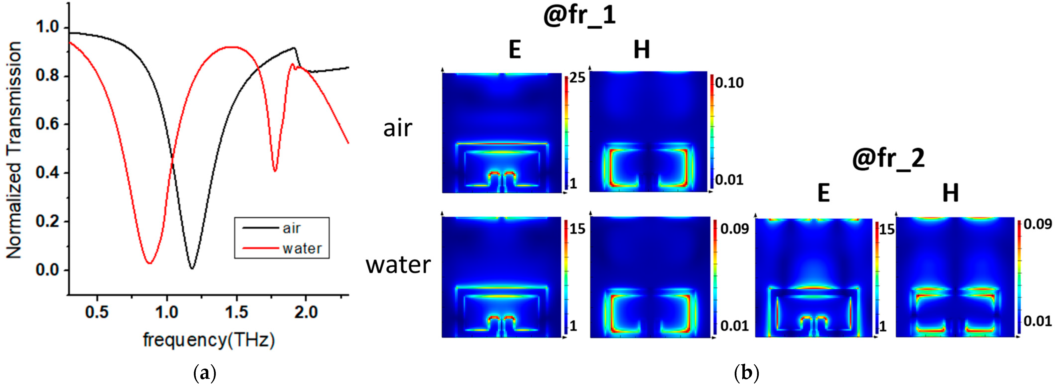
3.1. The Baseline Performance of a Typical Device

Figure 2a displays the simulated transmission spectra of a typical device with air (n = 1) and water (n = 2.1) as the interlayer media. Within the frequency range of 0.3 to 2.3 THz, the device exhibits a resonant dip at 1.178 THz when filled with air. When water fills the interlayer, this resonance shifts to 0.873 THz (a red shift), and an additional resonance appears at 1.775 THz. The EM distribution maps at these resonant frequencies are shown in Figure 2b.
At the first resonance, the H-fields within the device reveal oscillating currents along the left and right sides of the SRR at the bottom layer. Note that the same currents are also symmetrically present at the top layer. This results in charges accumulating at the outer rim of the O-edge (see the E-field distribution), forming capacitance between the O-edges of both the top and bottom SRRs. According to the LC model of the SRR [16],
ω r = 1 L C
the resonant frequency ωr is determined by the effective inductance (L) and capacitance (C) of the system. Changing from air to water as the interlayer media leads to an increase in permittivity; therefore, C increases, resulting in a lower resonant frequency.
During these resonant conditions, the oscillating currents and accumulated charges at the O-edges of the SRRs create a strong electromagnetic field interaction with the surrounding medium. This interaction leads to the collective oscillation of free electrons within the metallic SRRs, known as plasmons. Specifically, at the resonant frequencies, the electromagnetic field enhances the coupling between the incident terahertz wave and the free electrons in the SRRs, exciting the plasmon modes. The localized charge distributions and electric field enhancements at the O-edges further facilitate the plasmon excitation, as they provide hotspots for electron–electromagnetic wave interactions.
When the device is filled with water at the second resonance, according to the H-field distribution in the device presented in Figure 2b, the surface currents break into four sections, along the left and right halves of the G-edge and O-edge, respectively. The current path is shorter than that at the first resonance, and consequently, the charges oscillate at a higher frequency. On the other hand, although coupling between the top and bottom layers is still present (see the E-field distribution), it is mostly concentrated at the center of the O-edge, in contrast with the uniform distribution along the O-edge at the first resonance. By analogy to the parallel plate capacitor, whose capacitance is proportional to the plate area, such charge concentration means a reduction in the capacitor area and, hence, a reduction in capacitance. This also leads to an increased resonant frequency.
At the second resonance, the altered current distribution and charge concentration result in a different plasmon excitation scenario. The shorter current path and concentrated charge distribution at the O-edge create a more confined electromagnetic field, which enhances the interaction with free electrons in a localized region. This confinement leads to the excitation of higher-frequency plasmon modes, contributing to the emergence of the additional resonance peak at 1.775 THz.
To investigate the spectral variations as a function of the liquid refractive index (RI), we varied the RI of the filling substance from n = 1.0 to n = 2.1 in increments of 0.1. The resulting transmission spectra are depicted in Figure 3a. The color bar represents the normalized transmission amplitude. The corresponding line curves are shown in Figure 3c,d. A linear shift is evident in both the lower resonant frequency range (when n varies from 1.0 to 2.1) and the higher resonant frequency range (when n varies from approximately 1.8 to 2.1). Figure 3b illustrates the relationship between the resonant frequencies and the RI. The linear fitting results indicate R-squared values close to one for both resonant modes, suggesting a strong linear correlation between the resonant frequencies and the RI of the filling substance. The sensitivity of the device was found to be 282 GHz/RIU and 433 GHz/RIU for the two resonant modes, respectively. These numbers can be converted to 6.1 × 10⁴~1.1 × 10⁵ nm/RIU and 3.6 × 10⁴~4.1 × 10⁴ nm/RIU, according to Equation (1). They represent a significant improvement compared to recently reported RI sensors (see Table 1).
Figure 3d shows the transmission dips at the second resonance. The resonance is only prominent for n = 1.8 and above. The appearance of the second resonant dip demonstrates amplitude modulation at the resonant frequency, which is the underlying principle for optical switching. The MD is defined as follows:
MD = (Amax − Amin)/Amax × 100%,
where Amax and Amin refer to the maximum and minimum transmission amplitude at the resonant frequency. In Figure 3d, the resonant intensity peaks at n = 1.9, suggesting optimal amplitude modulation when using this liquid as the medium. Reference [45] confirms that IPA has an RI of 1.9. Hence, the proposed device can effectively function as an optical switch simply through the injection or evacuation of this inexpensive and readily accessible liquid. In our typical device, IPA yields an MD of 60.7%. Alternatively, water can be used, achieving an MD of 56.3%. These numbers also indicate a notable enhancement when compared to THz metamaterial modulators that have been recently reported (see Table 2).
Next, the impacts of the dimension parameters h, Δx, and Δy on sensing and switching applications are investigated separately. These results will provide insights into the allowable error tolerance during fabrication, as well as guide the optimization of the structural design.

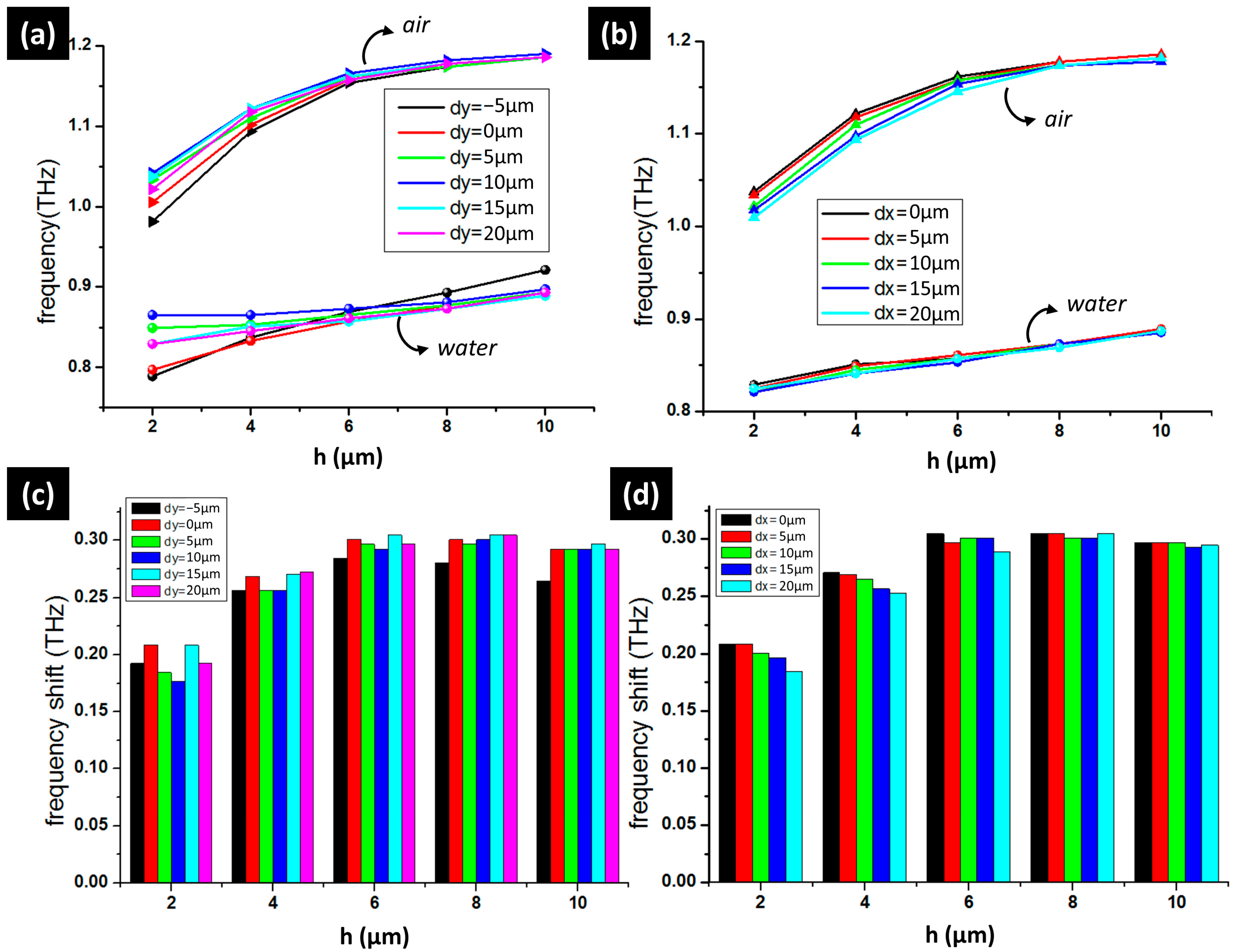
3.2. Impacts of h, Δx, and Δy on Sensing with the First Resonance

3.2.1. RI Sensing

The impact of the parameters on the first resonance is summarized in Figure 4. The effects of Δx and Δy are studied independently. For data shown in Figure 4a, Δx is fixed at 0, while Δy varies from −5 to 20 μm. In Figure 4b, Δy is fixed at 15 μm, while Δx varies from 0 to 20 μm. In Figure 4a,b, it is evident that the resonant frequencies increase with the substrate distance h. This can be understood through the analogy between the coupling O-edges and a parallel plate capacitor. The formula for the capacitance of a parallel plate capacitor is given by
C = εA/d,
where ε is the permittivity of the dielectric between the metal plates, A is the area of the two parallel metal plates, and d is the distance between the plates. When the substrate distance h increases, d is effectively enlarged. Consequently, the capacitance decreases, leading to an increase in the resonant frequency.
From Figure 4a, we can see that the effect of Δy becomes less prominent as h increases, supported by the fact that the resonant frequencies generally converge. This suggests that the vertical distance between the O-edges becomes a dominant factor over their horizontal spacing in determining the interlayer capacitance. The only exception is when Δy = −5 μm and the device is filled with water. This is when the coupling O-edges overlap in the top view. On the other hand, Figure 4b shows that the resonant frequencies have less dependency on Δx. Figure 4c,d present the frequency shift (Δf), calculated from data in Figure 4a,b. As a result, we can see that the variation between Δf when h is small (2 and 4 μm) is more distinctive than when h is fairly large (6~10 μm). A large Δf of about 300 GHz is achieved for all cases when h is larger than 4 μm, except for the device where Δy = −5 μm, which is the only exception, as previously discussed. This means that when h is greater than 4 μm, the displacement between the top and bottom SRRs becomes insignificant if Δf, or sensitivity, is the major concern. These results suggest that if the first resonance is used for RI sensing, the fabrication process can be simplified. As long as the substrates are separated by ≥6 μm and the metal patterns do not overlap when viewed from above, the frequency shift stabilizes at an average of 298 GHz with a standard deviation (SD) of 0.004 GHz. To sum up, if the first resonance of the device is intended for RI sensing, there is great fabrication tolerance in terms of the substrate distance and alignment of the top and bottom layers.

3.2.2. Pressure Sensing

In Figure 4a,b, a linear relationship between the resonant frequency and the substrate distance is also observed when the device is filled with water. Here, we consider the change in interlayer spacing to be deformation caused by pressure. The resulting change in resonant frequency indicates that the device can spectrally reflect the magnitude of deformation, making it suitable for use as a pressure sensor. The best sensitivity can reach 16.03 GHz/μm for the device with Δy = −5 μm and Δx = 0, illustrated by the black curve in Figure 4a. For the curves in Figure 4b, the sensitivity stabilized at about 8.1 GHz/μm, suggesting that misalignment of the top and bottom layers in the x-direction has minimal influence on the sensitivity.

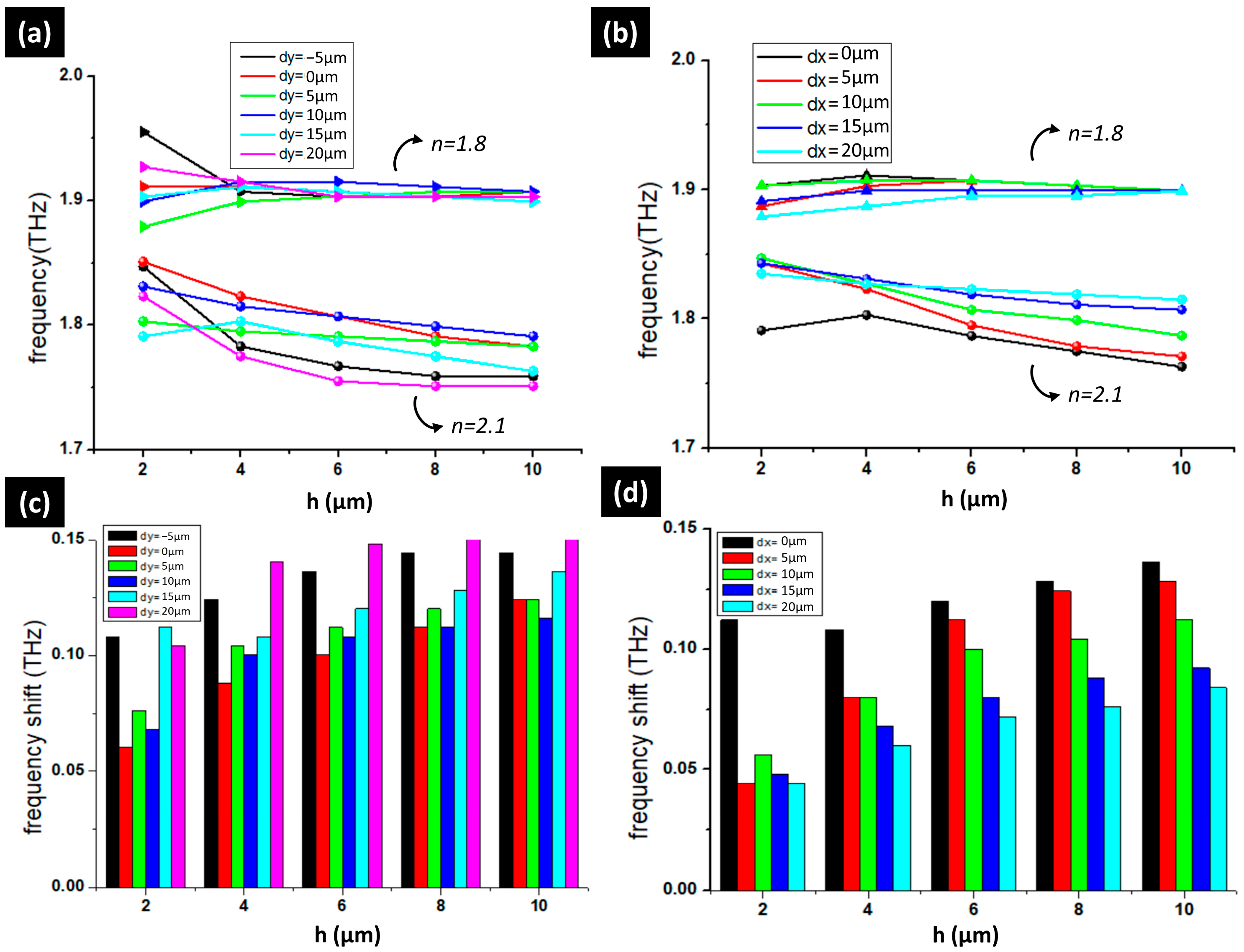
3.3. Impacts of h, Δx, and Δy on Sensing with the Second Resonance

The impact of the dimension parameters on the second resonance is summarized in Figure 5. Similarly, the effects of Δx and Δy are studied independently. For data shown in Figure 5a, Δx is fixed at 0, while Δy varies from −5 to 20 μm. In Figure 5b, Δy is fixed at 15 μm, while Δx varies from 0 to 20 μm. In both Figure 5a,b, we can see that for a filling substance with n = 1.8, the second resonant frequency converges as h increases, meaning that the effect of misalignment in the x- and y-directions diminishes as the distance between the two layers increases. But for devices filled with water (n = 2.1), this is not the case.
In Figure 5a, the resonant frequencies gradually decrease but also gather into two groups when h reaches 10 μm. The first group includes Δy = 0, 5, and 10 μm, and the second group includes Δy = −5, 15, and 20 μm. Taking into consideration that Δy = −5 and 20 μm means that there is an overlap between the two layers from the top view, the difference between these two groups lies in how dispersed the SRRs are in the top view. When the G-edges or O-edges overlap, from a capacitance point of view, the distance between the coupling edges is reduced, leading to an increased capacitance and therefore a reduced resonant frequency.
The fact that Δy = 0 and 15 μm go into different groups can be attributed to a similar reason. Δy = 0 represents the case where the G-edge of the top SRR is on the verge of overlapping with that at the bottom, whereas Δy = 15 μm means that the O-edges are on the verge of overlapping. The capacitance is understandably larger for the Δy = 15 μm case, as the coupling edges are longer due to the missing gap. The same trend can be observed in the resonant frequencies for a filling substance with n = 2.1 in Figure 5b. The frequencies gradually decrease but sort themselves according to Δx as h reaches 10 μm. The bigger Δx is, the shorter portions of the top and bottom edges can couple to each other, and thus, the higher the resonant frequency is located.
Figure 5c,d demonstrate the resulting frequency shift (Δf) when the filling substance changes from n = 1.8 to n = 2.1. As the resonant frequencies for n = 1.8 changes little as h increases, and as for n = 2.1, they decreases with h, an increasing trend of Δf with h is firstly observed for almost all sets of data, especially when h is greater than 2 μm. Secondly, for the reasons explained above, Δf is especially high when the top and bottom SRRs have edges overlapping in the top view (Figure 5c) and becomes smaller as the SRRs become more and more misaligned in the x-direction (Figure 5d). To sum up, if the second resonance is intended for a sensing substance with n from 1.8 to 2.1, strict alignment of the SRRs in the x-direction is preferred, and the top and bottom SRRs should have overlapping edges in the top view. Moreover, a substrate distance larger than 6 μm is preferred for a higher sensitivity. The largest sensitivity can reach 507.7 GHz/RIU when Δy = 20 μm, Δx = 0, and the substrate distance is 8 or 10 μm.

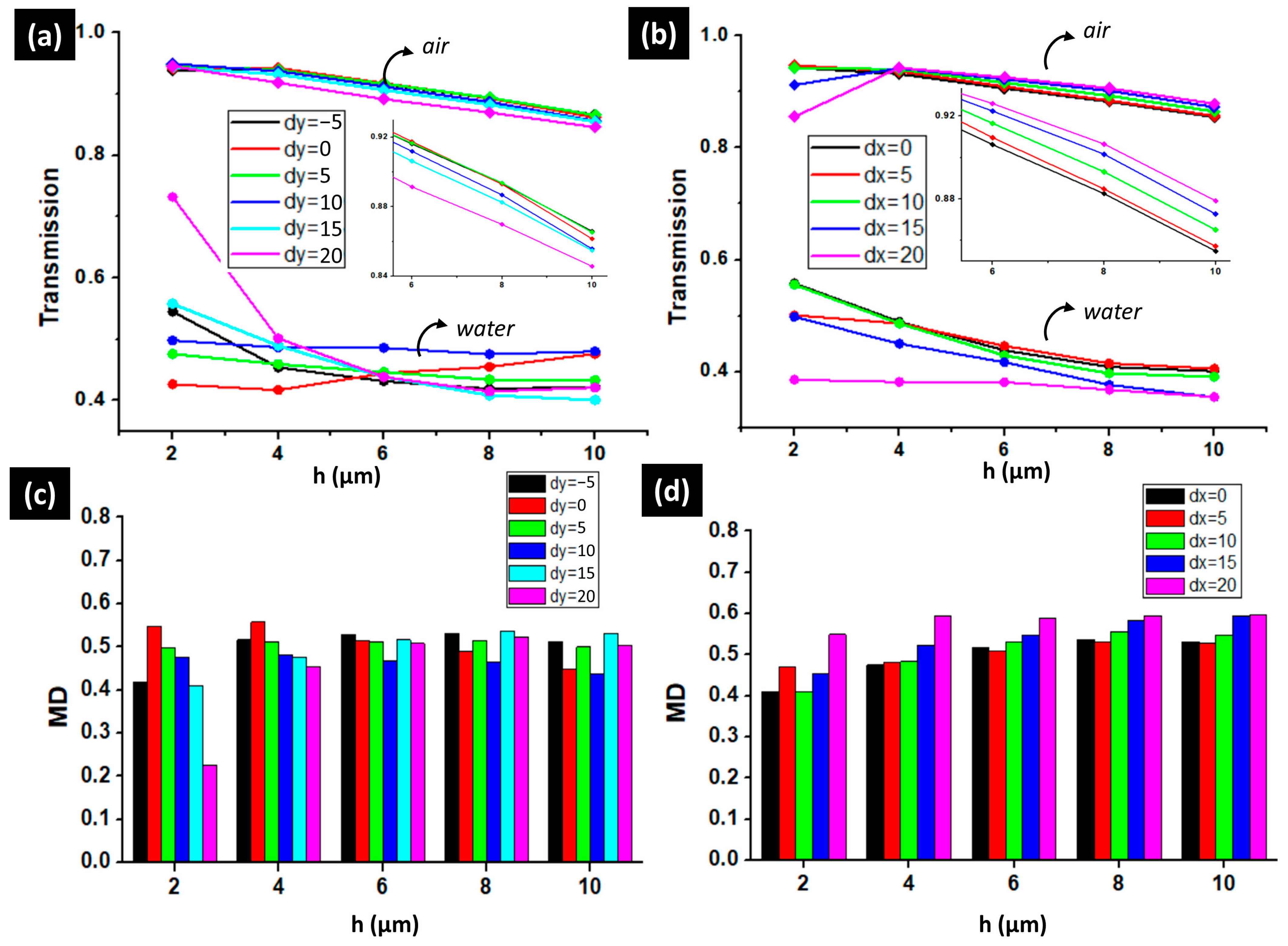
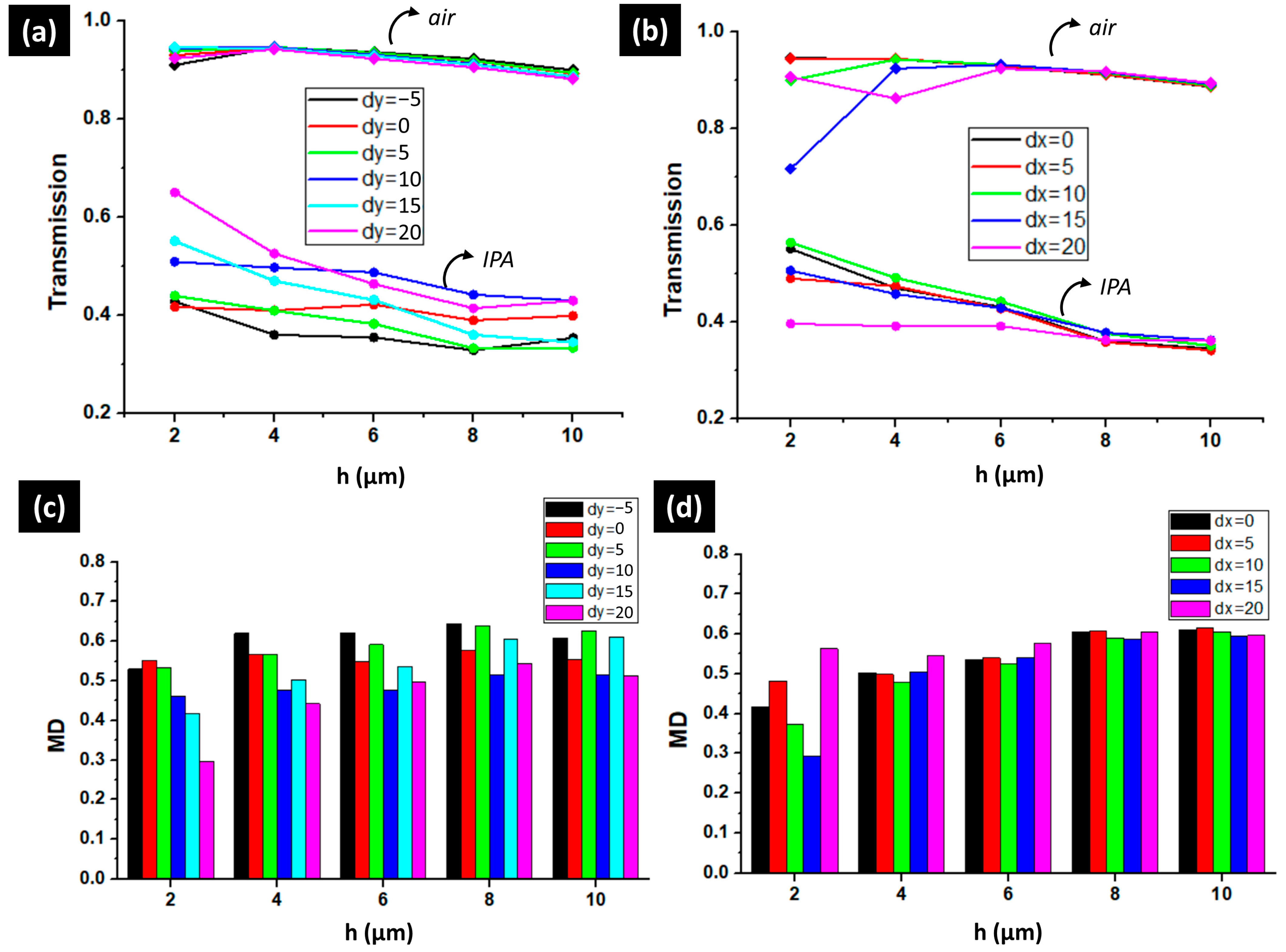
3.4. Impacts of h, Δx, and Δy on Amplitude Modulation of 2nd Resonance

From Figure 3c, it can be observed that liquids with an RI of 1.8 or greater are suitable interlayer media for amplitude modulation. When filled with such a liquid, the device exhibits a resonant dip, reducing the transmittance of THz waves (“off”-state). Conversely, evacuating the liquid eliminates the resonance and significantly increases the transmittance (“on”-state). To investigate this phenomenon, we examined two scenarios using IPA (n = 1.9) and water (n = 2.1) as interlayer media. Both Figure 6 (water) and Figure 7 (IPA) illustrate the relationships between the transmission amplitude at resonance, MD, and dimension parameters.
Firstly, in the absence of liquid, Figure 6a,b show that the transmission level decreases with an increasing substrate distance (h). This is due to the decrease in effective capacitance as the distance increases, leading to a blue shift of the first resonance at about 1.18 THz and a subsequent reduction in transmission at the frequencies of interest of about 1.78 THz. Notably, a weak Fano resonance appears when the device is highly asymmetric and coupling between layers is strong, as evidenced by the significantly reduced transmission at h = 2 μm for Δx ≥ 15 μm when the device is filled with air. In other cases, the transmission levels vary slightly with Δx and Δy. Specifically, they increase with decreasing Δy and increasing Δx, indicating improved “on”-state transmission at a given h when O-edges are close and SRRs are misaligned in the x-direction.
Regarding the resonance intensity when the device is filled with water, Figure 6a,b reveal that only weak resonance emerges at small substrate distances, exemplified by the case with h = 2 μm, Δx = 0, and Δy = 20 μm. Therefore, for use as an optical switch, h should be at least 4 μm or greater. Within this range, the influence of Δy on the resonance strength does not follow a clear pattern; however, the strength increases with increasing Δx. This is attributed to the intensification of the Fano resonance caused by structural asymmetry [51]. Considering these factors, Figure 6c,d confirm that when h is greater than 4 μm, the resulting MDs all reach satisfactory levels, and high MDs can be pursued by increasing Δx. The average MD for h ≥ 4 μm is 46.8%, with a maximum MD of 56.1% achieved at h = 4 μm, Δx = 20 μm, and Δy = 15 μm.
Next, we investigated IPA as the interlayer media. Notably, the resonant frequency remained almost constant for h ≥ 4 μm, regardless of variations in Δx and Δy. The average resonant frequency was 1.878 THz, with a standard deviation of 0.007. In contrast, when water was used, the average resonant frequency was 1.792 THz, with a standard deviation of 0.022. This suggests that an IPA-based optical switch is more tolerant to fabrication errors when considering frequency selectivity. Also, for this reason, the “on”-state transmission level remains almost constant at any given h, except when the weak Fano resonance appears at h = 2 μm and 4 μm for Δx ≥ 15 μm. In the absence of this occasional resonance, in Figure 7c, where Δx = 0, at a small substrate distance h, a high MD required the O-edges to be overlapping or in close proximity (small Δy). However, as h increased, this requirement became less necessary. On the contrary, unlike the water-based device, Δx did not significantly affect the MD in the IPA-based device. Consequently, for h ≥ 4 μm, the average MD was 56.1%, with a maximum MD of 64.5% achieved at h = 8 μm, Δx = 0 μm, and Δy = −5 μm.

4. Conclusions

In conclusion, we have reported a microfluidic device composed of two layers of planar THz metamaterials. Both layers can be easily fabricated by leveraging currently mature fabrication techniques. Through simulation, we have demonstrated the device’s exceptional sensing capabilities, achieving a sensitivity of up to 507.7 GHz/RIU for RI sensing and 16.03 GHz/μm as a pressure sensor. Furthermore, by simply injecting and evacuating water or IPA into/from the device, it can function as an optical switch with an MD as large as 64.5%. Simulation data have also shown that the device exhibits tolerance to fabrication errors during assembly, such as misalignment of the layers and imprecise control of the spacer thickness, for most applications. Strict alignment is only required when utilizing the second resonance for high-sensitivity RI sensing. The proposed microfluidic device holds promise for broader applications in fields such as biosensing, environmental monitoring, and optical communications, where its unique combination of sensitivity and tunability could lead to innovative solutions and advancements.

Author Contributions

Conceptualization, X.F. and M.Z.; methodology, M.Z.; software, X.F. and H.Y.; validation, H.Y. and H.-L.W.; formal analysis, M.Z. and Q.S.; investigation, H.-L.W. and Q.S.; resources, S.M.; data curation, H.-L.W. and S.M; writing—original draft preparation, M.Z.; writing—review and editing, X.F. and H.Y.; Visualization, Q.S.; supervision, M.Z.; project administration, M.Z.; funding acquisition, M.Z. All authors have read and agreed to the published version of the manuscript.

Funding

This research and the APC were both funded by the Natural Science Foundation of Shandong Province, grant number ZR2023MF064.

Data Availability Statement

The original contributions presented in this study are included in the article. Further inquiries can be directed to the corresponding author.

Conflicts of Interest

The authors declare no conflicts of interest.

Abbreviations

The following abbreviations are used in this manuscript:
THzterahertz
SRRsplit-ring resonator
RIrefractive index
IPAisopropyl alcohol
MDmodulation depth
FDTDfinite-difference time-domain
EMelectromagnetic
PMLperfectly matched layer
SDstandard deviation

References

  1. Chen, H.T.; Padilla, W.J.; Zide, J.M.; Gossard, A.C.; Taylor, A.J.; Averitt, R.D. Active terahertz metamaterial devices. Nature 2006, 444, 597–600. [Google Scholar] [CrossRef] [PubMed]
  2. Choi, M.; Lee, S.H.; Kim, Y.; Kang, S.B.; Shin, J.; Kwak, M.H.; Kang, K.Y.; Lee, Y.H.; Park, N.; Min, B. A terahertz metamaterial with unnaturally high refractive index. Nature 2011, 470, 369–373. [Google Scholar] [CrossRef] [PubMed]
  3. Lee, D.K.; Kang, J.H.; Kwon, J.; Lee, J.S.; Lee, S.; Woo, D.H.; Kim, J.H.; Song, C.S.; Park, Q.H.; Seo, M. Nano metamaterials for ultrasensitive Terahertz biosensing. Sci. Rep. 2017, 7, 8146. [Google Scholar] [CrossRef] [PubMed]
  4. Wang, Y.; Niu, J.; Jin, X.; Qian, X.; Xiao, C.; Wang, W. Molecularly Resonant Metamaterials for Broad-Band Electromagnetic Stealth. Adv. Sci. 2023, 10, 2301170. [Google Scholar] [CrossRef]
  5. Zhang, H.; Zhang, X.; Xu, Q.; Tian, C.; Wang, Q.; Xu, Y.; Li, Y.; Gu, J.; Tian, Z.; Ouyang, C.; et al. High-efficiency dielectric metasurfaces for polarization-dependent terahertz wavefront manipulation. Adv. Opt. Mater. 2018, 6, 1700773. [Google Scholar] [CrossRef]
  6. Saadeldin, A.S.; Hameed, M.F.O.; Elkaramany, E.M.; Obayya, S.S. Highly sensitive terahertz metamaterial sensor. IEEE Sens. J. 2019, 19, 7993–7999. [Google Scholar] [CrossRef]
  7. Yuan, G.; Rogers, K.S.; Rogers, E.T.; Zheludev, N.I. Far-field superoscillatory metamaterial superlens. Phys. Rev. Appl. 2019, 11, 064016. [Google Scholar] [CrossRef]
  8. Alrayes, N.; Hussein, M.I. Metamaterial-based sensor design using split ring resonator and Hilbert fractal for biomedical application. Sens. Bio-Sens. Res. 2021, 31, 100395. [Google Scholar] [CrossRef]
  9. Xiong, Z.; Shang, L.; Yang, J.; Chen, L.; Guo, J.; Liu, Q.; Danso, S.A.; Li, G. Terahertz sensor with resonance enhancement based on square split-ring resonators. IEEE Access 2021, 9, 59211–59221. [Google Scholar] [CrossRef]
  10. Han, J.; Lakhtakia, A. Semiconductor split-ring resonators for thermally tunable terahertz metamaterials. J. Mod. Opt. 2009, 56, 554–557. [Google Scholar] [CrossRef]
  11. Driscoll, T.; Andreev, G.O.; Basov, D.N.; Palit, S.; Cho, S.Y.; Jokerst, N.M.; Smith, D.R. Tuned permeability in terahertz split-ring resonators for devices and sensors. Appl. Phys. Lett. 2007, 91, 062511. [Google Scholar] [CrossRef]
  12. Zhu, M.; Lin, Y.S.; Lee, C. Coupling effect combined with incident polarization to modulate double split-ring-resonator in terahertz frequency range. J. Appl. Phys. 2014, 116, 173106. [Google Scholar] [CrossRef]
  13. Zhu, M.; Lee, C. A design of terahertz broadband filters and its effect in eliminating asymmetric characteristics in device structures. J. Light. Technol. 2015, 33, 3280–3285. [Google Scholar] [CrossRef]
  14. Zhu, M.; Lee, C. Facile metal transfer method for fabricating unconventional metamaterial devices. Opt. Mater. Express 2015, 5, 733–741. [Google Scholar] [CrossRef]
  15. Han, N.R.; Chen, Z.C.; Lim, C.S.; Ng, B.; Hong, M.H. Broadband multi-layer terahertz metamaterials fabrication and characterization on flexible substrates. Opt. Express 2011, 19, 6990–6998. [Google Scholar] [CrossRef]
  16. Linden, S.; Enkrich, C.; Wegener, M.; Zhou, J.; Koschny, T.; Soukoulis, C.M. Magnetic response of metamaterials at 100 terahertz. Science 2004, 306, 1351–1353. [Google Scholar] [CrossRef]
  17. Tao, H.; Chieffo, L.R.; Brenckle, M.A.; Siebert, S.M.; Liu, M.; Strikwerda, A.C.; Fan, K.; Kaplan, D.L.; Zhang, X.; Averitt, R.D.; et al. Metamaterials on paper as a sensing platform. Adv. Mater. 2011, 23, 3197. [Google Scholar] [CrossRef]
  18. Park, S.J.; Hong, J.T.; Choi, S.J.; Kim, H.S.; Park, W.K.; Han, S.T.; Park, J.Y.; Lee, S.; Kim, D.S.; Ahn, Y.H. Detection of microorganisms using terahertz metamaterials. Sci. Rep. 2014, 4, 4988. [Google Scholar] [CrossRef]
  19. Wang, W.; Yan, F.; Tan, S.; Zhou, H.; Hou, Y. Ultrasensitive terahertz metamaterial sensor based on vertical split ring resonators. Photonics Res. 2017, 5, 571–577. [Google Scholar] [CrossRef]
  20. Park, S.J.; Cha, S.H.; Shin, G.A.; Ahn, Y.H. Sensing viruses using terahertz nano-gap metamaterials. Biomed. Opt. Express 2017, 8, 3551–3558. [Google Scholar] [CrossRef]
  21. Meng, K.; Park, S.J.; Burnett, A.D.; Gill, T.; Wood, C.D.; Rosamond, M.; Li, L.H.; Chen, L.; Bacon, D.R.; Freeman, J.R.; et al. Increasing the sensitivity of terahertz split ring resonator metamaterials for dielectric sensing by localized substrate etching. Opt. Express 2019, 27, 23164–23172. [Google Scholar] [CrossRef] [PubMed]
  22. Zhu, M.; Chen, J.; Li, J. Selective trapping of micro-particles on terahertz metamaterial with macro gesture manipulation. J. Phys. D Appl. Phys. 2019, 52, 085104. [Google Scholar] [CrossRef]
  23. Rakhshani, M.R. Refractive index sensor based on dual side-coupled rectangular resonators and nanorods array for medical applications. Opt. Quantum Electron. 2021, 53, 232. [Google Scholar] [CrossRef]
  24. Rigamonti, G.; Bello, V.; Merlo, S. Spectral optical readout of rectangular–miniature hollow glass tubing for refractive index sensing. Sensors 2018, 18, 603. [Google Scholar] [CrossRef]
  25. Kuzin, A.; Panda, K.; Chernyshev, V.; Florya, I.; Kovalyuk, V.; An, P.; Golikov, A.; Chulkova, G.; Kolesov, D.; Gorin, D.; et al. Microfluidic–nanophotonic sensor for on-chip analysis of complex refractive index. Appl. Phys. Lett. 2024, 124, 063701. [Google Scholar] [CrossRef]
  26. Du, C.; Zhou, D.; Guo, H.H.; Pang, Y.Q.; Shi, H.Y.; Liu, W.F.; Su, J.Z.; Singh, C.; Trukhanov, S.; Trukhanov, A.; et al. An ultra-broadband terahertz metamaterial coherent absorber using multilayer electric ring resonator structures based on anti-reflection coating. Nanoscale 2020, 12, 9769–9775. [Google Scholar] [CrossRef]
  27. Wang, B.X.; Xu, C.; Duan, G.; Xu, W.; Pi, F. Review of broadband metamaterial absorbers: From principles, design strategies, and tunable properties to functional applications. Adv. Funct. Mater. 2023, 33, 2213818. [Google Scholar] [CrossRef]
  28. Pitchappa, P.; Manjappa, M.; Ho, C.P.; Qian, Y.; Singh, R.; Singh, N.; Lee, C. Active control of near-field coupling in conductively coupled microelectromechanical system metamaterial devices. Appl. Phys. Lett. 2016, 108, 111102. [Google Scholar] [CrossRef]
  29. Manjappa, M.; Pitchappa, P.; Singh, N.; Wang, N.; Zheludev, N.I.; Lee, C.; Singh, R. Reconfigurable MEMS Fano metasurfaces with multiple-input–output states for logic operations at terahertz frequencies. Nat. Commun. 2018, 9, 4056. [Google Scholar] [CrossRef]
  30. Tan, T.C.; Srivastava, Y.K.; Ako, R.T.; Wang, W.; Bhaskaran, M.; Sriram, S.; Al-Naib, I.; Plum, E.; Singh, R. Active control of nanodielectric-induced THz quasi-BIC in flexible metasurfaces: A platform for modulation and sensing. Adv. Mater. 2021, 33, 2100836. [Google Scholar] [CrossRef]
  31. Dong, Y.; Yu, D.; Li, G.; Lin, M.; Bian, L.A. Terahertz metamaterial modulator based on phase change material VO2. Symmetry 2021, 13, 2230. [Google Scholar] [CrossRef]
  32. Cong, L.; Srivastava, Y.K.; Zhang, H.; Zhang, X.; Han, J.; Singh, R. All-optical active THz metasurfaces for ultrafast polarization switching and dynamic beam splitting. Light Sci. Appl. 2018, 7, 28. [Google Scholar] [CrossRef] [PubMed]
  33. Sun, X.; Fu, Q.; Fan, Y.; Wu, H.; Qiu, K.; Yang, R.; Cai, W.; Zhang, N.; Zhang, F. Thermally controllable Mie resonances in a water-based metamaterial. Sci. Rep. 2019, 9, 5417. [Google Scholar] [CrossRef] [PubMed]
  34. Islam, M.S.; Sultana, J.; Biabanifard, M.; Vafapour, Z.; Nine, M.J.; Dinovitser, A.; Cordeiro, C.M.B.; Ng, B.H.; Abbott, D. Tunable localized surface plasmon graphene metasurface for multiband superabsorption and terahertz sensing. Carbon 2020, 158, 559–567. [Google Scholar] [CrossRef]
  35. Li, Y.; Chen, X.; Hu, F.; Li, D.; Teng, H.; Rong, Q.; Zhang, W.; Han, J.; Liang, H. Four resonators based high sensitive te-rahertz metamaterial biosensor used for measuring concentration of protein. J. Phys. D Appl. Phys. 2019, 52, 095105. [Google Scholar] [CrossRef]
  36. Aslinezhad, M. High sensitivity refractive index and temperature sensor based on semiconductor metamaterial perfect absorber in the terahertz band. Opt. Commun. 2020, 463, 125411. [Google Scholar] [CrossRef]
  37. Li, D.; Hu, F.; Zhang, H.; Chen, Z.; Huang, G.; Tang, F.; Lin, S.; Zou, Y.; Zhou, Y. Identification of early-stage cervical cancer tissue using metamaterial terahertz biosensor with two resonant absorption frequencies. IEEE J. Sel. Top. Quantum Electron. 2021, 27, 1–7. [Google Scholar] [CrossRef]
  38. Wang, Z.; Geng, Z.; Fang, W. Exploring performance of THz metamaterial biosensor based on flexible thin-film. Opt. Express 2020, 28, 26370–26384. [Google Scholar] [CrossRef]
  39. Lin, S.; Xu, X.; Hu, F.; Chen, Z.; Wang, Y.; Zhang, L.; Peng, Z.; Li, D.; Zeng, L.; Chen, Y.; et al. Using antibody modified terahertz metamaterial biosensor to detect concentration of carcinoembryonic antigen. IEEE J. Sel. Top. Quantum Electron. 2020, 27, 1–7. [Google Scholar] [CrossRef]
  40. Yao, H.; Mei, H.; Zhang, W.; Zhong, S.; Wang, X. Theoretical and experimental research on terahertz metamaterial sensor with flexible substrate. IEEE Photonics J. 2021, 14, 1–9. [Google Scholar] [CrossRef]
  41. Zhang, P.; Zhang, M.; Fu, Y.; Cai, H.; Zeng, X.; Chen, X.; Qiu, X.; Tian, Z.; Shi, S.; Yu, D.; et al. Design and Simulation of THz Metasurface Sensor Based on Transmission and Reflection Modes for Aqueous Solution Detection. Plasmonics 2024, 19, 1–11. [Google Scholar] [CrossRef]
  42. Liu, L.; Liu, Z.; Zhang, Y.; Liu, S. Side-polished D-type fiber SPR sensor for RI sensing with temperature compensation. IEEE Sens. J. 2021, 21, 16621–16628. [Google Scholar] [CrossRef]
  43. Dong, X.; Zeng, L.; Chu, D.; Sun, X. Highly sensitive refractive index sensing based on a novel Mach-Zehnder interferometer with TCF-PCF composite structure. Infrared Phys. Techn. 2022, 123, 104134. [Google Scholar] [CrossRef]
  44. Zhang, Y.; Lin, P.; Lin, Y.S. Tunable split-disk metamaterial absorber for sensing application. Nanomaterials 2021, 11, 598. [Google Scholar] [CrossRef] [PubMed]
  45. Shih, K.; Pitchappa, P.; Manjappa, M.; Ho, C.P.; Singh, R.; Lee, C. Microfluidic metamaterial sensor: Selective trapping and remote sensing of microparticles. J. Appl. Phys. 2017, 121, 023102. [Google Scholar] [CrossRef]
  46. Sun, H.; Hu, Y.; Tang, Y.; You, J.; Zhou, J.; Liu, H.; Zheng, X. Ultrafast polarization-dependent all-optical switching of germanium-based metaphotonic devices. Photon. Res. 2020, 8, 263–270. [Google Scholar] [CrossRef]
  47. He, W.; Tong, M.; Xu, Z.; Hu, Y.; Cheng, X.A.; Jiang, T. Ultrafast all-optical terahertz modulation based on an inverse-designed metasurface. Photon. Res. 2021, 9, 1099–1108. [Google Scholar] [CrossRef]
  48. Chen, X.; Tian, Z.; Lu, Y.; Xu, Y.; Zhang, X.; Ouyang, C.; Gu, J.; Han, J.; Zhang, W. Electrically tunable perfect terahertz absorber based on a graphene salisbury screen hybrid metasurface. Adv. Opt. Mater. 2020, 8, 1900660. [Google Scholar] [CrossRef]
  49. Xu, R.; Xu, X.; Yang, B.R.; Gui, X.; Qin, Z.; Lin, Y.S. Actively logical modulation of MEMS-based terahertz metamaterial. Photon. Res. 2021, 9, 1409–1415. [Google Scholar] [CrossRef]
  50. Hou, X.F.; Li, Y.Y.; Wu, X.J.; He, G.Y.; Wang, M.W. A thermal tunable terahertz metamaterial absorber based on strontium titanate. Phys. Scr. 2022, 97, 085507. [Google Scholar] [CrossRef]
  51. Singh, R.; Al-Naib, I.A.; Koch, M.; Zhang, W. Sharp Fano resonances in THz metamaterials. Opt. Express 2011, 19, 6312–6319. [Google Scholar] [CrossRef]
Figure 1. (a) Schematic of the microfluidic metamaterial device. (b) A unit cell of the device. (c) Top view of (b), highlighting the positioning of the metal SRRs in the unit cell. (d) Macroview of the assembled device under a normal THz incidence, illustrating the bonding area and the microfluidic chamber.
Photonics 12 00194 g001
Figure 2. (a) Transmission spectra of a typical device (h = 8 μm; Δx = 0; and Δy = 15 μm) when it is filled with air (black curve) or water (red curve). (b) Electromagnetic (EM) distribution maps of the typical device at the first (left column) and second resonances (right column) when filled with air or water. The x- and y-span in (b) both range from −40 to 40 μm. The color bar extends linearly from the minimum to the maximum value.
Photonics 12 00194 g002
Figure 3. (a) Transmission spectra of the typical device (with dimensions h = 8 μm; Δx = 0; and Δy = 15 μm) when it is filled with substances whose refractive indices range from 1.0 to 2.1. The color bar represents the normalized transmission amplitude. The dark and light blue regions are the corresponding resonant dips in each spectrum. (b) The linear relationship between the resonant frequencies and refractive index (RI) of the filling substance. Line curves showing (c) the shift of the first resonance and (d) the formation and shift of the second resonance in the transmission spectra.
Photonics 12 00194 g003
Figure 4. (a,b) show the relationship between the first resonant frequencies when the device is filled with air or water and the dimension parameters h, Δx, and Δy. In (a), Δx is fixed at 0. In (b), Δy is fixed at 15 μm. (c,d) are the calculated frequency shifts for each set of data in (a,b), respectively.
Photonics 12 00194 g004
Figure 5. (a,b) show the relationship between the second resonant frequencies when the device is filled with a substance of n = 1.8 or n = 2.1 and the dimension parameters h, Δx, and Δy. In (a), Δx is fixed at 0. In (b), Δy is fixed at 15 μm. (c,d) are the calculated frequency shifts for each set of data in (a,b), respectively.
Photonics 12 00194 g005
Figure 6. (a,b) show the relationship between the transmission level at the second resonance when the device is filled with air or water and the dimension parameters h, Δx, and Δy. In (a), Δx is fixed at 0. In (b), Δy is fixed at 15 μm. (c,d) are the calculated frequency shifts for each set of data in (a,b), respectively. The insets in (a,b) are the zoomed-in view of the data for air, with h ranging from 6 to 10 μm.
Photonics 12 00194 g006
Figure 7. (a,b) show the relationship between the transmission level at the second resonance when the device is filled with air or IPA and the dimension parameters h, Δx, and Δy. In (a), Δx is fixed at 0. In (b), Δy is fixed at 15 μm. (c,d) are the calculated frequency shifts for each set of data in (a,b), respectively.
Photonics 12 00194 g007
Table 1. Comparison of sensitivities of recently reported RI sensors and our typical device.
References[21][34][35][36][37][38][39][40][41]Our work
(before optimization)
Sensitivity (GHz/RIU)716685687424376.510066.7282 (1st resonance)
433 (2nd resonance)
References[23][24][25][42][43][44]Our work
(before optimization)
Sensitivity
(nm/RIU)
1090483.41382260226.735676.1 × 104~1.1 × 10⁵ (1st resonance)
3.6 × 10⁴~4.1 × 10⁴ (2nd resonance)
Table 2. Comparison of modulation depths (MDs) between recently reported THz metamaterial modulators and our typical device.
References[46][47][48][49][50]Our work
(before optimization)
MD (%)455025234060.7 (IPA)
56.3 (water)
Disclaimer/Publisher’s Note: The statements, opinions and data contained in all publications are solely those of the individual author(s) and contributor(s) and not of MDPI and/or the editor(s). MDPI and/or the editor(s) disclaim responsibility for any injury to people or property resulting from any ideas, methods, instructions or products referred to in the content.

