Article

Reflective Semiconductor Optical Amplifier Chip with Low Ripple for C-Band External Cavity Narrow-Linewidth Laser

1
School of Integrated Circuits, University of Chinese Academy of Sciences, Beijing 100083, China
2
Nanometer Optoelectronics Lab, Institute of Semiconductors, Chinese Academy of Sciences, Beijing 100083, China
*
Authors to whom correspondence should be addressed.
Photonics 2025, 12(3), 193; https://doi.org/10.3390/photonics12030193
Submission received: 27 January 2025 / Revised: 20 February 2025 / Accepted: 21 February 2025 / Published: 25 February 2025

Abstract

:
The main characteristic of a reflective semiconductor optical amplifier chip (RSOA) is that it does not generate optical resonance under electric pumping and maintains the operation state of spontaneous emission. In this paper, a Nb2O5/SiO2/Nb2O5/SiO2 (four-layer Nb2O5/SiO2) film system is employed as the coating material for the output facet of the RSOA. The 3 dB spectral width of the spontaneous emission spectrum from this RSOA reaches 79.4 nm, with a ripple of less than 1 dB occurring across this wavelength range. Notably, around the 1550 nm wavelength, the ripple is as low as 0.5 dB. This represents the best performance reported for this type of chip. The RSOA is packaged as a narrow-linewidth external cavity laser. Under test conditions of 25 °C and 180 mA, the external cavity laser produces an output power of 12.6 mW and achieves a linewidth of 299.8 Hz. Furthermore, by adjusting the Fabry–Pérot (FP) standard cavity, filtering, and other external cavity parameters, the lasing spectrum of the narrow-linewidth external cavity laser based on the RSOA is tunable across a wavelength range from 1535.83 nm to 1561.42 nm, which shows the usability of the proposed ROSA for a C-band external cavity narrow-linewidth laser.

1. Introduction

Since the advent of the information age, laser communication and laser sensing technologies have played pivotal roles in driving societal development and progress. The ITU-C band, positioned within both the optical fiber and atmospheric transmission windows, offers significant advantages, such as the low relative intensity noise (RIN), high gain, and high saturation amplification achievable with optical fiber amplifiers [1,2,3]. These characteristics make it one of the most widely used bands in various optical communication and sensing systems. Semiconductor lasers, with their compact size, light weight, high electro–optic efficiency, and ease of integration, are among the most utilized lasers in modern applications [4,5]. Laser linewidth is a critical parameter of semiconductor lasers, as it reflects the intensity of phase noise within the laser’s optical field [6,7,8,9,10]. Therefore, narrow-linewidth semiconductor lasers are frequently used in systems sensitive to source phase noise. For instance, in coherent optical communication, the laser linewidth influences the bit error rate and other performance metrics of phase modulation formats [9]. In laser sensing systems, the linewidth directly impacts the detection accuracy and sensitivity of the sensors [10]. Consequently, narrow-linewidth semiconductor lasers have become indispensable in modern information technologies and have been the focus of extensive research.
Narrow-linewidth external cavity lasers, owing to the ultra-high quality factor (often exceeding 106) of their external cavities [11], offer significant advantages in terms of linewidth reduction. For instance, external cavity lasers with a Littman configuration can achieve linewidths on the order of tens of kHz or even a few kHz, which are substantially narrower than the linewidths of DFB lasers, which are typically in the range of hundreds of kHz [12,13,14,15,16]. As a result, external cavity lasers have become the preferred solution for achieving narrow-linewidth performance. The RSOA, with its broad 3 dB spectral bandwidth and flexible wavelength selection, has found widespread application in narrow-linewidth external cavity lasers that require specific wavelength selection and tunability [8]. For example, semiconductor narrow-linewidth lasers based on an RSOA, combined with the Vernier effect achieved using dual micro-ring resonators (MRRs), have achieved a remarkable tuning range of 172 nm in the C + L band [17]. This broad tuning capability is enabled by the 3 dB spectral bandwidth of the RSOA. Therefore, further advancements in RSOA performance are crucial for the continued development of high-performance narrow-linewidth lasers.
The RSOA is a critical component in narrow-linewidth external cavity lasers. As the laser’s active medium, it enables lasing under electrical pumping, and thus plays a pivotal role, not only in determining the wavelength tuning range of the external cavity laser but also in influencing its output power and linewidth [18]. The ripple of the RSOA is a key factor in determining the linewidth of the narrow-linewidth laser [18]. Ripple, which represents the flatness index of the amplified spontaneous emission (ASE) spectrum of the RSOA, reflects the resonance strength of the FP cavity formed by the front and rear facets of the RSOA [19]. For external cavity lasers, the laser linewidth ideally should be governed by the external cavity, given the high quality factor, while any internal resonances from other cavities should be minimized [11]. This means that the ripple of the RSOA should be as low as possible, so that the optimal laser linewidth can be obtained. Extensive research has been conducted on RSOAs [20,21,22,23,24,25], with the lowest reported ripple being 1 dB; the lowest ripple for C-band RSOAs is typically around 2 dB. This limitation imposes constraints on further optimizing the linewidth of external cavity lasers. Consequently, reducing the ripple of the RSOA is of great significance for enhancing the linewidth of external cavity lasers, and thereby improving the performance of coherent optical communication systems and fiber-optic sensing applications.
In this paper, a four-layer Nb2O5 film system is designed as the coating material for the output facet of the ROSA. Under test conditions of 25 °C and 180 mA, the 3 dB spectral width of the RSOA’s spontaneous emission spectrum reaches 79.4 nm, spanning the wavelength range from 1497.2 nm to 1576.6 nm. Within this range, the ripple is maintained at less than 1 dB, with the ripple near 1550 nm being approximately 0.5 dB. To the best of our knowledge, this represents the best performance reported to date. The narrow-linewidth external cavity laser fabricated with this RSOA achieves a linewidth of 299.8 Hz at 180 mA, while maintaining an output power of 12.6 mW at room temperature (25 °C). Furthermore, by adjusting parameters such as the FP standard cavity and filtering within the external cavity, the lasing spectrum of an external cavity laser constructed with this RSOA can cover wavelengths from 1535.83 nm to 1561.42 nm. This capability holds significant practical value for the realization of narrow-linewidth lasers with a broad tuning range.

2. Design and Fabrication

2.1. Wide-Spectrum, Low-Reflectance Coating Design

The key to achieving high-performance in an RSOA lies in ensuring that the output end facet exhibits an extremely low reflectance. To maintain stable operating conditions for the RSOA, the reflectance of the output end facet should ideally be on the order of 10−5 [23,26,27,28]. Achieving such low reflectance requires careful selection of coating materials and precise optimization of the coating layer thickness on the output end facet. TiO2 and Nb2O5 thin films are widely used in optical multilayer coatings due to their excellent optical transmittance in the visible and near-infrared wavelength ranges, as well as their high refractive indices [29,30,31]. Extensive research has been conducted on the structure, optical properties, and fabrication conditions of TiO2 and Nb2O5 films, aiming to produce high-quality optical coatings [32,33,34,35,36,37,38,39,40,41]. It has been observed that amorphous materials are typically preferred for the multilayer optical films on facets. TiO2 films, however, exhibit poor refractive index stability during fabrication and significant absorption, which further increases under ultraviolet exposure. Additionally, at a 300 °C annealing condition, TiO2 films undergo a transition from an amorphous to a crystalline state, which facilitates the formation of a crystalline structure during fabrication. In contrast, Nb2O5 films offer better chemical stability compared to TiO2. The transition temperature from the amorphous to crystalline state for Nb2O5 films is above 450 °C, making it relatively easier to prepare high-quality amorphous Nb2O5 films. After careful comparison, Nb2O5/SiO2 multilayer coatings were ultimately selected as the film layer for the RSOA, as they provide a broadband, low-reflectance solution.
There have been numerous reports on optimizing the parameters of low-reflection coatings for the end facet [42,43,44,45]. For multilayer coating structures [46], the effective interface method is commonly used for calculations. Any optical multilayer structure can be replaced by a virtual equivalent interface, which allows the characteristics of a single-layer film to be extended to the multilayer case [46].
Taking a single-layer film with an exit medium of air as an example, the reflectance is given as described in [46]:
R = n 0 - n R 2 cos 2 δ 1 + n R n 0 n f - n f 2 sin 2 δ 1 n 0 + n R 2 cos 2 δ 1 + n R n 0 n f + n f 2 sin 2 δ 1
δ 1 =   2 π λ n f d cos θ 1
where R is the optical intensity reflectance; nR is the refractive index of the incident medium, i.e., the refractive index of the waveguide mode; nf is the refractive index of the film material; n0 is the refractive index of the surrounding medium, generally referring to air; δ1 is the phase thickness; d is the film thickness; and θ1 is the incidence angle.
When the refractive index of the film layer is designed to lie between that of the incident medium and air, the single-layer film exhibits anti-reflection properties. Under the conditions of normal incidence of light and where the optical thickness nfd = λ/4, the reflectance is given as follows:
R = n R - 1 2 cos 2 2 π λ × λ 4 + n R n f - n f 2 sin 2 2 π λ × λ 4 n R + 1 2 cos 2 2 π λ × λ 4 + n R n f + n f 2 sin 2 2 π λ × λ 4 = n R - n f 2 2 n R + n f 2 2
When nf equals the square root of nR, the reflectance is zero, i.e., complete transmission occurs.
When employing the effective interface method [46] for calculations, in the case of a multilayer thin-film structure under normal incidence, the interface reflection coefficient ri and transmission coefficient ti for the i layer are given by
r i = n i 1 - n i n i 1 + n i
t i = 2 n i 1   n i 1 + n i
where ni is the refractive index of the i layer. For the i layer, the effective reflection coefficient (Ri) is given by:
R i = r i + t i 2 R i + 1 e 2 i δ i 1 r i R i + 1 e 2 i δ i  
δ i = 2 π λ n f d c o s θ i
By recursively calculating up to the first layer, the total reflection coefficient (R1) of the multilayer film is obtained, and the total reflectance R is given by
R = R 1 2
Based on the aforementioned theory, the coating layers for the output facet of the RSOA are simulated. Figure 1a shows a simulated diagram of the reflection spectrum of the output facet of the RSOA. For RSOA chips, it is best to maintain the reflectivity of the output facet at the level of 10−5 [23]. The reflection spectrum of the Nb2O5/SiO2 multilayer is V-shaped, as indicated by the blue line in Figure 1a. From the blue line in Figure 1a, it can be seen that the wavelength range where the reflection coefficient of the Nb2O5/SiO2 multilayer is below 1 × 10⁻⁵ only covers 1534–1546 nm, a 12 nm range, which does not meet the requirement of covering the C-band from 1530 nm to 1565 nm. Therefore, the low-reflectance bandwidth of the Nb2O5/SiO2 multilayer is relatively narrow, making it unsuitable for creating a wideband low-reflectance coating for the C-band. To address this limitation, a four-layer Nb2O5/SiO2 film system is simulated which broadens the reflection bandwidth and provides a wide-spectrum, low-reflectance coating, as shown by the pink line in Figure 1a. For the four-layer Nb2O5/SiO2 film system, the wavelength range where the reflection coefficient is below 1 × 10⁻⁵ spans from 1498 nm to 1582 nm, covering a total of 84 nm, covering the C-band. Thus, to achieve a wideband low-reflectance spectrum for the RSOA, the four-layer Nb2O5/SiO2 film system is adopted. The thicknesses of the layers in the four-layer Nb2O5 film system are Nb2O5/SiO2/Nb2O5/SiO2 = 223.61 nm/168.44 nm/105.57 nm/341.49 nm, and they are labeled as the first layer to the fourth layer, respectively.
Figure 1b illustrates the variations in reflectivity in a four-layer Nb2O5/SiO2 film system when the thickness of each individual layer is varied by 1 nm. For the Nb2O5 layers, a variation of 1 nm in the thickness of the first high-refractive-index layer results in a wavelength range, with reflectivity value below 1 × 10⁻⁵, extending from 1570 nm to 1583 nm, and the reflective bandwidth is only 13 nm, as shown by the red line in Figure 1b. Similarly, for the third layer, the corresponding wavelength range, with reflectivity below 1 × 10⁻⁵, shifts to 1536–1569 nm, as shown by the pink line in Figure 1b. These results indicate that for the Nb2O5 layers, the reflective bandwidth changes significantly with thickness variations. In contrast, for the low-refractive-index SiO2 layers, changing the thicknesses of the second layer and the fourth layer by 1 nm leads to reflection bandwidths, with reflectivity below 1 × 10⁻⁵, of 50 nm to 75 nm, as shown by the blue and green lines in Figure 1b, respectively. These findings suggest that for the SiO2 layers, a 1 nm variation limit for thickness ensures full coverage of the C-band (1530–1565 nm). As shown in Figure 1b, the thickness precision requirements for the Nb2O5 layers are more stringent than those for the SiO2 layers. The variation in the thickness of the Nb2O5 layers has a significant impact on the reflection bandwidth as compared to the SiO2 layers. However, the reflection bandwidth parameters are critical for determining whether narrow-linewidth lasers can achieve a wide tuning range. To achieve precise control over reflectivity and larger reflective bandwidth, the design precision is set at 0.01 nm, while the coating equipment control precision is maintained at 0.1 nm.

2.2. Fabrication of the RSOA

The schematic of the RSOA structure is shown in Figure 2, with the names of each part of the epitaxial structure marked in black font. From bottom to top, the epitaxial structure of the device includes the N-type InP substrate, N-InP cladding layer, lower waveguide layer, quantum well active region, upper waveguide layer, P-InP cladding layer, and InGaAs ohmic contact layer. The active region consists of three strained InGaAsP quantum wells, each with an 8 nm thickness. The use of aluminum-free InGaAsP for the active region helps to extend the lifespan of the RSOA.
To achieve stable spontaneous emission in the RSOA, in addition to depositing a coating layer with extremely low reflectance on the output facet, the optical waveguide can also be designed with an inclined or curved shape [47]. According to Reference [48], the light-emission angle of the RSOA chip is 7°. The completed chip is shown under a microscope in Figure 3. During the fabrication of the RSOA, a double-ridge waveguide structure, as illustrated in Figure 2, was formed using photolithography and etching processes, with an etching depth of 2.1 µm. A 300 nm SiO2 insulating layer was then deposited over the entire upper surface of the chip using plasma-enhanced chemical vapor deposition (PECVD). Through photolithography and etching, the SiO2 dielectric layer above the ridge waveguide was removed to form the electrical injection window. The P-side metal layer (Ti/Pt/Au) was deposited via magnetron sputtering. The substrate was subsequently thinned to approximately 140 µm and metallized. Finally, the facet coatings of the RSOA were completed using cleaving and sputtering processes. A wideband low-reflectance coating was applied to the front facet, while a high-reflection coating was applied to the rear facet.

3. Results and Discussion

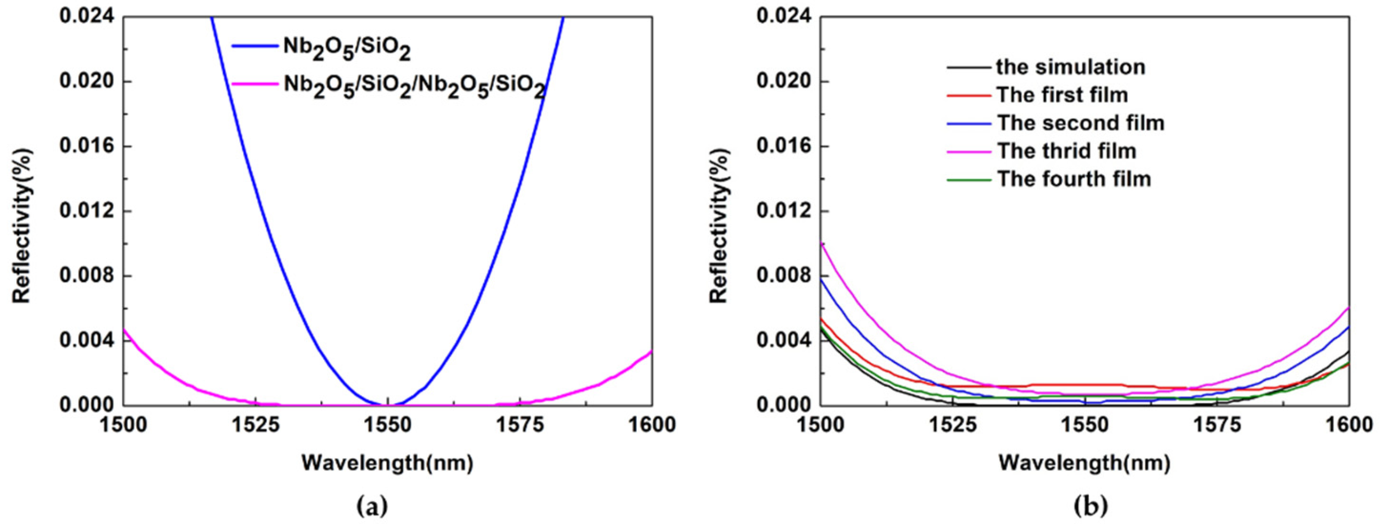
3.1. Analysis of the Test Results of the Wideband Low-Reflectance Coating

Due to the small facet size of the RSOA, it is not feasible to directly measure the reflectance of the chip’s facet using instruments such as a spectrophotometer or ellipsometer. Therefore, the wideband low-reflectance coating on the RSOA chip’s output facet is equivalently characterized by testing the transmittance of K9 glass samples from the same batch. Figure 4 compares the test results of the four-layer Nb2O5/SiO2 film system with the simulated results. The blue line in Figure 4 represents the simulated result of the four-layer Nb2O5/SiO2 film system, which is derived from the multi-layer film structure model [46]. We incorporate the simulated thickness into the model, where the refractive index is adjusted from that of the incident medium to the refractive index of K9 glass. The reflectivity of this film system on the K9 glass substrate is obtained through calculation. The red line in Figure 4 represents the experimental results of the four-layer Nb2O5/SiO2 film system, as obtained from the transmittance curve of the K9 glass sample after coating, and measured using a spectrophotometer. As can be observed in Figure 4, within the wavelength range of 1500–1600 nm, the experimental values for the K9 glass sample closely match the simulated results. The refractive index of the single layer has been calibrated using a spectrophotometer. The thickness of the four-layer Nb2O5/SiO2 thin-film system was determined based on the measured red line in Figure 4 according to the multi-layer film structure model [46]. The layer thicknesses are as follows: Nb2O5/SiO2/Nb2O5/SiO2 = 223.62 nm/169.11 nm/105.56 nm/342.85 nm. Compared to the simulated values, the deviation in Nb2O5 thickness is negligible, while the deviation in SiO2 thickness is only 1 nm. As shown in Figure 1b, a thickness precision of 1 nm is sufficient for the fourth layer to meet the required optical performance standards.

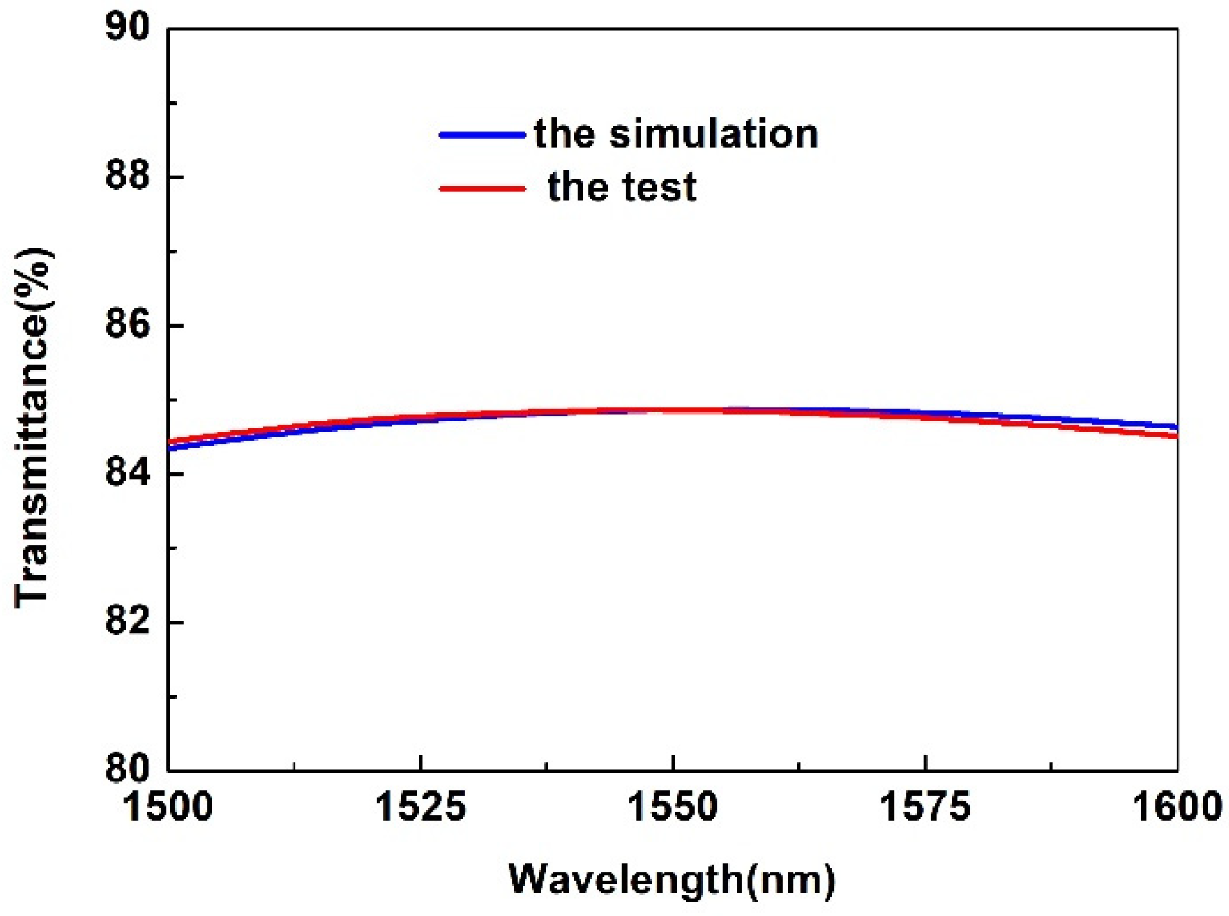
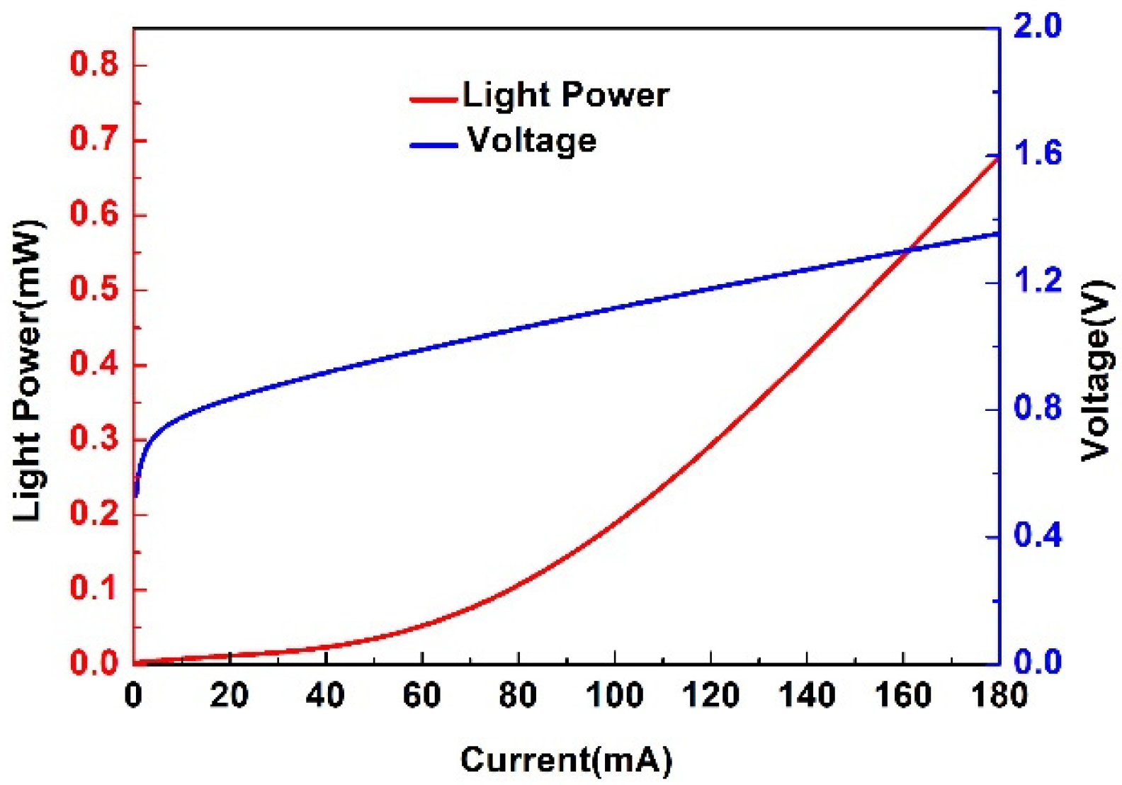
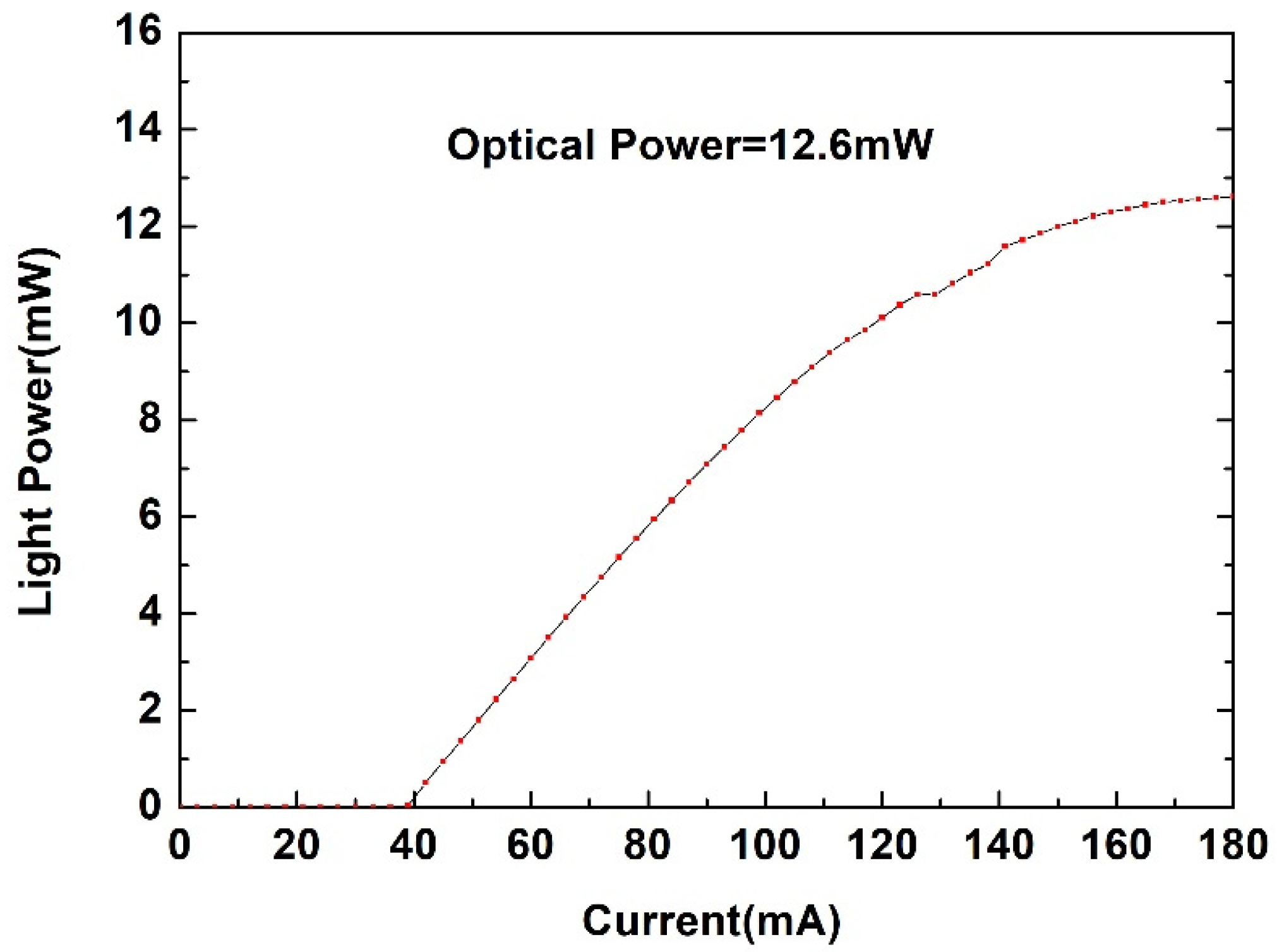
3.2. Analysis of Light–Current (L-I), Voltage–Current (V-I), and Spectral Test Results

After completing the accuracy tests and verification for the coating, the PIV characteristics of the fabricated RSOA were first tested to observe whether it operates as a spontaneous emission chip. The test conditions for the RSOA were set to room temperature (25 °C), with an injection current of 180 mA. The test results are shown in Figure 5. From Figure 5, it can be seen that under the test conditions of 25 °C and 180 mA, the output optical power of the chip is 0.67 mW, the operating voltage is 1.35 V, and the differential resistance of the chip is 2.4 Ω. The light–current (L-I) curve in Figure 5 shows that the RSOA has not yet reached lasing and is still in the spontaneous emission state. This is attributed to the use of the bent waveguide structure and the low-reflectance coating on the facet, which effectively suppresses optical feedback from the chip’s intrinsic FP cavity.
Next, the spectrum of the RSOA was measured to study the effects of the reflectance coating on the RSOA’s spontaneous emission spectrum, including the 3 dB spectral width and ripple. Firstly, the RSOA chip was connected to a TEC (thermoelectric cooler). Following this, the RSOA chip was powered on, and its operating temperature was controlled. Then, a collimating lens was employed to carry out the coupling process for the RSOA chip. Lastly, a polarization-maintaining fiber was used to couple the output light from the chip into the fiber, which was then connected to a spectrometer for spectral analysis. The test results are shown in Figure 6.
Figure 6a presents the spectral output of the RSOA with the four-layer Nb2O5/SiO2 film system on the output facet. Under the test conditions of 25 °C and 180 mA, the 3 dB spectral width of the RSOA’s spontaneous emission spectrum is approximately 79 nm, covering a wavelength range from 1497.2 to 1576.6 nm. The simulated results in Figure 1 indicate that within the wavelength range of 1498–1582 nm, the reflectance of the RSOA is below 1 × 10⁻⁵. The test results in Figure 6a closely match the simulated values from Figure 1, confirming that within the wavelength range of 1497.2–1576.6 nm, the RSOA is operating in a low-reflectance state. Furthermore, within this 3 dB spectral-width range, the ripple is less than 1 dB, as shown in Figure 6a. Figure 6b presents the amplified spontaneous emission (ASE) spectrum within the 1548–1552 nm wavelength range. Within this narrow range, the ripple of the RSOA is approximately 0.5 dB. Extensive research has been conducted on RSOAs [20,21,22,23,24,25], with the lowest previously reported ripple being 1 dB, while C-band RSOAs typically exhibit a minimum ripple of around 2 dB. The ripple observed in this RSOA represents the best performance reported to date. This performance is primarily attributed to the implementation of the four-layer Nb2O5/SiO2 film system in conjunction with a bent waveguide structure. This design suppressed the optical feedback from the FP cavity of the RSOA, effectively lowering the ripple associated with the chip’s intrinsic resonance to a new level, and achieved a very low output facet reflectivity. Furthermore, as observed in Figure 6, the ripple intensity varies slightly at different wavelengths. This is attributed to the fact that the reflection of the output facet of the RSOA cannot be entirely suppressed, and the RSOA’s intrinsic FP cavity exhibits certain resonance effects. Therefore, achieving extremely low reflectivity at the light-emitting facet is crucial for optimizing the performance of the RSOA.

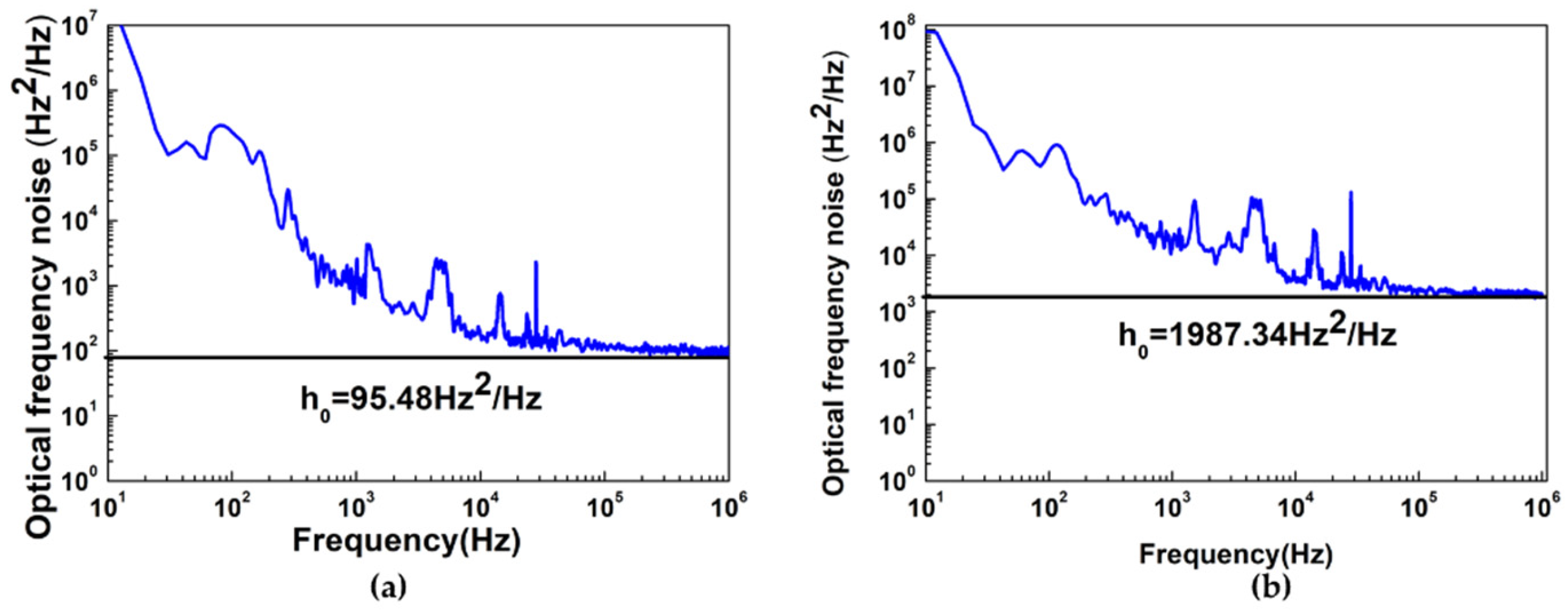
3.3. Analysis of Narrow-Linewidth Laser Test Results

After completing the tests of the RSOA’s spontaneous emission spectrum and ripple, the impact of the ultra-low ripple of the four-layer Nb2O5/SiO2 film system on the narrow-linewidth laser is investigated. To this end, a narrow-linewidth external cavity laser is designed. The external cavity structure integrates the FP standard cavity and filtering and optical feedback devices. The structural schematic of the system is shown in Figure 7.
The linewidth of the laser is measured, and the output power of different currents is measured using an optical power meter. The test results are shown in Figure 8 and Figure 9. Figure 8 presents the power spectral density (PSD) of frequency noise of a narrow-linewidth laser utilizing the RSOA chip under test conditions of 25 °C and 180 mA. It is noted that the frequency noise spectral density exhibits a constant level h0 (Hz2/Hz) below a cutoff frequency (fc). In this case, the laser linewidth can be approximated as πh0 [49]. As shown in Figure 8a, the extracted value of h0 is 95.48 Hz2/Hz, leading to a calculated linewidth of 299.8 Hz for the narrow-linewidth laser produced by the RSOA with a normal wide-spectrum, low-reflectance coating. Figure 8b presents the test results of a narrow-linewidth laser fabricated using an RSOA chip with a less preferable wide-spectrum, low-reflectance coating (reflectance ≈ 1 × 10⁻⁴) under the same external cavity conditions and testing environment. From Figure 8b, it is evident that the linewidth of the laser produced by the chip with an inferior wide-spectrum, low-reflectance coating is significantly broader, measuring 6240.2 Hz. Therefore, the quality of the wide-spectrum, low-reflectance coating impacts the linewidth of the laser.
This narrow linewidth is attributed to the low ripple in the RSOA, which significantly optimizes the linewidth of the external cavity laser [18]. Figure 9 presents the light–current (L-I) curve of the narrow-linewidth laser. It can be observed that, under a test current of 180 mA, the narrow-linewidth laser made with the RSOA chip has an output power of 12.6 mW, with a threshold current around 40 mA. These results confirm that the linewidth of the narrow-linewidth laser produced by the RSOA, using the four-layer Nb2O5/SiO2 film system, reaches the sub-kHz level while maintaining a certain output power, indicating relatively high performance.
Finally, by adjusting the FP standard cavity, filtering, and other parameters of the external cavity, a wide wavelength-tuning range is achieved for the narrow-linewidth laser. The tuning range spans from 1535.83 nm to 1561.42 nm, as shown in Figure 10. This demonstrates that an RSOA with an ultra-low ripple from the four-layer Nb2O5/SiO2 film system can be effectively applied to narrow-linewidth lasers requiring a wide tuning range. The four-layer Nb2O5/SiO2 film system provides a wide-spectrum, low-reflectance coating, enabling flexible wavelength selection over a large wavelength range.

4. Conclusions

This paper introduces a four-layer Nb2O5/SiO2 film system which has been successfully applied to develop an RSOA chip with a wide-spectrum, low-reflectance output facet. The RSOA, utilizing this film system, exhibits a 3 dB spectral width of 79.4 nm in its spontaneous emission spectrum, covering a wavelength range from 1497.2 nm to 1576.6 nm. Within this range, the ripple is kept below 1 dB, with the ripple near 1550 nm reaching as low as 0.5 dB, which represents the best reported performance to date. To assess the practical performance of this RSOA chip, it is packaged into a narrow-linewidth external cavity laser. Under the test conditions of 25 °C and 180 mA, the external cavity laser demonstrates a linewidth of 299.8 Hz and an output power of 12.6 mW. By adjusting the FP standards, filters, and other parameters of the external cavity, the lasing wavelength ranges from 1535.83 nm to 1561.42 nm. This research significantly advances the field of external cavity lasers, offering new possibilities for wide-tuning and narrow-linewidth applications.

Author Contributions

Conceptualization, S.L., Z.L. and Y.C.; methodology, S.L., M.R. and H.B.; validation, S.L., Z.L., Y.C. and H.Y.; writing—original draft preparation, S.L.; writing—review and editing, S.L., Z.L., Y.C. and H.Y.; project administration, J.L. and Y.C. All authors have read and agreed to the published version of the manuscript.

Funding

This research was funded by the National Key Research and Development Program of China, funding number 62035009.

Institutional Review Board Statement

Not applicable.

Informed Consent Statement

Not applicable.

Data Availability Statement

Data is contained within the article.

Acknowledgments

The authors are grateful to the Nanometer Optoelectronics Lab, Institute of Semiconductors, Chinese Academy of Sciences; and the School of Integrated Circuits, University of Chinese Academy of Sciences.

Conflicts of Interest

The funders had no role in the design of the study; in the collection, analyses or interpretation of data; in the writing of the manuscript; or in the decision to publish the results.

References

  1. Seimetz, M. Laser linewidth limitations for optical systems with high-order modulation employing feed-forward digital carrier phase estimation. In Proceedings of the OFC/NFOEC 2008, San Diego, CA, USA, 24–28 February 2008. [Google Scholar]
  2. Tang, L.; Jia, H. Hybrid integrated low-noise linear chirp frequency-modulated continuous-wave laser source based on self-injection to an external cavity. Photonics Res. 2021, 9, 1948–1957. [Google Scholar] [CrossRef]
  3. Labaziewicz, J.; Richerme, P. Compact, filtered diode laser system for precision spectroscopy. Opt. Lett. 2007, 32, 572–574. [Google Scholar] [CrossRef] [PubMed]
  4. Gravel, B. Evaluation of a compact high power pulsed fiber laser source for laser-induced breakdown spectroscopy. J. Anal. At. Spectrom. 2011, 26, 1354–1361. [Google Scholar] [CrossRef]
  5. Wright, M.W.; Franzen, D. Qualification and reliability testing of a commercial high-power fiber-coupled semiconductor laser for space applications. Opt. Eng. 2005, 44, 054204. [Google Scholar] [CrossRef]
  6. Seimetz, M.; Molle, L. Coherent RZ-8PSK transmission at 30 Gbit/s over 1200 km employing homodyne detection with digital carrier phase estimation. In Proceedings of the 33rd European Conference and Exhibition of Optical Communication, Berlin, Germany, 16–20 September 2007. [Google Scholar]
  7. Schawlow, A.L.; Townes, C.H. Infrared and Optical Masers. Phys. Rev. 1958, 112, 1940–1949. [Google Scholar] [CrossRef]
  8. Henry, C. Theory of the linewidth of semiconductor lasers. I IEEE J. Quantum Electron. 1982, 18, 259–264. [Google Scholar] [CrossRef]
  9. Zediker, M.S.; Boucart, J. Eye safe high power laser diode in the 1410–1550 nm range. In Proceedings of the High-Power Diode Laser Technology and Applications VIII, San Francisco, CA, USA, 25–26 February 2010. [Google Scholar]
  10. Emmanuel, J.C.; Eldar, Y.C. Compressed Sensing with Coherent and Redundant Dictionaries. Appl. Comput. Harmon. Anal. 2011, 31, 59–73. [Google Scholar]
  11. Lang, R.; Kobayashi, K. External optical feedback effects on semiconductor injection laser properties. IEEE J. Quantum Electron. 1980, 16, 347–355. [Google Scholar] [CrossRef]
  12. Hoppe, M.; Rohling, H. New wide tunable external cavity interband cascade laser based on a micro-electro-mechanical system device. In Proceedings of the MOEMS and Miniaturized Systems XVIII, San Francisco, CA, USA, 2–4 March 2019. [Google Scholar]
  13. Hou, L.; Haji, M. Narrow linewidth laterally coupled 1.55 µm AlGaInAs/InP distributed feedback lasers integrated with a curved tapered semiconductor optical amplifier. Opt. Lett. 2012, 37, 4525–4527. [Google Scholar] [CrossRef]
  14. Wang, Z.; Shang, J. All-Polarization Maintaining Single-Longitudinal-Mode Fiber Laser with Ultra-High OSNR, Sub-kHz Linewidth and Extremely High Stability. Opt. Laser Technol. 2021, 141, 107135. [Google Scholar] [CrossRef]
  15. Liu, Y.; Zhang, M. Single-Longitudinal-Mode Triple-Ring Brillouin Fiber Laser with a Saturable Absorber Ring Resonator. J. Light. Technol. 2017, 35, 1744–1749. [Google Scholar] [CrossRef]
  16. Voo, N.Y.; Horak, P. Anomalous linewidth behavior in short-cavity single-frequency fiber lasers. IEEE Photonics Technol. Lett. 2005, 17, 546–548. [Google Scholar] [CrossRef]
  17. Guo, Y.; Li, X. Hybrid integrated external cavity laser with a 172-nm tuning range. APL Photonics 2022, 7, 066101. [Google Scholar] [CrossRef]
  18. Riehle, F. Frequency Standards: Basics and Applications; John Wiley & Sons, Inc.: Hoboken, NJ, USA, 2006. [Google Scholar]
  19. Kim, H.S.; Choi, B.S. Improvement of modulation bandwidth in multisection RSOA for colorless WDM-PON. Opt. Express 2009, 17, 16372–16378. [Google Scholar] [CrossRef] [PubMed]
  20. Parolari, P. 10-Gb/s Operation of a Colorless Self-Seeded Transmitter Over More Than 70 km of SSMF. IEEE Photonics Technol. Lett. 2014, 26, 599–602. [Google Scholar] [CrossRef]
  21. Parolari, P.; Marazzi, L. C- and O-Band Operation of RSOA WDM PON Self-Seeded Transmitters up to 10 Gb/s. J. Opt. Commun. Netw. 2015, 7, A249–A255. [Google Scholar] [CrossRef]
  22. Taebi, S.; Saini, S.S. L-Band Polarization-Independent Reflective SOA for WDM-PON Applications. IEEE Photonics Technol. Lett. 2009, 21, 334–336. [Google Scholar] [CrossRef]
  23. Kelly, A.E. High performance polarisation independent reflective semiconductor optical amplifiers in the S, C, and L bands. IEEE J. Sel. Areas Commun. 2010, 28, 943–948. [Google Scholar] [CrossRef]
  24. Valicourt, G.d.; Maho, A. Novel bidirectional reflective semiconductor optical amplifier. In Proceedings of the 2016 21st OptoElectronics and Communications Conference, Niigata, Japan, 3–7 July 2016. [Google Scholar]
  25. Valicourt, G.d. Radio-Over-Fiber Access Network Architecture Based on New Optimized RSOA Devices With Large Modulation Bandwidth and High Linearity. IEEE Trans. Microw. Theory Tech. 2010, 58, 3248–3258. [Google Scholar] [CrossRef]
  26. Alphonse, G.A. Design of high-power super luminescent diodes with low spectral modulation. In Proceedings of the SPIE 2002, San Jose, CA, USA, 19–25 January 2002. [Google Scholar]
  27. Ghafouri-Shiraz, H. Analysis of facet reflectivity, mirror loss, single-transverse mode condition and beam divergence angle at 1.3 pm and 1.55 pm wavelength of InGaAsP/InP buried heterostructure semiconductor laser diodes. Opt. Laser Technol. 1990, 22, 38–46. [Google Scholar] [CrossRef]
  28. Jaskorzynska, B.; Nilsson, M.J. reflectivity of uptapered, tilted-facet, and antireflection-coated di-ode-laser amplifiers. J. Opt. Soc. Am. B 1991, 8, 484–493. [Google Scholar] [CrossRef]
  29. Rani, R.A.; Zoolfakar, A. Thin films and nanostructures of niobium pentoxide: Fundamental properties, synthesis methods and applications. J. Mater. Chem. A 2014, 2, 15683–15703. [Google Scholar] [CrossRef]
  30. Nico, C.; Monteiro, T. Niobium oxides and niobates physical properties: Review and prospects. Prog. Mater. Sci. 2016, 80, 1–37. [Google Scholar] [CrossRef]
  31. Chen, K.N.; Hsu, C.M. Investigation of antireflection Nb2O5 thin films by the sputtering method under different deposition parameters. Micromachines 2016, 7, 151. [Google Scholar] [CrossRef] [PubMed]
  32. Horprathum, M.; Eiamchai, P. Structural, optical and hydrophilic properties of nanocrystalline TiO2 ultra-thin films prepared by pulsed dc reactive magnetron sputtering. J. Alloys Compd. 2011, 509, 4520–4524. [Google Scholar] [CrossRef]
  33. Tian, G.; He, H. Effect of microstructure of TiO2 thin films on optical band gap energy. Chin. Phys. Lett. 2005, 22, 1787–1789. [Google Scholar]
  34. Wang, W.-H.; Chao, S. Annealing effect on ion- beam—Sputtered titanium dioxide film. Opt. Lett. 1998, 23, 1417–1419. [Google Scholar] [CrossRef]
  35. Zhao, Z.; Tay, B.K. Room-temperature deposition of amorphous titanium dioxide thin film with high refractive index by a filtered cathodic vacuum arc technique. Appl. Opt. 2004, 43, 1281–1285. [Google Scholar] [CrossRef]
  36. Asanuma, T.; Matsutani, T. Structural and optical properties of titanium dioxide films deposited by reactive magnetron sputtering in pure oxygen plasma. J. Appl. Phys. 2004, 95, 6011–6016. [Google Scholar] [CrossRef]
  37. Sun, L.; Hou, P. Spectroscopic ellipsometry study one-beam deposited titanium dioxide films. Thin Solid Films 2004, 455–456, 525–529. [Google Scholar] [CrossRef]
  38. Bennett, J.M.; Pelletier, E. Comparison of the properties of titanium dioxide films prepared by various technique. Appl. Opt. 1989, 28, 3303–3317. [Google Scholar] [CrossRef] [PubMed]
  39. Venkataraj, S.; Drese, R. Temperature stability of sputtered niobium—Oxide films. J. Appl. Phys. 2002, 91, 4863–4871. [Google Scholar] [CrossRef]
  40. Lee, C.; Tien, C. Internal stress and optical properties of Nb2O5 thin films deposited by ion—Beam sputtering. Appl. Opt. 2002, 41, 2043–2047. [Google Scholar] [CrossRef]
  41. Lai, F.; Li, M. Optical scattering characteristic of annealed niobium oxide films. Thin Solid Film. 2005, 488, 314–320. [Google Scholar] [CrossRef]
  42. Hellmich, W.; Deimel, P.P. Optimal AR-coating for optical waveguide devices. J. Light. Technol. 1992, 10, 469–476. [Google Scholar] [CrossRef]
  43. Kendall, P.C.; Roberts, D.A. Semiconductor laser facet reflectivities using free-space radiation modes. IEEE Proc. J. Optoelectron. 1993, 1, 49–55. [Google Scholar] [CrossRef]
  44. Saitoh, T.; Mukai, T. Theoretical analysis and fabrication of antireflection coatings on laser-diode facets. J. Light. Technol. 1985, 3, 288–293. [Google Scholar] [CrossRef]
  45. Vassallo, C. Theory and practical calculation of antireflection coatings on semiconductor laser diode optical amplifiers. IEEE Proc. J. Optoelectron. 1990, 137, 193–202. [Google Scholar] [CrossRef]
  46. Born, M.; Wolf, E. Wave Propagation in a Stratified Medium: Theory of Dielectric Films, Principles of Optics, 7th ed.; Cambridge University Press: Cambridge, UK, 1999. [Google Scholar]
  47. Vizbaras, K.; Dvinelis, E. High power continuous-wave GaSb-based super luminescent diodes as gain chips for widely tunable laser spectroscopy in the 1.95–2.45 μm wavelength range. Appl. Phys. Lett. 2015, 107, 011103. [Google Scholar] [CrossRef]
  48. Heim, P.J.S.; Fan, Z.F. Single-angled-facet laser diode for widely tunable external cavity semiconductor lasers with high spectral purity. Electron. Lett. 1997, 33, 1387–1389. [Google Scholar] [CrossRef]
  49. Gianni, D.D.; Stéphane, S. Simple approach to the relation between laser frequency noise and laser line shape. Appl. Opt. 2010, 49, 4801–4807. [Google Scholar]
Figure 1. (a) Reflection spectra associated with the Nb2O5/SiO2 multilayer. (b) Reflection spectra with each individual film thickness increased by 1 nm.
Photonics 12 00193 g001
Figure 2. Schematic of the RSOA’s structure.
Photonics 12 00193 g002
Figure 3. Morphology of the RSOA under microscope.
Photonics 12 00193 g003
Figure 4. Comparison of the test and the simulation.
Photonics 12 00193 g004
Figure 5. Light-current (L-I) and voltage-current (V-I) characteristics of the RSOA.
Photonics 12 00193 g005
Figure 6. (a) Normalized ASE spectra of the RSOA at 180 mA bias current. (b) Magnified spontane-ous emission spectrum near the 1550 nm wavelength.
Photonics 12 00193 g006
Figure 7. Schematic diagram of the narrow-linewidth laser structure.
Photonics 12 00193 g007
Figure 8. (a) Linewidth, measured by PSD, of frequency noise of the RSOA with a normal wide-spectrum, low-reflectance coating. (b) Linewidth, measured by PSD, of frequency noise of the RSOA with an inferior wide-spectrum, low-reflectance coating.
Photonics 12 00193 g008
Figure 9. Light-current (L-I) curve of the narrow-linewidth laser.
Photonics 12 00193 g009
Figure 10. The spectra of the narrow-linewidth laser.
Photonics 12 00193 g010
Disclaimer/Publisher’s Note: The statements, opinions and data contained in all publications are solely those of the individual author(s) and contributor(s) and not of MDPI and/or the editor(s). MDPI and/or the editor(s) disclaim responsibility for any injury to people or property resulting from any ideas, methods, instructions or products referred to in the content.

