Communication

Ag-Grid and Ag-Nanowires Hybrid Transparent Electrodes to Improve Performance of Flexible Organic Light-Emitting Devices

State Key Laboratory of Integrated Optoelectronics, College of Electronic Science and Engineering, Jilin University, Changchun 130012, China
*
Authors to whom correspondence should be addressed.
Photonics 2025, 12(3), 272; https://doi.org/10.3390/photonics12030272
Submission received: 28 February 2025 / Revised: 9 March 2025 / Accepted: 13 March 2025 / Published: 16 March 2025

Abstract

:
Flexible transparent conductive electrodes, with high optical transmittance, electrical conductivity, and flexible stability, still challenge the commercial development of flexible organic light-emitting devices (OLEDs). In this work, a novel Ag-grid and Ag-nanowire (Ag-grid/AgNW) hybrid transparent conductive film was proposed with extraordinary optoelectronic and mechanical performance. The hybrid film exhibited a low resistivity of 9 Ω/sq and a high transparency of 67.9% at the wavelength of 550 nm, as well as outstanding mechanical robustness by surviving over 5000 bending cycles. By applying the proposed Ag-grid/AgNW hybrid electrode in flexible OLEDs, the electroluminescence performance, flexibility, and mechanical reliability of the devices were significantly improved.

1. Introduction

Transparent electrodes as the extraction and transmission window for electrons and photons have played constantly important roles in optoelectronic devices [1,2,3]. With the ubiquitous application and fast development of photoelectric devices, there is an increasing demand for high-performance transparent electrodes. Especially, in the application of new-generation flexible and wearable devices, obtaining flexible transparent electrodes with the desired mechanical reliability is still a challenge. Indium tin oxide (ITO) is the most commonly used transparent conductive electrode; however, it suffers from the drawbacks of increasing costs owing to the scarcity of indium, poor flexible and mechanical performance due to inherent brittleness, a high-temperature fabrication process, its potential diffusion risk, and total reflection, inducing power loss in light-emitting devices [4,5,6]. Various novel transparent conductive films to substitute current state-of-the-art ITO electrodes have been reported and applied in ITO-free optoelectronic devices, such as graphene [7], carbon nanotubes [8,9], conductive polymers [10], ultrathin metal films [11,12], metal nanowires [13,14], and metal grids [15,16].
A metal grid is a promising candidate for flexible transparent electrodes, replacing ITO with a large non-conductive gap to improve optical transmittance [17,18,19]. The optoelectronic performance of the metal-grid transparent conductive film can be easily tuned by changing the grid design, and the grid pattern reduces the tensile stress under a bending condition, which ensures flexibility and mechanical robustness. However, non-uniform conductivity with defective current diffusion between metal lines limits the application of metal-grid electrodes in flexible photoelectric devices. For example, a non-uniform emission pattern with a reduced effective light-emitting area was observed in flexible organic light-emitting devices (OLEDs) induced by the non-conductive gaps in metal-grid transparent electrodes [20].

2. Experiments

In this work, we reported a metal-grid and metal-nanowire hybrid flexible transparent electrode with the desired optical transmittance, uniform electrical conductivity, and robust flexible stability. The Ag-grid film was prepared by a standard lithography process, and the Ag-nanowire (AgNW) was further bar-coated to obtain Ag-grid/AgNW hybrid transparent conductive film. The proposed hybrid electrode was applied in flexible OLEDs, obtaining uniform light emission with improved electroluminescence (EL) performance. Compared to the traditional ITO-based devices, flexible OLEDs with the proposed Ag-grid/AgNW hybrid electrode demonstrated excellent flexibility and mechanical reliability.
Figure 1 shows the fabrication process of the proposed flexible Ag-grid/AgNW hybrid transparent conductive films and flexible OLEDs. The Si substrate was first cleaned with acetone, ethanol, and deionized water, successively, and then dried in an oven at 95 °C for 5 min. The 18 nm Ag film was thermally deposited on the cleaned Si substrate by a standard physical vapor deposition process at a deposition rate of 1 Å/s (Figure 1a). To prepare the grid pattern on the Ag film, a lithography process was applied. The S-1805 positive photoresist (Rohm and Haas Electronic Materials, LLC, Marlborough, MA, USA) was spin-coated on the Ag film at a speed of 3000 rpm for 30 s (Figure 1b) and was then exposed to ultraviolet (UV) light for 2 s with photomasks. Various photomasks with different grid parameters were used. After soaking the exposed sample in developing solution for 5 s, the grid pattern was transferred to the photoresist layer from the photomasks, as shown in Figure 1c. The Ag film partially protected by grid-patterned S-1805 film was etched with 0.2 g KI mixed with 0.1 g I2 in 20 ml H2O for 7 s [21], and the residual S-1805 photoresist was then removed by acetone for 60 min to obtain the Ag-grid conductive and transparent film (Figure 1d). The suspension of AgNWs was finally bar-coated onto the Ag-grid film using a Mayer rod, and the coating process was repeated to balance the light transmittance and conductivity of the Ag-grid/AgNW film (Figure 1e). The bar-coated AgNWs on Ag-grid film were patterned by Scotch® Magic™ Tapes (3M Materials Technology (Suzhou) Co., Ltd., Suzhou, Jiangsu Province, China), which were applied to cover the non-electrode part of the Ag-grid/AgNW film. Before annealing the hybrid conductive film, we removed the Scotch® Magic™ tapes with the unwanted part of the AgNW film to obtain the desired pattern of the hybrid Ag-grid/AgNW electrode. The annealing process was applied to improve the electrical interconnection among nanowires, as well as between the nanowires and the grids.
In order to facilitate the preparation of OLEDs, the Ag-grid/AgNW film was patterned with the desired electrode shape using adhesive tape (Figure 1f). A liquid photopolymer NOA63 (Norland Products, Inc., Jamesburg, NJ, USA) was spin-coated onto the patterned Ag-grid/AgNW film on Si substrate and then cured under UV light (Figure 1g). The prepared Ag-grid/AgNW film embedded in cured NOA63 could be easily peeled off from the Si substrate (Figure 1h). The cured transparent NOA63 film, with good flexibility and an ultra-smooth surface, acted as the flexible substrate for OLEDs. The proposed Ag-grid/AgNW hybrid transparent conductive film was used as the transparent anode in the flexible OLEDs; then, 5 nm MoO3 as anode modification layer and 40 nm N,N’-Diphenyl-N,N’-bis(1,1′-biphenyl)-4,4′-diamine (NPB) as the hole transport layers were thermally deposited. Then, 30 nm green light-emitting layer of 4,4′-Bis(N-carbazolyl)-1,1′-biphenyl (CBP) with 5 wt% phosphorescent emitter fac-tris(2-phenylpyridinato)iridium(III) (Irppy3) was co-deposited. Finally, 30 nm 2,2′,2”(1,3,5-Nbenzenetriyl)tris-[1-phenyl-1H-benzimidazole] (TpBi) as the electron transport layer, 3 nm Ca, and 80 nm Ag as the cathode were deposited, in this order. The EL performance of the flexible OLEDs was characterized by Keithley 2400 (Keithley Instruments, Inc., Solon, Ohio, USA) programmable voltage–current source and Photo Research PR-655 (Photo Research, New York, NY, USA) spectrophotometer at room temperature without encapsulation.

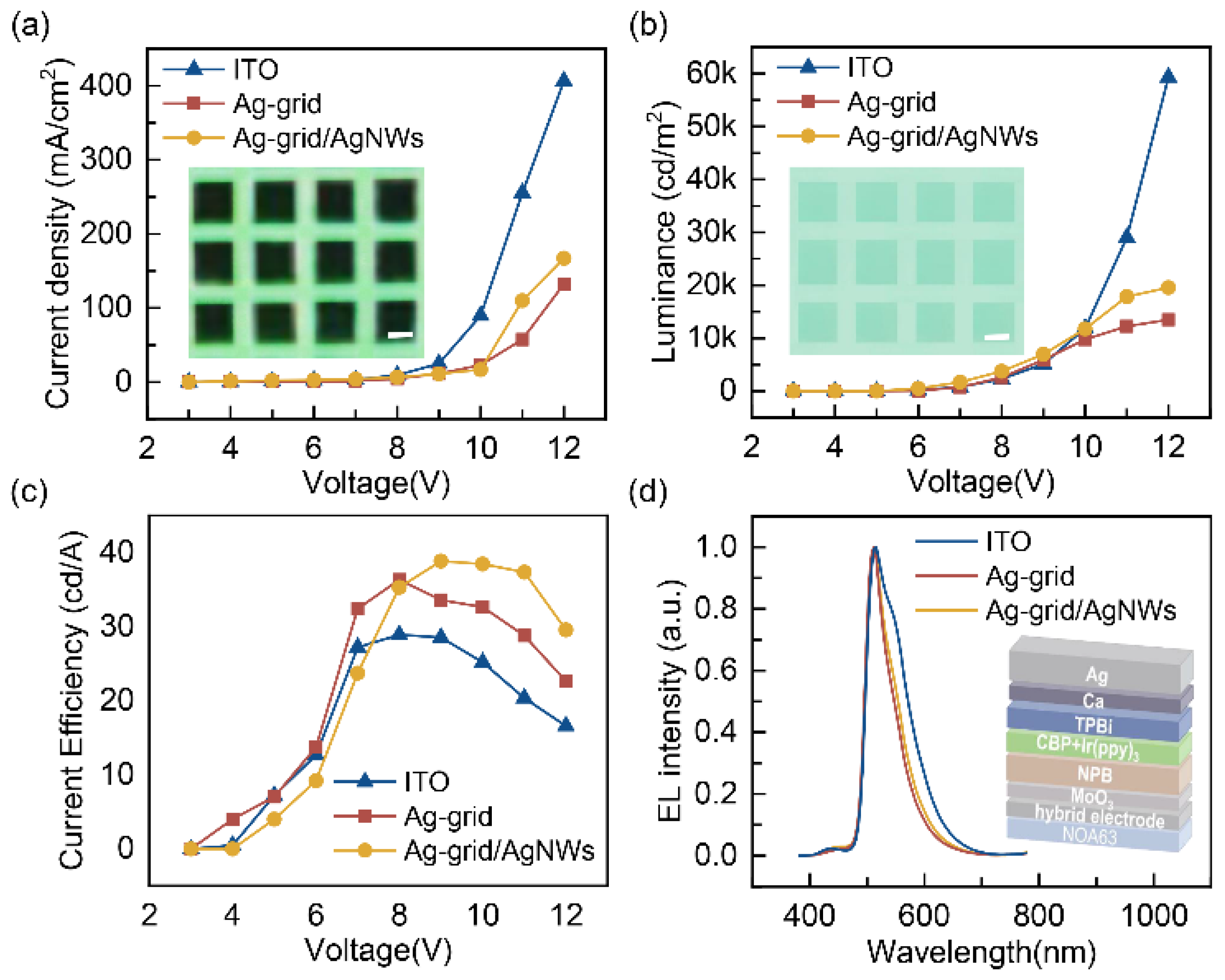
3. Results and Discussion

The surface topographies of the prepared Ag-grid and Ag-grid/AgNW hybrid film were described by scanning electron microscope (SEM), as shown in Figure 2a,b. The Ag-grid film fabricated by lithography and the etching process exhibited excellent long-range uniformity with clear boundaries, and the grid parameters were 15 μm in the line width and 30 μm in the gap width, which were well copied from the photomasks. In addition, there was no residual photoresist on the smooth surface of the Ag-grid, which could benefit its application in thin-film photoelectric devices. After bar-coating AgNWs on the top surface of the grid film, as shown in Figure 2b, an improved uniform conductivity could be expected, with additional charge transport channels formed in the non-conductive gaps in the Ag-grid.
To evaluate the feasibility of using the Ag-grid/AgNW hybrid film as a transparent electrode, the optical transmittance in the visible wavelength region and the electrical conductivity were measured and optimized by modifying the widths of the grid line and gap. As shown in Figure 2c, the Ag-grid film had high broadband transmittance, which was measured by a UV-Vis spectrophotometer (UV-2550, Shimadzu, Kyoto, Japan), and the transparency was improved by increasing the gap width and reducing the line width with enlarged optical windows. The optical performance of ITO was also compared. The Ag-grid/AgNW hybrid film showed a slightly lower transmittance because of the reflection and absorption of AgNWs. The optical transmittances at the wavelength of 550 nm of the samples with various grid parameters were compared, and the results are listed in Table 1. Photos of Ag-grid and Ag-grid/AgNW films prepared on NOA63 flexible substrate are the insets in Figure 2c,d, respectively, exhibiting good optical characteristics. The electrical performance of the Ag-grid and Ag-grid/AgNW films was measured by a four-point probe system (RTS-5, PROBES TECH, London, UK), and the sheet resistances (Rs) are also listed in Table 1. The variation in conductivity of the Ag-grid by changing the widths of the gap and line showed an opposite tendency to the optical transmittance, revealing the tradeoff between optical and electrical performance. The conductivities were further improved by the AgNWs in the hybrid film.
To balance and optimize the optoelectronic performance of the proposed Ag-grid/AgNW hybrid transparent and conductive film, figures of merit (FOMs) were calculated based on the Haacke Equation [22]:
F O M = T 10 R s
where T is the optical transmittance at a wavelength of 550 nm, and Rs are the sheet resistances of the corresponding samples. As listed in Table 1, the Ag-grid/AgNW hybrid film with a line width of 15 μm and a grid gap of 30 μm provided the best FOM value of 2.34 × 10⁻³/Ω, corresponding to the transmittance of 67.9% at 550 nm and the sheet resistance of 9 Ω/sq, which was chosen as the transparent electrode replacing the non-flexible ITO anode in flexible OLEDs.
The proposed Ag-grid/AgNW hybrid film had the desired optical transparency and electrical conductivity and was applied as the transparent anode in flexible OLEDs. The construction of these flexible devices is shown in the inset of Figure 3d. OLEDs based on the Ag-grid electrode, as well as the commercial ITO electrode on a flexible PET substrate (ITO/PET), were also prepared as a reference, and the EL characteristics of the flexible devices are summarized in Figure 3. The device with the Ag-grid electrode exhibited a netlike emission pattern with reduced effective light-emitting areas, as can be observed from the photo of the Ag-grid-based OLEDs in the inset of Figure 3a; this was caused by the non-uniform conductivity of the Ag-grid anode with large gaps between the conductive grid channels. By applying the Ag-grid/AgNW hybrid electrode as the replacement of the Ag-grid, an improved uniform light-emitting performance could be observed, as shown in the inset of Figure 3b, because the conductive channels of the Ag-grid were further connected by AgNWs. As a result, the maximum luminance of the flexible OLEDs was increased from 13,490 cd/m2 in the Ag-grid-based devices to 19,555 cd/m2 in the Ag-grid/AgNW-based devices. The ITO-based OLEDs showed the maximum luminance of 59,318 cd/m2, owing to the high transmittance and excellent uniform conductivity, with the largest effective emission area compared to the grid-based devices. On the other hand, OLEDs with Ag-grid/AgNW and Ag-grid anodes demonstrated the desired current efficiencies of 38.8 cd/A and 36.3 cd/A, respectively, which were significantly higher than those of the OLEDs based on the ITO electrode (28.9 cd/A). It should be noted that, in the calculation of current efficiency, the differences in the effective light-emitting areas between the ITO-based devices and grid-based devices can be eliminated. In spite of the higher transparency of ITO, as indicated in Figure 2, the OLEDs with the proposed Ag-grid/AgNW hybrid anode resulted in a 34% increase in efficiency compared to the ITO-based reference, which was guaranteed by the desired optoelectronic performance of the hybrid electrode and the suppressed power loss in the waveguide mode induced by ITO with a high refractive index [22,23]. Figure 3d shows the normalized EL spectra, and the slight differences in the spectra of the devices with different anodes were possibly induced by a weak microcavity mode [24].
A bending test was further applied to evaluate the flexibility and mechanical stability of the Ag-grid/AgNW hybrid electrode, as well as its application in flexible OLEDs. As shown in Figure 4a, the changes in the electrical conductivity of the electrodes after experiencing various bending cycles were recorded and compared by Rs/R0, where R0 referred to the original sheet resistance and Rs referred to the sheet resistance after the corresponding bending cycles. A commercial ITO/PET sample was also involved in this test as the reference. The Ag-grid/AgNW hybrid electrode exhibited perfect repetition and stable sheet resistance oscillations after 5000 bending cycles at a bending radius of 3 mm, demonstrating its promising durability in flexible applications. On the other hand, under the same bending conditions, the commercial ITO/PET showed a quick increase in conductivity from the original R0 of 9.2 Ω/sq to 276.3 Ω/sq, increasing by almost 30 times, owing to its brittleness with the quick formation of non-conductive cracks during the bending test. The flexible robustness of OLEDs based on the proposed Ag-grid/AgNW hybrid electrode and the ITO/PET electrode is compared in Figure 4b. Because of the poor mechanical stability of ITO, the devices’ performance noticeably decreased after only 100 bending instances with a bending radius of 3 mm. Instead, the flexible OLEDs with the proposed Ag-grid/AgNW hybrid electrode maintained 60% of their initial luminance after 1000 bending cycles, and the inset in Figure 4b shows the photo of the flexible OLEDs operated at 9 V under a bending condition, demonstrating their high flexibility and mechanical stability.

4. Conclusions

In summary, we proposed a flexible transparent conductive film based on an Ag-grid/AgNW hybrid construction, which demonstrated a good optical transparency of 67.9% at 550 nm, a high conductivity, with Rs = 9 Ω/sq, and excellent flexible stability, with constant electrical performance after 5000 bending cycles. The optical and electrical characteristics of the Ag-grid/AgNW hybrid film could be easily tuned by modifying the grid parameters. By applying the proposed hybrid conductive film as the transparent anode in flexible OLEDs to replace ITO or Ag-grid electrodes, uniform light emission was achieved, with improved EL performance. Compared to the flexible OLEDs based on the commercial ITO/PET electrode, the devices based on the proposed hybrid electrode exhibited not only the desired current efficiency, with a 34% increase, but also high flexibility and mechanical stability, revealing the potential applications of the proposed Ag-grid/AgNW hybrid film in flexible, stretchable, and wearable equipment.

Author Contributions

Conceptualization, J.F. and Y.B.; methodology, S.W. and H.Y.; writing—original draft preparation, H.W. and C.W.; writing—review and editing, G.Y. All authors have read and agreed to the published version of the manuscript.

Funding

This work was supported by the National Key Research and Development Program of China (2022YFB3607500), the National Natural Science Foundation of China (62374072, 62474079, 62274076, 62474082), the Science and Technology Development Program of Jilin (20220101109JC), and the Natural Science Foundation of Chongqing Municipality (CSTB2022NSCQ-MSX1155).

Institutional Review Board Statement

Not applicable.

Informed Consent Statement

Not applicable.

Data Availability Statement

Data underlying the results presented in this paper are not publicly available at this time but may be obtained from the authors upon reasonable request.

Conflicts of Interest

The authors declare that they have no conflicts of interest.

References

  1. Sannicolo, T.; Lagrange, M.; Cabos, A.; Celle, C.; Simonato, J.P.; Bellet, D. Metallic Nanowire-Based Transparent Electrodes for Next Generation Flexible Devices: A Review. Small 2016, 12, 6052–6075. [Google Scholar] [CrossRef] [PubMed]
  2. Sun, Y.; Chang, M.; Meng, L.; Wan, X.; Gao, H.; Zhang, Y.; Zhao, K.; Sun, Z.; Li, C.; Liu, S.; et al. Flexible organic photovoltaics based on water-processed silver nanowire electrodes. Nat. Electron. 2019, 2, 513–520. [Google Scholar] [CrossRef]
  3. Liu, Q.; Liu, Z.; Li, C.; Xie, K.; Zhu, P.; Shao, B.; Zhang, J.; Yang, J.; Zhang, J.; Wang, Q.; et al. Highly Transparent and Flexible Iontronic Pressure Sensors Based on an Opaque to Transparent Transition. Adv. Sci. 2020, 7, 2000348. [Google Scholar] [CrossRef] [PubMed]
  4. Helander, M.G.; Wang, Z.B.; Qiu, J.; Greiner, M.T.; Puzzo, D.P.; Liu, Z.W.; Lu, Z.H. Chlorinated Indium Tin Oxide Electrodes with High Work Function for Organic Device Compatibility. Science 2011, 332, 944–947. [Google Scholar] [CrossRef] [PubMed]
  5. Azani, M.-R.; Hassanpour, A.; Torres, T. Benefits, Problems, and Solutions of Silver Nanowire Transparent Conductive Electrodes in Indium Tin Oxide (ITO)-Free Flexible Solar Cells. Adv. Energy Mater. 2020, 10, 2002536. [Google Scholar] [CrossRef]
  6. Kwon, O.E.; Shin, J.W.; Oh, H.; Kang, C.M.; Cho, H.; Kwon, B.H.; Byun, C.W.; Yang, J.H.; Lee, K.M.; Han, J.H.; et al. A prototype active-matrix OLED using graphene anode for flexible display application. J. Inf. Disp. 2020, 21, 49–56. [Google Scholar] [CrossRef]
  7. Hao, T.; Ji, H.; Xu, D.; Liu, D.; Ren, Z.; Liu, W.; Zhang, Y.; Sun, J.; Zhao, J.; Zhang, L.; et al. Capillary Force-Induced Graphene Spontaneous Transfer and Encapsulation of Silver Nanowires for Highly-Stable Transparent Electrodes. ACS Appl. Mater. Interfaces 2024, 16, 40199–40209. [Google Scholar] [CrossRef]
  8. Snarski, L.; Biran, I.; Bendikov, T.; Pinkas, I.; Iron, M.A.; Kaplan-Ashiri, I.; Weissman, H.; Rybtchinski, B. Highly Conductive Robust Carbon Nanotube Networks for Strong Buckypapers and Transparent Electrodes. Adv. Funct. Mater. 2024, 34, 2309742. [Google Scholar] [CrossRef]
  9. Suh, B.L.; Kang, G.; Yoon, S.M.; Cho, S.; Moon, M.-W.; Sung, Y.-M.; Kim, M.-S.; Hur, K. Dimensional Control of Highly Anisotropic and Transparent Conductive Coordination Polymers for Solution-Processable Large-Scale 2D Sheets. Adv. Mater. 2023, 35, 2206980. [Google Scholar] [CrossRef]
  10. Tseng, C.-P.; Liu, F.; Zhang, X.; Huang, P.-C.; Campbell, I.; Li, Y.; Atkinson, J.T.; Terlier, T.; Ajo-Franklin, C.M.; Silberg, J.J.; et al. Solution-Deposited and Patternable Conductive Polymer Thin-Film Electrodes for Microbial Bioelectronics. Adv. Mater. 2022, 34, 2109442. [Google Scholar] [CrossRef]
  11. Kang, H.; Jung, S.; Jeong, S.; Kim, G.; Lee, K. Polymer-metal hybrid transparent electrodes for flexible electronics. Nat. Commun. 2015, 6, 6503. [Google Scholar] [CrossRef]
  12. Lu, Y.; Chen, M.; Jiang, L.; Cao, J.-j.; Li, H.; Lee, S.C.; Huang, Y. Oxygen vacancy engineering of photocatalytic nanomaterials for enrichment, activation, and efficient removal of nitrogen oxides with high selectivity: A review. Environ. Chem. Lett. 2022, 20, 3905–3925. [Google Scholar] [CrossRef]
  13. Hu, H.; Wang, S.; Wang, S.; Liu, G.; Cao, T.; Long, Y. Aligned Silver Nanowires Enabled Highly Stretchable and Transparent Electrodes with Unusual Conductive Property. Adv. Funct. Mater. 2019, 29, 1902922. [Google Scholar] [CrossRef]
  14. Atkinson, J.; Goldthorpe, I.A. Near-infrared properties of silver nanowire networks. Nanotechnology 2020, 31, 365201. [Google Scholar] [CrossRef] [PubMed]
  15. Chen, Z.; Yang, S.; Huang, J.; Gu, Y.; Huang, W.; Liu, S.; Lin, Z.; Zeng, Z.; Hu, Y.; Chen, Z.; et al. Flexible, Transparent and Conductive Metal Mesh Films with Ultra-High FoM for Stretchable Heating and Electromagnetic Interference Shielding. Nano-Micro Lett. 2024, 16, 92. [Google Scholar] [CrossRef] [PubMed]
  16. Kamijo, T.; de Winter, S.; Panditha, P.; Meulenkamp, E. Printed Copper Grid Transparent Conducting Electrodes for Organic Light-Emitting Diodes. ACS Appl. Electron. Mater. 2022, 4, 698–706. [Google Scholar] [CrossRef]
  17. Li, L.; Zhang, B.; Zou, B.; Xie, R.; Zhang, T.; Li, S.; Zheng, B.; Wu, J.; Weng, J.; Zhang, W.; et al. Fabrication of Flexible Transparent Electrode with Enhanced Conductivity from Hierarchical Metal Grids. ACS Appl. Mater. Interfaces 2017, 9, 39110–39115. [Google Scholar] [CrossRef]
  18. Feng, Y.; Song, J.; Han, G.; Zhou, B.; Liu, C.; Shen, C. Transparent and Stretchable Electromagnetic Interference Shielding Film with Fence-like Aligned Silver Nanowire Conductive Network. Small Methods 2023, 7, 2201490. [Google Scholar] [CrossRef]
  19. Qiao, J.; Huang, J.; Zhao, L.; Yuan, D.; Wang, P.; Xu, S. Line-Shaped Laser Lithography for Efficiently Fabricating Flexible Transparent Electrodes with Hierarchical Metal Grids across λ/10 to Microscale. Adv. Mater. Technol. 2023, 8, 2201209. [Google Scholar] [CrossRef]
  20. Yi, F.S.; Bi, Y.G.; Zhang, X.L.; Yin, D.; Liu, Y.F.; Feng, J.; Sun, H.B. Highly Flexible and Mechanically Robust Ultrathin Au Grid as Electrodes for Flexible Organic Light-Emitting Devices. IEEE Trans. Nanotechnol. 2019, 18, 776–780. [Google Scholar] [CrossRef]
  21. Cho, E.C.; Xie, J.; Wurm, P.A.; Xia, Y. Understanding the Role of Surface Charges in Cellular Adsorption versus Internalization by Selectively Removing Gold Nanoparticles on the Cell Surface with a I2/KI Etchant. Nano Lett. 2009, 9, 1080–1084. [Google Scholar] [CrossRef] [PubMed]
  22. Haacke, G. New figure of merit for transparent conductors. J. Appl. Phys. 1976, 47, 4086–4089. [Google Scholar] [CrossRef]
  23. Bi, Y.G.; Yi, F.S.; Ji, J.H.; Ma, C.; Wang, W.Q.; Feng, J.; Sun, H.B. Ultrathin Au Electrodes Based on a Hybrid Nucleation Layer for Flexible Organic Light-Emitting Devices. IEEE Trans. Nanotechnol. 2018, 17, 1077–1081. [Google Scholar] [CrossRef]
  24. Wang, M.; Lin, J.; Hsiao, Y.-C.; Liu, X.; Hu, B. Investigating underlying mechanism in spectral narrowing phenomenon induced by microcavity in organic light emitting diodes. Nat. Commun. 2019, 10, 1614. [Google Scholar] [CrossRef] [PubMed]
Figure 1. Schematic of the fabrication process of Ag-grid/AgNW hybrid transparent film, as well as flexible OLEDs with Ag-grid/AgNW anodes: (a) deposition of Ag film on Si substrate; (b) photoresist S-1805 was spin-coated on Ag film; (c) lithographic exposure with grid mask; (d) wet-etching Ag film to obtain Ag-grid film; (e) bar-coating AgNW suspension; (f) pattern the Ag-grid/AgNW film with adhesive tape; (g) NOA63 spin-coated and cured by UV exposure; (h) cured NOA63 with Ag-grid/AgNW film was peeled off; and (i) flexible OLEDs were deposited.
Photonics 12 00272 g001
Figure 2. SEM images and zoomed-in SEM images of (a) Ag-grid film and (b) Ag-grid/AgNW film. Transmittance spectra of (c) Ag-grid films and (d) Ag-grid/AgNW films with various grid parameter. The insets in (c,d) refer to the photos of Ag-grid and Ag-grid/AgNW films with a line width of 15 μm and a grid gap of 30 μm on NOA63 flexible substrate, respectively.
Photonics 12 00272 g002
Figure 3. EL performance of the flexible OLEDs: (a) current density–voltage, (b) luminance–voltage, (c) current efficiency–voltage, and (d) normalized EL spectra of OLEDs based on the ITO, Ag-grid, and Ag-grid/AgNW anode, respectively. The insets in (a) and (b) refer to the photos of OLEDs with Ag-grid and Ag-grid/AgNW anodes, respectively. The devices were operated by 9 V, and the photos were captured by an optical microscope. The scale bar in the photos is 20 μm. The inset in (d) shows the schematic structure of flexible OLEDs.
Photonics 12 00272 g003
Figure 4. Flexibility and mechanical stability of the flexible electrodes and flexible OLEDs: (a) changes in sheet resistance of Ag-grid/AgNW and ITO electrode as a function of the bending cycles, where R0 and Rs refer to the sheet resistance before and after bending, respectively, and the thickness of the Ag-grid is 18 nm; and (b) normalized luminance of the OLEDs operated at 9 V as a function of the bending cycles. The inset in (b) shows the photograph of the flexible OLEDs operated at 9 V after bending.
Photonics 12 00272 g004
Table 1. Optical and electrical performance of Ag-grid and Ag-grid/AgNW films.
Line Width–Gap WidthT (%)Rs (Ω/sq)FOM (×10−3/Ω)
15 μm–30 μm a70.7714.062.24
15 μm–40 μm a71.6622.191.61
15 μm–50 μm a73.4238.041.19
15 μm–60 μm a74.6643.111.24
15 μm–70 μm a78.5167.041.32
10 μm–50 μm a78.9946.202.04
10 μm–60 μm a79.5756.171.81
15 μm–30 μm b67.999.002.34
15 μm–40 μm b68.9215.011.61
15 μm–50 μm b69.0116.211.51
15 μm–60 μm b72.1817.142.23
15 μm–70 μm b72.4924.181.65
10 μm–50 μm b73.2919.882.24
10 μm–60 μm b74.0622.152.24
a refers to the Ag-grid samples, while b refers to the Ag-grid/AgNW samples.
Disclaimer/Publisher’s Note: The statements, opinions and data contained in all publications are solely those of the individual author(s) and contributor(s) and not of MDPI and/or the editor(s). MDPI and/or the editor(s) disclaim responsibility for any injury to people or property resulting from any ideas, methods, instructions or products referred to in the content.

