Study of a Graphene Surface Plasmon Polariton-Based Dielectric Laser Accelerator

 ,
,
Abstract
:1. Introduction
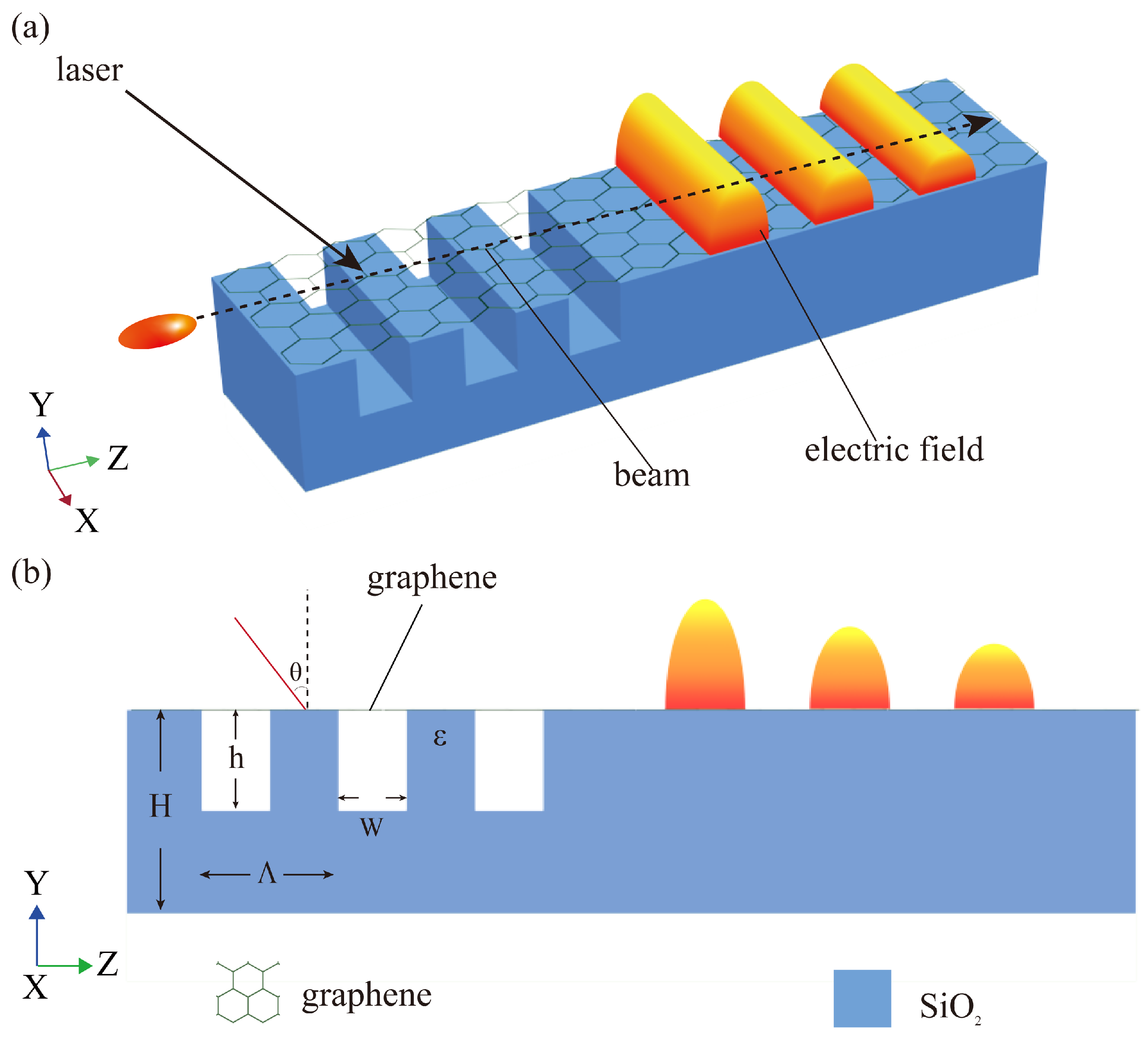
2. Principle
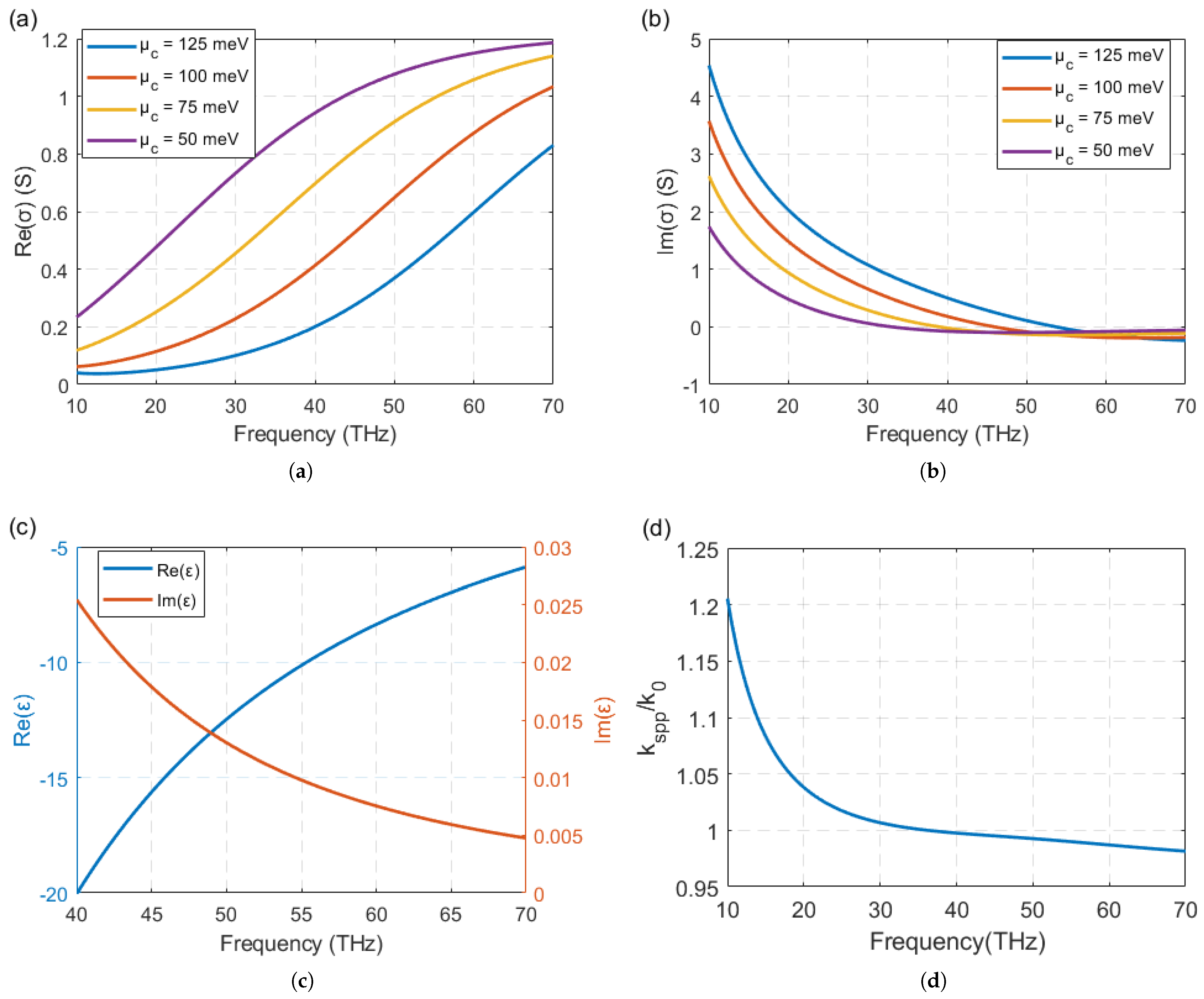
2.1. Graphene Conductivity and Grating Structure
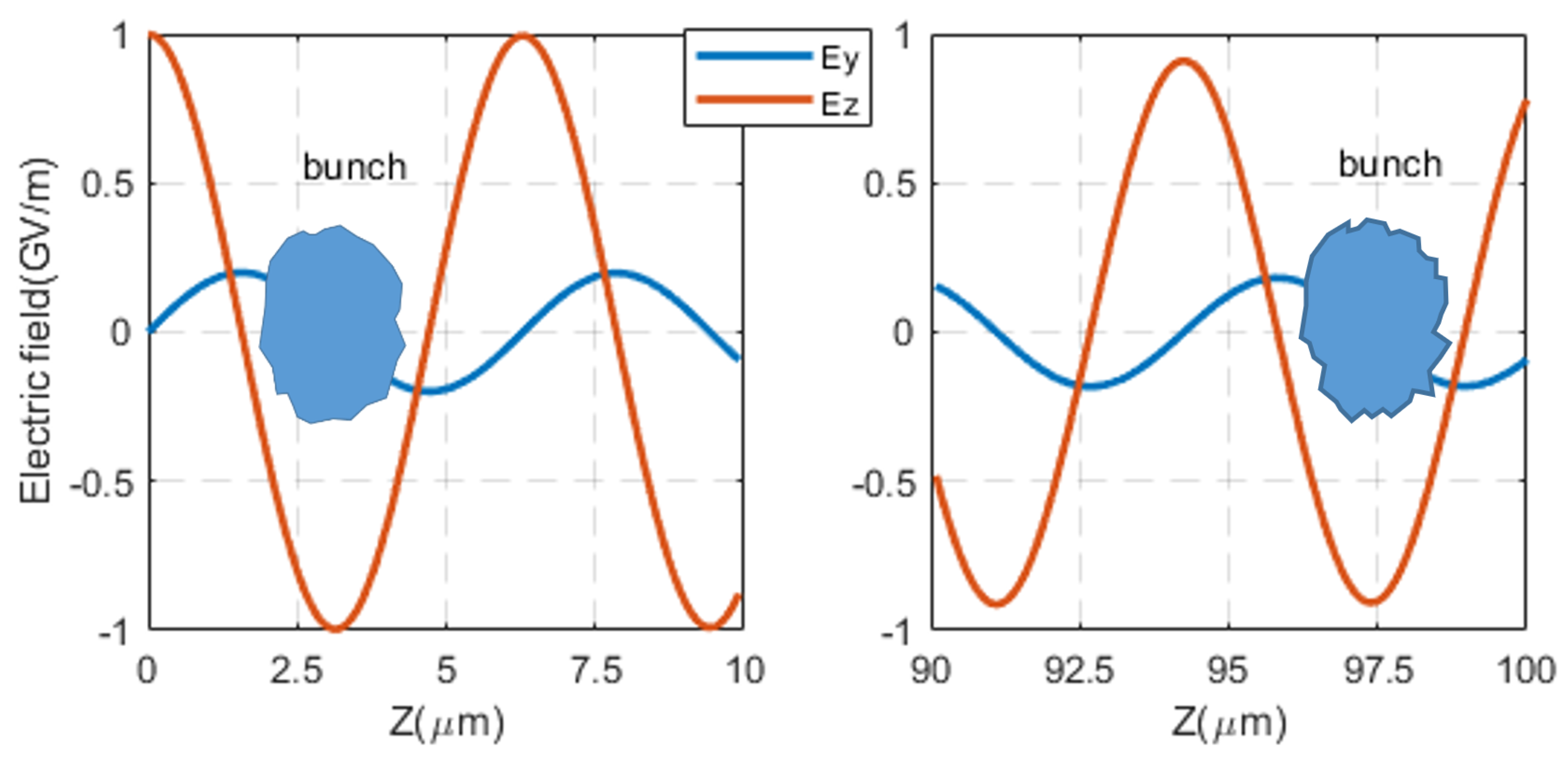
2.2. Interaction Length
3. FDTD Simulation
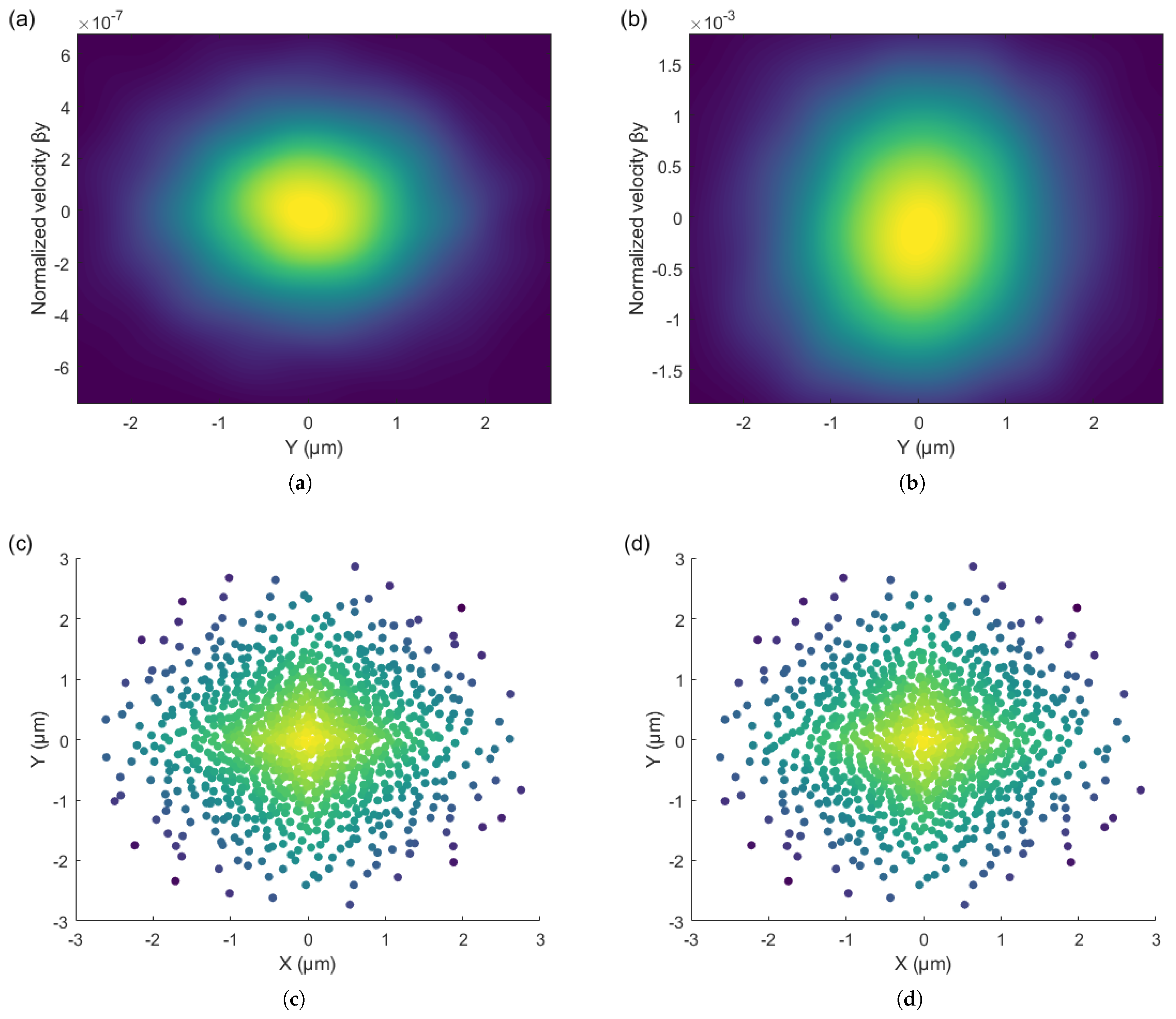
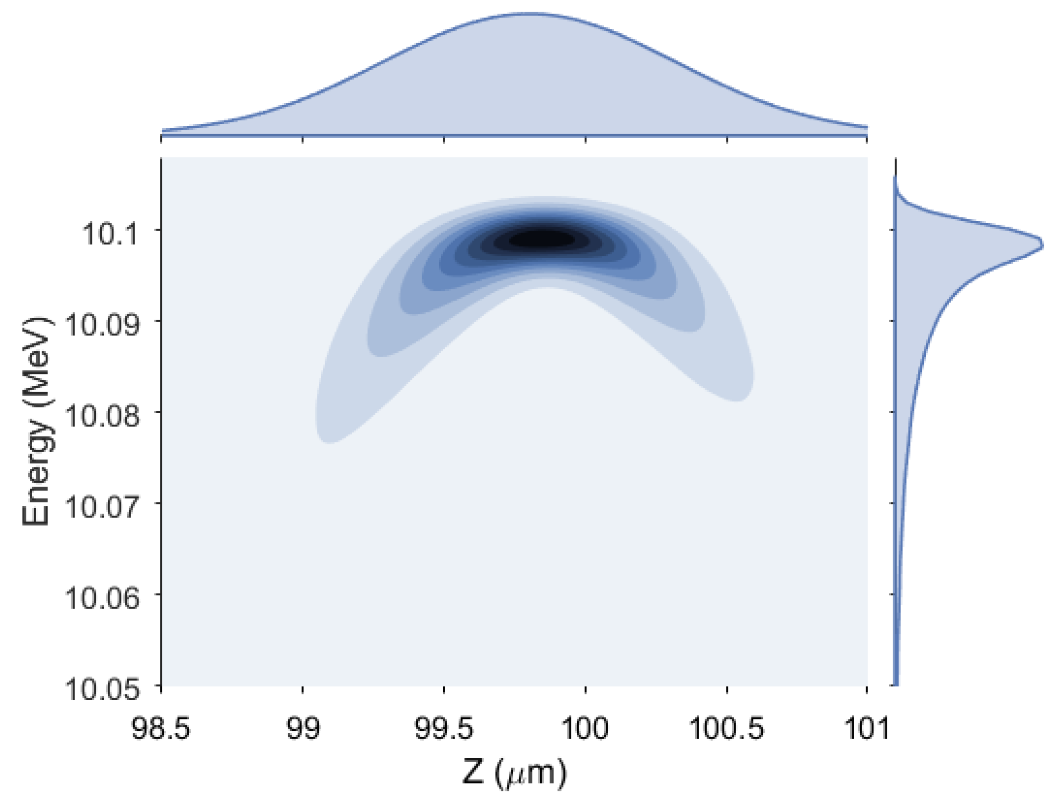
4. Theoretical Calculations of the Surface Electric Field and Particle Tracking
5. Discussion
6. Conclusions
Author Contributions
Funding
Institutional Review Board Statement
Informed Consent Statement
Data Availability Statement
Conflicts of Interest
References
- Wootton, K.P.; McNeur, J.; Leedle, K.J. Dielectric Laser Accelerators: Designs, Experiments, and Applications. Rev. Accel. Sci. Technol. 2016, 9, 105–126. [Google Scholar] [CrossRef]
- Litos, M.; Adli, E.; An, W.; Clarke, C.; Clayton, C.E.; Corde, S.; Delahaye, J.P.; Engl, R.J.; Fisher, A.S.; Frederico, J.; et al. High-efficiency acceleration of an electron beam in a plasma wakefield accelerator. Nature 2014, 515, 92–95. [Google Scholar] [CrossRef] [PubMed]
- Joshi, C.; Malka, V. Focus on laser-and beam-driven plasma accelerators. New J. Phys. 2010, 12, 045003. [Google Scholar] [CrossRef]
- Teryaev, V.E. Two-stage multi-beam linear accelerator EVT. Nucl. Instruments Methods Phys. Res. Sect. A Accel. Spectrometers Detect. Assoc. Equip. 2018, 909, 332–335. [Google Scholar] [CrossRef]
- England, R.J.; Noble, R.J.; Bane, K.; Dowell, D.H.; Ng, C.K.; Spencer, J.E.; Tantawi, S.; Wu, Z. Dielectric laser accelerators. Rev. Mod. Phys. 2014, 86, 1337–1389. [Google Scholar] [CrossRef]
- Wei, Y.; Ibison, M.; Resta-Lopez, J.; Welsch, C.P.; Ischebeck, R.; Jamison, S.; Xia, G.; Dehler, M.; Prat, E.; Smith, J.D.A. Energy efficiency studies for dual-grating dielectric laser-driven accelerators. Nucl. Instruments Methods Phys. Res. Sect. A Accel. Spectrometers Detect. Assoc. Equip. 2018, 909, 257–260. [Google Scholar]
- Leedle, K.J.; Ceballos, A.; Deng, H.; Solgaard, O.; Pease, R.F.; Byer, R.L.; Harris, J.S. Dielectric laser acceleration of sub-100 keV electrons with silicon dual-pillar grating structures. Opt. Lett. 2015, 40, 4344–4347. [Google Scholar]
- Breuer, J.; Hommelhoff, P. Laser-Based Acceleration of Nonrelativistic Electrons at a Dielectric Structure. Phys. Rev. Lett. 2013, 111, 134803. [Google Scholar] [CrossRef]
- Broaddus, P.; Egenolf, T.; Black, D.S.; Murillo, M.; Woodahl, C.; Miao, Y.; Murillo, M.; Woodahl, C.; Miao, Y.; Niedermayer, U.; et al. Subrelativistic Alternating Phase Focusing Dielectric Laser Accelerators. Phys. Rev. Lett. 2024, 132, 085001. [Google Scholar] [CrossRef]
- Maier, S.A. Plasmonics: Fundamentals and Applications; Springer: New York, NY, USA, 2007; Volume 1. [Google Scholar]
- Ajimo, J.J. Study of Surface Plasmon Polariton propagation, interference and diffraction using Plasmon Tomography. Ph.D. Thesis, Texas Tech University, Lubbock, TX, USA, 2011. [Google Scholar]
- Jablan, M.; Buljan, H.; Soljačić, M. Plasmonics in graphene at infrared frequencies. Phys. Rev. B 2009, 80, 245435. [Google Scholar] [CrossRef]
- Lu, H.; Zeng, C.; Zhang, Q.; Liu, X.; Hossain, M.M.; Reineck, P.; Gu, M. Graphene-based active slow surface plasmon polaritons. Sci. Rep. 2015, 5, 8443. [Google Scholar] [CrossRef]
- Fu, J.; Lv, B.; Li, R.; Ma, R.; Chen, W.; Wang, Z. Excitation of surface plasmon polaritons in an inhomogeneous graphene-covered grating. Plasmonics 2017, 12, 209–213. [Google Scholar]
- Lin, I.T.; Fan, C.; Liu, J.M. Propagating and localized graphene surface plasmon polaritons on a grating structure. IEEE J. Sel. Top. Quantum Electron. 2016, 23, 144–147. [Google Scholar] [CrossRef]
- Nicholls, D.P.; Oh, S.H. Launching graphene surface plasmon waves with vanishingly small periodic grating structures. JOSA A 2021, 38, 556–563. [Google Scholar]
- Xiao, S.; Zhu, X.; Li, B.H.; Mortensen, N.A. Graphene-plasmon polaritons: From fundamental properties to potential applications. Front. Phys. 2016, 11, 117801. [Google Scholar] [CrossRef]
- Falkovsky, L.A. Optical properties of graphene. J. Phys. Conf. Ser. 2008, 129, 012004. [Google Scholar] [CrossRef]
- Gusynin, V.; Sharapov, S.; Carbotte, J. Sum rules for the optical and Hall conductivity in graphene. Phys. Rev. B 2007, 75, 165407. [Google Scholar]
- Hanson, G.W. Dyadic Green’s functions and guided surface waves for a surface conductivity model of graphene. J. Appl. Phys. 2008, 103, 064302. [Google Scholar]
- Vakil, A. Transformation Optics Using Graphene: One-Atom-Thick Optical Devices Based on Graphene; University of Pennsylvania: Philadelphia, PA, USA, 2012. [Google Scholar]
- Zhang, J.; Zhang, L.; Xu, W. Surface plasmon polaritons: Physics and applications. J. Phys. D Appl. Phys. 2012, 45, 113001. [Google Scholar]
- Jeschke, H.O.; Garcia, M.E.; Bennemann, K.H. Theory for the Ultrafast Ablation of Graphite Films. Phys. Rev. Lett. 2001, 87, 015003. [Google Scholar]
- Roberts, A.; Cormode, D.; Reynolds, C.; Newhouse-Illige, T.; LeRoy, B.J.; Sandhu, A.S. Response of graphene to femtosecond high-intensity laser irradiation. Appl. Phys. Lett. 2011, 99, 051912. [Google Scholar]
- Sun, L.; Liu, W.; Zhou, J.; Zhu, Y.; Yu, Z.; Liu, Y.; Jia, Q.; Sun, B.; Xu, H. GV/m on-chip particle accelerator driven by few-cycle femtosecond laser pulse. New J. Phys. 2021, 23, 063031. [Google Scholar]
- Bar-Lev, D.; Scheuer, J. Plasmonic metasurface for efficient ultrashort pulse laser-driven particle acceleration. Phys. Rev. Spec. Top.-Accel. Beams 2014, 17, 121302. [Google Scholar]
- Sapra, N.V.; Yang, K.Y.; Vercruysse, D.; Leedle, K.J.; Black, D.S.; England, R.J.; Su, L.; Trivedi, R.; Miao, Y.; Solgaard, O.; et al. On-chip integrated laser-driven particle accelerator. Science 2020, 367, 79–83. [Google Scholar]
- Chlouba, T.; Shiloh, R.; Kraus, S.; Brückner, L.; Litzel, J.; Hommelhoff, P. Coherent nanophotonic electron accelerator. Nature 2023, 622, 476–480. [Google Scholar] [CrossRef]
- Zheng, D.; Huang, S.; Li, J.; Tian, Y.; Zhang, Y.; Li, Z.; Tian, H.; Yang, H.; Li, J. Efficiently accelerated free electrons by metallic laser accelerator. Nat. Commun. 2023, 14, 5857. [Google Scholar]
- Brückner, L.; Chlouba, T.; Morimoto, Y.; Schönenberger, N.; Shibuya, T.; Siefke, T.; Zeitner, U.D.; Hommelhoff, P. Mid-infrared dielectric laser acceleration in a silicon dual pillar structure. Opt. Express 2024, 32, 28348–28355. [Google Scholar]
- Zhang, L.; Liu, W.; Jia, Q.; Xu, H.; Lu, Y. Inverse-Cherenkov Dielectric Laser Accelerator With a Prism-Slab Structure Driven by Single-Side Laser. IEEE Trans. Electron Devices 2023, 70, 3308–3314. [Google Scholar]
- Liu, W.; Zhang, L.; Liu, Y.; Jia, Q.; Sun, B.; Xu, H. Toward a Laser-Driven Traveling-Wave Linac on a Chip. Phys. Rev. Appl. 2023, 19, 044066. [Google Scholar]


| Parameter | Value | Note |
|---|---|---|
| W | 3.205 m | 1/2 grating constant |
| 6.41 m | Grating constant | |
| H | 5.705 m | Base thickness + h |
| h | 3.205 m | Grating tooth height |
| 21 deg | Angle of incidence | |
| n | 2.5 m | Reflective index |
| 100 meV | Chemical potential | |
| f | 53.375 THz | Laser frequency |
Disclaimer/Publisher’s Note: The statements, opinions and data contained in all publications are solely those of the individual author(s) and contributor(s) and not of MDPI and/or the editor(s). MDPI and/or the editor(s) disclaim responsibility for any injury to people or property resulting from any ideas, methods, instructions or products referred to in the content. |
© 2025 by the authors. Licensee MDPI, Basel, Switzerland. This article is an open access article distributed under the terms and conditions of the Creative Commons Attribution (CC BY) license (https://creativecommons.org/licenses/by/4.0/).
Share and Cite
Lin, H.; Liao, T.; Wei, X.; Wang, W.; Du, J.; Zhi, Y. Study of a Graphene Surface Plasmon Polariton-Based Dielectric Laser Accelerator. Photonics 2025, 12, 292. https://doi.org/10.3390/photonics12040292
Lin H, Liao T, Wei X, Wang W, Du J, Zhi Y. Study of a Graphene Surface Plasmon Polariton-Based Dielectric Laser Accelerator. Photonics. 2025; 12(4):292. https://doi.org/10.3390/photonics12040292
Chicago/Turabian StyleLin, Hongxiang, Tianfa Liao, Xiaohui Wei, Wenyuan Wang, Juan Du, and Yaoxuan Zhi. 2025. "Study of a Graphene Surface Plasmon Polariton-Based Dielectric Laser Accelerator" Photonics 12, no. 4: 292. https://doi.org/10.3390/photonics12040292
APA StyleLin, H., Liao, T., Wei, X., Wang, W., Du, J., & Zhi, Y. (2025). Study of a Graphene Surface Plasmon Polariton-Based Dielectric Laser Accelerator. Photonics, 12(4), 292. https://doi.org/10.3390/photonics12040292