1. Introduction
With the rapid development of solar photovoltaic (PV) technology, solar energy as a clean and sustainable type of renewable energy has become one of the important energy sources to replace traditional fossil fuels. Countries all over the world have been vigorously developing the PV industry [
1]. At present, the mainstream solar cells mainly include monocrystalline silicon (MC-Si) and polycrystalline silicon (PC-Si) cells, which have certain advantages and disadvantages. MC-Si cells have high monochromatic incident photon-to-electron conversion efficiency (IPCE), but their service life is short and manufacturing cost is high. In contrast, PC-Si cells have a long service life and low manufacturing cost but their IPCE is low. In recent years, mono-like cast silicon (MLC-Si) solar cells have attracted great attention because of their advantages, such as high IPCE and low manufacturing cost, and have become highly popular in the PV market [
2,
3].
As in the production of MC-Si and PC-Si cells, various types of defects, such as breakage, scratches, dirt, and dislocation, will inevitably occur in the production process of MLC-Si cells due to a range of unstable factors, including mechanical stress, thermal stress, and human error. Although the MLC-Si wafers have fewer defects compared with the conventional PC-Si wafers, the probability of certain defects, such as dislocation, is still high because of the characteristics of the casting method, and the feature detection of MLC-Si wafers is complex. Compared to the defects created in the processing stage, dislocation has the following characteristics. First, dislocation is a type of crystal defect occurring in the form of a line. As it cannot be eliminated in subsequent processing, it will always exist inside the silicon wafer. Second, unlike external defects, such as breakage, edge collapse, and dirt, dislocation affects the PV cells in an indirect way. Namely, dislocations will become the Shockley–Read–Hall recombination centers for the minority carriers inside the crystal, thus reducing the IPCE of the cell by shortening the life span of carriers [
4]. Third, the distribution of dislocations exhibits a certain pattern, namely, the edge silicon ingots have a higher dislocation density than those in the central zone. For a single silicon ingot, the head and tail parts have a higher dislocation density than the middle part.
At present, silicon wafer manufacturers generally classify silicon wafers using the minority carrier lifetime [
5]. Although there are many methods for testing minority carrier lifetime, there has been a lack of internationally recognized standard sample chips, so there has been no concept of absolute accuracy in minority carrier lifetime testing. In addition, to assess the influence of dislocation on the silicon wafer quality using the conventional machine vision technology, it is needed to extract the defect region using an image processing algorithm and then to perform formula fitting according to the characteristic variables, such as area and shape. However, there are some difficulties in this process. First, extracting the defect features using traditional image processing methods based on the machine vision missed rate and false detection rate has the drawback of high missed and false detection rates, which affects the accuracy of subsequent formula fitting. Second, defect distribution is not fixed and defects’ locations are random, which introduces great challenges in the subsequent work.
2. Related Research
With the development of science and technology, non-contact image acquisition of silicon wafers has been realized using photoluminescence technology [
6,
7,
8], and many studies on defect extraction from silicon wafer images using relevant deep learning algorithms have been conducted. Bartler et al. [
9] developed a deep learning model for detecting defective solar cells in a PV module based on the VGG-16 deep learning network model. They introduced a batch normalization layer to the network model to improve the model training speed, enabling the improved network model to detect defective solar cells in a PV module automatically. Qian et al. [
10] proposed a micro-crack detection method, which uses both short- and long-term deep features. The short-term deep features are learned from the input image by a stacked denoising autoencoder (SDAE), whereas the long-term deep features are learned from a large number of commonly seen images of natural scenes by a convolutional neural network. The combined usage of short- and long-term deep features enables effective detection of various micro-cracks. Zhang et al. [
11] proposed a solar cell surface defect detection method based on a model that fuses the Faster R-CNN and the R-FCN. They improved the detection accuracy through the complementary fusion of detection results of the Faster R-CNN and R-FCN models.
However, in the actual production process, only when dislocation defects reduce the IPCE of a battery cell to an unacceptable range for an enterprise will the battery cell be judged as a non-conforming product. The above-mentioned methods can only locate and extract defects, whereas judging whether a battery cell is conforming or non-conforming is beyond their scope of capabilities. The silicon wafer quality evaluation algorithm proposed in this paper simplifies this process so that it can predict the battery’s IPCE directly and then judge whether the product is conforming. The quality evaluation problem is essentially a regression problem, that is, to find the best fitting relationship between the input and output variables on the basis of processing a large amount of data and then predict new data. To solve this problem, different methods can be used. For instance, Mishra et al. [
12] proposed a PV power generation prediction model based on the wavelet transform and LSTM-dropout network. This model uses wavelet transform to preprocess data of temperature, visibility, and cloudiness and a deep learning network model to accomplish the PV power generation prediction. Zhong et al. [
13] proposed an improved convolutional neural network model for predicting the remaining service life of aircraft engines. This model performs convolutional operations in the time dimension to obtain the relationship between the data trend and the remaining service life of an aircraft engine, which is suitable for various high-dimensional data predictions.
Drawing upon the above-presented research methods in different fields and focusing on ML-Si wafers, this paper uses deep learning technology to evaluate the influence of dislocations quantitatively and realize quality prediction of silicon wafers.
3. Materials and Methods
3.1. Dataset Construction
3.1.1. Image Acquisition
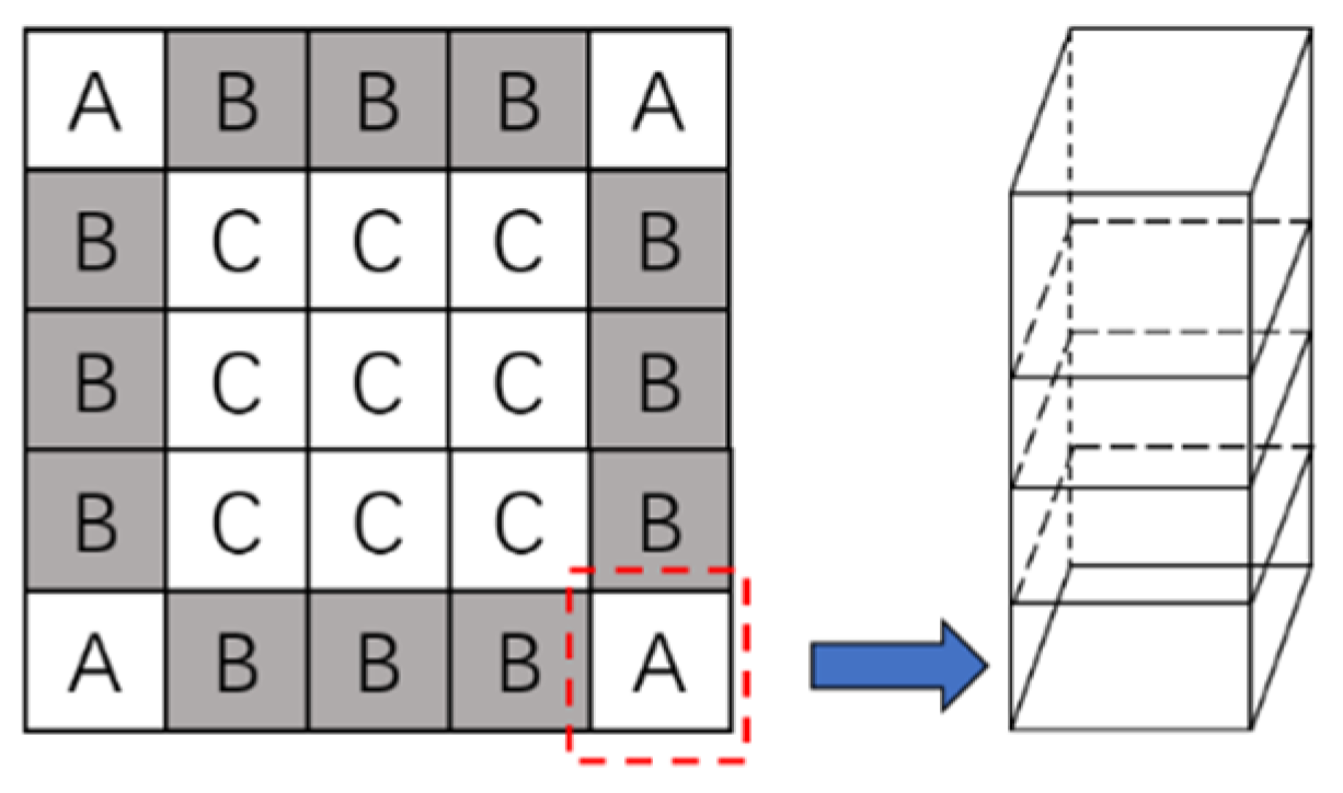
Since dislocations are distributed unevenly in a silicon ingot, it is necessary to formulate the right scheme for material selection. Specifically, the silicon ingot was divided into zones A, B, and C, corresponding to the corner, edge, and center, respectively, as shown in
Figure 1.
Sample wafers were taken from each zone of the silicon ingot. From bottom to top, three silicon wafers were taken at an interval of five wafers, obtaining a total of 1120 wafers. A number was inscribed on the upper-right corner of a silicon wafer by a laser, and then the image of the wafer was acquired by an image acquisition device.
3.1.2. Image Labeling
For solar silicon wafers, the IPCE represents an important indicator of product quality. Therefore, the IPCE value of each sample wafer was used as a label of that wafer. Specifically, the sample silicon wafers were made into battery cells and their IPCE values were obtained through testing. The following measures were taken to ensure data accuracy. The processes of sample production and testing were supervised to reduce the risk of mixing unmarked and marked battery cells in each stage, and the damaged samples were recorded in the production process. To reduce the influence of the production process on the results, the mean value of the IPCE values of three consecutive samples was calculated and used as the IPCE value of these three samples. If the number of remaining samples was less than two, the sample data would be discarded. After the above operation was completed, 1000 samples that could be used in the experiment were obtained. These samples and their corresponding IPCE values were compiled into a dataset.
3.1.3. Data Enhancement
Before convolutional neural network training, it is necessary to enhance data so as to prevent over-fitting due to the small number of datasets. Some commonly used data enhancement methods are random shear, mirror image, and rotation. It is worth noting that to study the relationship between dislocation and silicon wafer quality, it is necessary to ensure image integrity. However, random cutting and translation operations would compromise image integrity, so these operations could not be used for data enhancement. To ensure data amount after enhancement, certain image processing algorithms, as well as random image rotation and mirroring, were used in this study as image enhancement methods. Specifically, the frequency domain filtering operation adopted the line trance removal algorithm based on discrete Fourier transform and the spatial domain filtering operation was performed by an image denoising algorithm based on mean filtering, as shown in
Figure 2. After data enhancement, the total number of samples was 6000. The training and testing sets were formed by randomly selecting data from the dataset. The data volume ratio of the training set to the testing set was 4:1.
3.2. Deep Learning Model for Battery Quality Evaluation
3.2.1. VGG Network Model
The VGG network [
14] mainly improves the network performance by increasing the depth of the network, mainly by stacking multiple 3 × 3 convolutional kernels instead of large-scale convolutional kernels, which can reduce the required parameter number without shrinking the receptive field.
The main purpose of the traditional VGG network model is image classification. The problem of silicon wafer quality prediction studied in this paper is a regression problem. In a network structure, the regression layer is often used to solve the regression problem. This structure can predict the relationship between the input and output variables. In silicon wafer quality prediction, the input variable represents a feature extracted from the silicon wafer image by a convolutional neural network and the output variable is an IPCE value. Therefore, when constructing the VGG network structure, the Softmax layer is replaced with the regression layer. The adjusted VGG-16 network structure is presented in
Figure 3.
3.2.2. Resnet Network Model
The Resnet network [
15], also known as a residual network, has been mainly used to solve the problem of network performance degradation with the network layer number. During the backpropagation process, if a network is too deep, the gradient gradually diminishes when the error reaches the front end. As the network depth increases, the network performance degrades. Therefore, a residual element is introduced to connect the output of the previous layer directly to its subsequent layer so as to suppress the degradation. Resnet-18 in the Resnet network model is selected as a migration model to fine-tune the fully connected and classification layers of the network.
3.2.3. GoogleNet Network Model
The GoogleNet network [
16] improves the model quality by increasing the model width and introduces the inception structure [
17]. Unlike the VGG network, which obtains a high-accuracy model by increasing the model depth, when the number of network layers is too deep, the large number of parameters not only requires large memory and computing power but also brings the problems of gradient disappearance and gradient explosion. The Inception structure is composed of 1 × 1, 3 × 3, and 5 × 5 convolution kernels. By using the convolution kernels of different sizes to obtain different receptive fields and then performing information fusion, the GoogleNet network achieves good results in image feature extraction. To prevent over-fitting, the dropout structure [
18] is adopted in the network. The purpose of this arrangement is to randomly abandon some neurons so as to reduce the number of neurons participating in training, thus mitigating the over-fitting effect of the network. Meanwhile, the network uses the global mean pooling layer to replace the full connection layer, which greatly reduces the model parameters number. In this study, the prediction of silicon wafer quality is realized by fine-tuning the structure of the last fully connected layer of the network.
3.3. Model Evaluation Index
To test the accuracy and stability of the proposed model in experiments, the root mean square error (RMSE) was used as an evaluation index. The RSME indicates the deviation of the predicted value from the real value. It can better reflect the prediction errors of different models when the same dataset is used. The mathematical expression of the RSME is as follows:
where
and
refer to the predicted and real values of the
th piece of data, respectively.
3.4. Model Optimization Algorithm
The ADAM [
19] and SGDM [
20] optimization algorithms were chosen to optimize the VGG-16, VGG-19, Resnet-18, and GoogleNet network models and to find the best-performance model using the RMSE index. For the purpose of controlling the variables, the hyperparameters of all models were set to the same values: the initial learning rate was 0.00001; the maximum training iteration number was 50 epochs (periods); the learning rate increased by 0.1 times the previous value every 30 epochs; the number of training images in each iteration was 12; every 10 iterations, the verification was performed, and the RMSE and the verification loss were calculated.
4. Experimental Verification
4.1. Experimental Setup
The experimental system included the deep learning framework of Python 1.8.1, and the software was developed using Python 3.8 programming language. All experiments were carried out in the system environment of Windows 10. The key hardware components of the experiment system were the i5-9600kf CPU at 3.70 GHz and the NVIDIA RTX 2070 super 8G GPU.
4.2. Experimental Results Analysis
4.2.1. Optimizer Selection
Different optimization algorithms were used to train the network model to determine the impact of the optimization algorithm on the network model performance. As shown in
Figure 4, in the ML-Si wafer quality evaluation, the ADAM optimization algorithm yielded good performance in different networks. During the whole process of network iteration, the RMSE curve of the model using the ADAM optimization algorithm tended to be stable, while the error curve of the model using the SGDM optimization algorithm exhibited considerable fluctuations. In the stable state, the RMSE value of the model using the ADAM algorithm was always smaller than that of the model using the SGDM algorithm. These results indicate that the ADAM optimization algorithm has a better effect on the quality prediction model of ML-Si wafers than the SGDM algorithm. For this reason, the ADAM optimization algorithm was selected for the subsequent training.
4.2.2. Model Performance Comparison
Transfer learning was performed on the VGG-16, VGG-19, Resnet-18, and GoogleNet models. All the models were trained by the ADAM optimization algorithm, and the loss and RMSE curves of the models are shown in
Figure 5. After that, 100 images were randomly selected from the test set and the trained networks were used to make predictions of these images. The RMSE and reasoning speed values were calculated and recorded, as shown in
Table 1.
As shown in
Figure 5a, the training losses of the four network models were in the normal convergence state. During the training process, the losses of the VGG-16 and VGG-19 network models decreased with relatively large fluctuations, while the loss fluctuations of the GoogleNet and Resnet-18 models were small. As presented in
Figure 5b and
Table 1, the RMSE values of the four network models were similar. The RMSE value of Resnet-18 was the largest (0.80), which indicated that the performance of this model in predicting the quality of ML-Si wafers was not high. With an RMSE value of 0.333, the VGG-19 model achieved the best performance. Regarding the model training time, the GoogleNet model requires the longest training time (21.04 min), while the training time of the Resnet-18 model is the shortest (10.57 min). Although the VGG-19 model required a training time twice as long as that of the Resnet-18 model, the prediction performance of the former was 2.5 times higher than that of the latter. Regarding the model reasoning speed, the Resnet-18 model was the fastest, reaching the reasoning speed of 32.62 FPS. There was a slight difference in the reasoning speed between the VGG and GoogleNet models. In summary, the VGG-19 network achieved the best overall performance, with an RMSE value of 0.33 and a reasoning speed of 14.45 FPS.
4.3. VGG-19 Network Improvement
To improve the prediction accuracy further, the crowd counting problem was considered. In the problem of crowd counting, accurate counting could be difficult to achieve due to various factors, including mutual occlusion between individuals caused by congestion, high similarity between people and background, and difficult features extraction from the high-resolution background. At present, an effective way to solve this type of problem is to use the method of predicted density map. Ranjan [
21] proposed iterative counting convolutional neural networks (ic-CNN) with a two-branch structure, where the first branch generates a low-resolution density map and the second branch incorporates the low-resolution prediction and feature maps from the first branch to generate a high-resolution density map. Jiang [
22] proposed an approach to alleviate the counting performance differences in different regions, which consists of the density attention network (DANet) and the attention scaling network (ASNet). DANet provides ASNet with attention masks related to regions of different density levels. ASNet first generates density maps and scaling factors and then multiplies them by attention masks to output separate attention-based density maps. These density maps are summed to give the final density map.
With regard to the problem of detecting defects in silicon wafers, it is discovered that dislocations in a silicon wafer obey a certain distribution; namely, the dislocation density at the edge of a silicon ingot is higher than that in the middle. This pattern is reflected by images of silicon wafers. As shown in
Figure 6, the dislocation density in the flocculent area on the image edge is much higher than that in the middle zone, and these defective areas with high defect density have a great impact on the final quality of the silicon wafer. Therefore, accurate extraction of characteristics of the area with a high defect density can greatly improve the prediction accuracy of silicon wafer quality.
After identifying the network VGG-19 as the best-performing network, it was optimized following the example of the multi-column network structure [
23,
24]. A multi-column CNN (MCNN) contains several convolution network branches, and the branches have convolution kernels of different sizes. The branch networks extract the features of the original image, and the extracted features are integrated in the way of dimension superposition. This approach allows the network to learn more features, thus improving model performance.
4.3.1. Network Structure Improvement
New network branches were added to the VGG-19 model. The convolution layer inherited the characteristics of small-sized convolution kernels in the VGG network framework, and the task of extracting different features was accomplished by reducing the number of convolution kernels at the corresponding positions. Because the number of convolution kernels in the first four layers was small, it was not suitable to construct the corresponding convolution layer in the branch network. Therefore, after the branching point was set to the fourth convolution layer, the feature superposition point would be at the end of the VGG-19 convolution layer. The features extracted by the branch networks were fused in the manner of dimension superposition, as shown in
Figure 7. After dimension superposition, two
features were fused into a single
feature. The number of output neurons of each full-connection layer was also adjusted to reduce network operations. Finally, an improved multi-column VGG-19 (MVGG-19) network structure was obtained, as shown in
Figure 8. Compared with the original network, the improved network model can learn the characteristics of different dimensions, which is conducive to improving model performance.
4.3.2. MVGG-19 Model Performance Analysis
To analyze and further improve the network performance, an experiment was conducted to compare the performances of the VGG-19 and MVGG-19 models. As shown in
Figure 9a, the training losses of the two models were in the normal convergence state and their loss reduction speeds were similar. After 500 iterations, the loss values of the two networks basically remained stable; the final loss value of the MVGG-19 model was slightly lower than that of the VGG-19 model. As shown in
Figure 9b and
Table 2, although the training time of the MVGG-19 network (31.73 min) was longer than that of the VGG-19 network (19.09 min), the final RMSE value of the improved MVGG-19 network was lower than that of the VGG-19 network by a value of 0.21. In conclusion, the improved MVGG-19 network has better network performance and is more suitable for the quality evaluation of ML-Si wafers than the VGG-19 network.
4.4. Optimal Network Model Analysis
The 10-fold cross-validation method [
25] was used to evaluate the stability and regression performance of the MVGG-19 network model. Specifically, the dataset was randomly divided into 10 parts, of which 9 parts constituted the training set and the remaining part denoted the verification set. Ten rounds of data training and verification were performed, each with a different sub-dataset. The loss and RMSE values obtained in the 10 rounds of training were averaged and used as an evaluation standard of model stability. As shown in
Table 3, the average RMSE value and the standard deviation of cross-validation of the MVGG-19 model were 0.11 and 0.01, respectively. Finally, 100 samples were randomly selected from the test set and the trained MVGG-19 network was used to predict the IPCE values. A comparison of the actual and predicted IPCE values of the sample ML-Si wafers is shown in
Figure 10. In conclusion, the MVGG-19 model has high prediction accuracy and good stability.
5. Conclusions and Future Works
Focusing on the dislocation defect of ML-Si wafers, this study concentrated on how to evaluate and predict the quality of silicon wafers better based on the images of defective silicon wafers acquired using photoluminescence technology and employing an evaluation algorithm based on one form of deep learning: transfer learning. Aiming to improve the stability and regression performance of the network and reduce its training time, the most appropriate optimization algorithm was selected and the network model was improved. The training was performed on several network models. In the comparative experiment, the proposed MVGG-19 network model based on the improved VGG-19 and the ADAM optimization algorithm excelled, achieving an RMSE value of 0.12. During the 10-fold cross-validation test, the MVGG-19 network model exhibited good stability in the quality prediction of silicon wafers, realizing the high-precision quality prediction of silicon wafers. The proposed model can help to simplify the production process of ML-Si solar cells, improve the efficiency of silicon wafer production, and provide useful information for research on applying deep learning in the solar PV field.
In future work, deep-learning-based defect detection methods will be increasingly applied in the field of PV. The scheme proposed in this paper can further simplify the process of removing non-conforming products but still has many shortcomings, and the next work will mainly explore the use of more lightweight networks to enable application on small mobile devices and further explore the improvement methods of network models to improve the prediction accuracy.
Author Contributions
Conceptualization, Y.F.; methodology, Y.F. and X.L.; software, X.M.; validation, Y.F. and X.M.; formal analysis, X.L.; writing—original draft preparation, X.M.; writing—review and editing, X.L.; visualization, Y.F.; funding acquisition, Y.F. All authors have read and agreed to the published version of the manuscript.
Funding
This research study received no external funding.
Institutional Review Board Statement
Not applicable.
Informed Consent Statement
Not applicable.
Data Availability Statement
Not applicable.
Conflicts of Interest
The authors declare no conflict of interest.
References
- Kabir, E.; Kumar, P.; Kumar, S.; Adelodun, A.A.; Kim, K.-H. Solar energy: Potential and future prospects. Renew. Sustain. Energy Rev. 2018, 82, 894–900. [Google Scholar] [CrossRef]
- Lv, Y.; Zhuang, Y.F.; Wang, W.J.; Wei, W.W.; Sheng, J.; Zhang, S.; Shen, W.Z. Towards high-efficiency industrial p-type mono-like Si PERC solar cells. Sol. Energy Mater. Sol. Cells 2020, 204, 110202. [Google Scholar] [CrossRef]
- Black, A.; Medina, J.; Pineiro, A.; Dieguez, E. Optimizing seeded casting of mono-like silicon crystals through numerical simulation. J. Cryst. Growth 2012, 353, 12–16. [Google Scholar] [CrossRef]
- Cousins, P.J.; Cotter, J.E. The influence of diffusion-induced dislocations on high efficiency silicon solar cells. IEEE Trans. Electron Dev. 2006, 53, 457–464. [Google Scholar] [CrossRef]
- Basher, M.K.; Hossain, M.K.; Akand MA, R. Effect of surface texturization on minority carrier lifetime and photovoltaic performance of monocrystalline silicon solar cell. Optik 2019, 176, 93–101. [Google Scholar] [CrossRef]
- Khatokar, J.A.; Vinay, N.; Sanjay, B.; Bhargavaa, S.; Balea, A.S.; Kolekara, T.R.; Singhd, S.; Umaranib, S.; Huddar, S.A. Carbon nanodots: Chemiluminescence, fluorescence and photoluminescence properties. Mater. Today Proc. 2021, 43, 3928–3931. [Google Scholar] [CrossRef]
- Kirchartz, T.; Márquez, J.A.; Stolterfoht, M.; Unold, T. Photoluminescence-based characterization of halide perovskites for photovoltaics. Adv. Energy Mater. 2020, 10, 1904134. [Google Scholar] [CrossRef]
- Wang, Q.; Dou, X.; Chen, X.; Zhao, Z.; Wang, S.; Wang, Y.; Sui, K.; Tan, Y.; Gong, Y.; Zhang, Y.; et al. Reevaluating protein photoluminescence: Remarkable visible luminescence upon concentration and Insight into the emission mechanism. Angew. Chem. Int. Ed. 2019, 58, 12667–12673. [Google Scholar] [CrossRef] [PubMed]
- Bartler, A.; Mauch, L.; Yang, B.; Reuter, M.; Stoicescu, L. Automated Detection of Solar Cell Defects with Deep Learning. In Proceedings of the 2018 26th European Signal Processing Conference (EUSIPCO), Rome, Italy, 3–7 September 2018; pp. 2035–2039. [Google Scholar]
- Qian, X.; Li, J.; Cao, J.; Wu, Y.; Wang, W. Micro-cracks detection of solar cells surface via combining short-term and long-term deep features. Neural Netw. 2020, 127, 132–140. [Google Scholar] [CrossRef] [PubMed]
- Zhang, X.; Hao, Y.; Shangguan, H.; Zhang, P.; Wang, A. Detection of Surface Defects on Solar Cells by Fusing Multi-channel Convolution Neural Networks. Infrared Phys. Technol. 2020, 108, 103334. [Google Scholar] [CrossRef]
- Mishra, M.; Dash, P.B.; Nayak, J.; Naik, B.; Swain, S.K. learning and wavelet transform integrated approach for short-term solar PV power prediction. Measurement 2020, 166, 108250. [Google Scholar] [CrossRef]
- Ma, Z.; Guo, J.; Gu, T.; Mao, S. A Remaining Useful Life Prediction for Aero-Engine Based on Improved Convolution Neural Networks. J. Air Force Eng. Univ. (Natl. Sci. Ed.) 2020, 21, 19–25. [Google Scholar]
- Simonyan, K.; Zisserman, A. Very deep convolutional networks for large-scale image recognition. Comput. Sci. 2014, arXiv:1409.1556. [Google Scholar]
- He, K.; Zhang, X.; Ren, S.; Sun, J. Deep residual learning for image recognition. In Proceedings of the IEEE Conference on Computer Vision and Pattern Recognition, Las Vegas, NV, USA, 27–30 June 2016; pp. 770–778. [Google Scholar]
- Szegedy, C.; Liu, W.; Jia, Y.; Sermanet, P.; Reed, S.; Anguelov, D.; Erhan, D.; Vanhoucke, V.; Rabinovich, A. Going deeper with convolutions. In Proceedings of the IEEE Conference on Computer Vision and Pattern Recognition, Boston, MA, USA, 7–12 June 2015; pp. 1–9. [Google Scholar]
- Christian, S.; Vincent, V.; Sergey, I.; Jonathon, S.; Zbigniew, W. Re-thinking the inception architecture for computer vision. In Proceedings of the IEEE Conference on Computer Vision and Pattern Recognition (CVPR), Las Vegas, NV, USA, 27–30 June 2016; pp. 2818–2826. [Google Scholar]
- Srivastava, N.; Hinton, G.; Krizhevsky, A.; Sutskever, I.; Salakhutdinov, R. Dropout: A simple way to prevent neural networks from overfitting. J. Mach. Learn. Res. 2014, 15, 1929–1958. [Google Scholar]
- Kingma, D.P.; Ba, J. Adam: A method for stochastic optimization. arXiv 2014, arXiv:1412.6980. [Google Scholar]
- Keskar, N.S.; Socher, R. Improving generalization performance by switching from adam to sgd. arXiv 2017, arXiv:1712.07628. [Google Scholar]
- Ranjan, V.; Le, H.; Hoai, M. Iterative crowd counting. In Proceedings of the European Conference on Computer Vision—ECCV 2018, Munich, Germany, 8–14 September 2018; pp. 270–285. [Google Scholar]
- Jiang, X.; Zhang, L.; Xu, M.; Zhang, T.; Lv, P.; Zhou, B.; Yang, X.; Pang, Y. Attention scaling for crowd counting. In Proceedings of the IEEE/CVF Conference on Computer Vision and Pattern Recognition, Seattle, WA, USA, 16–18 June 2020; pp. 4706–4715. [Google Scholar]
- Zhang, Y.; Zhou, D.; Chen, S.; Gao, S.; Ma, Y. Single-image crowd counting via multi-column convolutional neural network. In Proceedings of the IEEE Conference on Computer Vision and Pattern Recognition, Las Vegas, NV, USA, 27–30 June 2016; pp. 589–597. [Google Scholar]
- Chen, L.; Wang, G.; Hou, G. Multi-scale and multi-column convolutional neural network for crowd density estimation. Multimed. Tools Appl. 2021, 80, 6661–6674. [Google Scholar] [CrossRef]
- Marcot, B.G.; Hanea, A.M. What is an optimal value of k in k-fold cross-validation in discrete Bayesian network analysis? Comput. Stat. 2020, 36, 2009–2031. [Google Scholar] [CrossRef]
| Publisher’s Note: MDPI stays neutral with regard to jurisdictional claims in published maps and institutional affiliations. |
© 2021 by the authors. Licensee MDPI, Basel, Switzerland. This article is an open access article distributed under the terms and conditions of the Creative Commons Attribution (CC BY) license (https://creativecommons.org/licenses/by/4.0/).


