1. Introduction
The two major categories of color generation techniques are pigmented and structural coloring [
1]. Structural colors are more resistant to acid and alkaline corrosion, high temperatures, and UV rays than pigment colors. In recent years, structural colors have gradually supplanted pigment as the most prevalent rendering technique. The color of the micro–nano structure originates from the interference, diffraction, and scattering of light [
2]. Using nanostructures, metallic materials, such as gold, silver, and aluminum, can form structural colors [
3,
4,
5,
6,
7,
8,
9,
10,
11,
12]. Gold and silver are costly and unsuitable for mass production, and gold exhibits an interband transition in the lower visible spectrum [
3]. In contrast, silver is acceptable for the entire visible spectrum, but its susceptibility to native oxide [
4] diminishes the filter effect. Aluminum may be a suitable material due to its high strength and affordable cost [
5,
6,
7]. Nevertheless, it has a greater loss in the visible light spectrum, resulting in a wider transmission spectrum bandwidth and a worse quality factor. The color produced by the filter will be less saturated due to the removal of the metal-based plasmonic color filter in the visible light spectrum. Structural color must discover a material that can replace metal and provide high-saturation color filtering in the visible light spectrum. Teams of researchers have demonstrated that all-dielectric nanostructures are a suitable replacement for plasmonic structures [
13], which can generate Mie-based optical resonances [
14,
15,
16,
17,
18,
19,
20,
21,
22,
23,
24,
25,
26,
27], making them both high-resolution and, simultaneously, tunable. Due to its superior resonance and minimal ohmic loss, it can filter out colors with high saturation levels. Numerous dielectric materials have been applied to nanostructures of various shapes, such as a nanodisk structure capable of attaining all-optical control in visible light by adjusting its arm’s length [
14,
15,
16]. Nanocylinder systems [
17,
18,
19,
20,
21,
22,
23] and nanosquares [
24] enable transmission or reflection-based color filtering [
25]. Nanohole structures can be implemented in CMOS image sensors. Nanospheres can filter out three-color light by scattering it at different angles [
26]. A high saturation color can be created with the U-shaped nanostructure [
27]. Silicon is inexpensive, dependable, compatible with CMOS technology, and has a high refractive index in the visible light spectrum [
28]. Its sub-wavelength structure possesses a high Mie resonance in the visible light field. High-quality color filters may be manufactured in bulk quantities, based on Si nanostructure.
Vashistha et al. designed an “X” structured, all-dielectric, super-surface color filter [
14] and KIM et al. designed an irregular rectangular, metal–insulator–metal structured color filter [
29], producing multiple resonance peaks, which are not conducive to improving the saturation of the filtered color. In this paper, we propose an H-type nanostructure, with multiple tunable parameters, which can control Mie scattering by modulating the structural parameters of the H-type structure in the array to obtain only one absorption peak in the visible range, thus improving the purity of the filtered color. In addition, the two main applications of surface plasmon excitations, structural color, and Fano resonance can be combined to achieve color filtering, using a scalable, size L-shaped metal structure. This proves that color filtering can be achieved by scaling the size of the structure [
30].
Plasmonic color filters based on nanostructures offer a stable color, small size, and dependable color reproduction, making them a viable alternative to conventional colorant-based color filters. Unfortunately, current filters generate a somewhat limited color spectrum. It cannot extend beyond the sRGB color space. Hence, its limited color gamut restricts its application. Although numerous nanostructures can provide color filtering with high saturation, most of these structures generate multiple resonance peaks [
14,
17], significantly reducing the saturation of the filtered colors. We propose a color filtering method based on Mie resonances (MR) to circumvent the limitation above and to achieve a color space that surpasses sRGB. Consequently, a dielectric color filter, based on an H-type silicon nanoarray is proposed in this article.
In contrast to basic structures such as nanodiscs and nanopillars, H-type resonators have a greater degree of structural freedom and various parameter settings. We can sustain the Mie resonance by changing the size and ratio of the structural characteristics of the H-type array, adjust the Mie resonance so that just one noticeable peak is produced in the visible spectrum, and suppress all other secondary peaks. As a result, the effect of secondary peaks on the filtered color is diminished, boosting the filter’s saturation, and enabling the production of colors outside the sRGB color gamut.
2. Modeling and Simulation
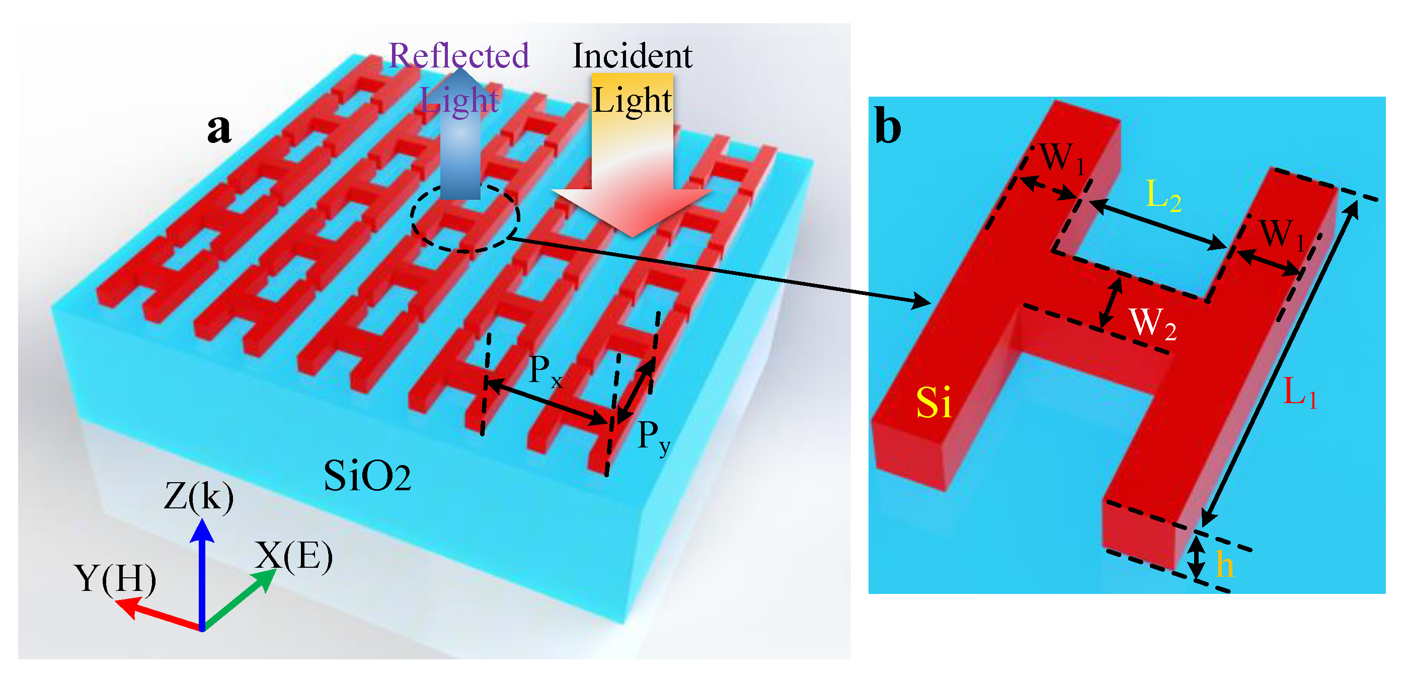
An all-dielectric color filter, based on a silicon nanoarray, is presented in this paper.
Figure 1 shows the device’s structure and details, consisting of an SiO
2 substrate and an array of a-Si nanostructure etched onto it. The collection consists of an H-type nanoresonator. The resonator is composed of two rectangular blocks: two parallel rectangular blocks with length
, width
, and height
, and one rectangular block with length and width, respectively. A rectangular block comprises two lines,
and
, which are perpendicular to the middle of two adjacent rectangular blocks (referred to as a vertical rectangular block in the text). We set the height of the array composed of H-type Si nanoresonators as
, the period in the
x-direction as
, the filling factor in the
x-direction as
, the period in the
y-direction as
, and the filling factor in the
y-direction as
. At the same time, we set the mesh accuracy of the “H” structure to 1 nm in
x,
y, and
z-direction.
Lumerical FDTD Solutions commercial software was used to analyze the optical properties of the nanoarray in this paper. The refractive index of material Si was obtained from Palik [
31], and the refractive index of SiO
2 substrate was 1.5. In the case of one H-type nanoresonator, the simulation area was defined by periodic boundary conditions along the
x and
y axes, the
z-axis by a perfect matching layer (PML), and the environmental medium was air (refractive index = 1). In this model, linearly polarized light sources are incident vertically along the z-axis from top to bottom (
K is the wave vector), and the electric field (
E) and magnetic field (
H), respectively, are arranged along the
x- and
y-axes.
To visualize the color change more intuitively, the reflectance spectrum data were converted into color coordinates through the color matching function that corresponds to the CIE1931 chromaticity diagram, where the coordinate points were calculated using the formula [
8], as follows:
The formula includes the simulated reflection spectrum (
), the relative spectral power distribution of the incident light (
), and the normalization factor (
).
are the standard tristimulus values, which are the color-matching functions.
are determined by the tristimulus values, converted from reflectance spectrum data. The wavelength ranges from 400 nm to 800 nm at 1 nm intervals. Using Formulas (2) and (3), the CIE1931 chromaticity diagram coordinates were obtained. In CIE1931, when the chromaticity coordinates
are in the horseshoe’s center, the corresponding fully unsaturated colors will be present, if the corresponding fully saturated colors are on edge. Using this feature, the saturation and change trend of colors can be seen intuitively.
3. Results and Discussion
Electric dipole (ED) and magnetic dipole (MD) resonances are generated when light is incident on the nanoresonator. For simple structures, such as nanospheres, previous analyses have shown that the relationship between the solid magnetic resonance in the visible range and the wavelength and system is defined by the association,
Where
,
, and
are the wavelength, refractive index, and the radius of the nanosphere, respectively [
26,
32]. According to the fundamental rule, one can achieve passive tunability by simply scaling the size of the sphere to perform a specific spectral response in the desired range [
33]. The H-type nanostructures described in this article are relatively complex. They cannot explain the relationship between the structure and the resonance wavelength as simply a nanosphere or provide a precise analytical solution. For this reason, we devised a set of parameters to analyze the optical characteristics of the H-type Si nanoarray, as follows:
,
,
,
,
. In the current study, we studied how each structural parameter affected the filter color, using the controlled variable method.
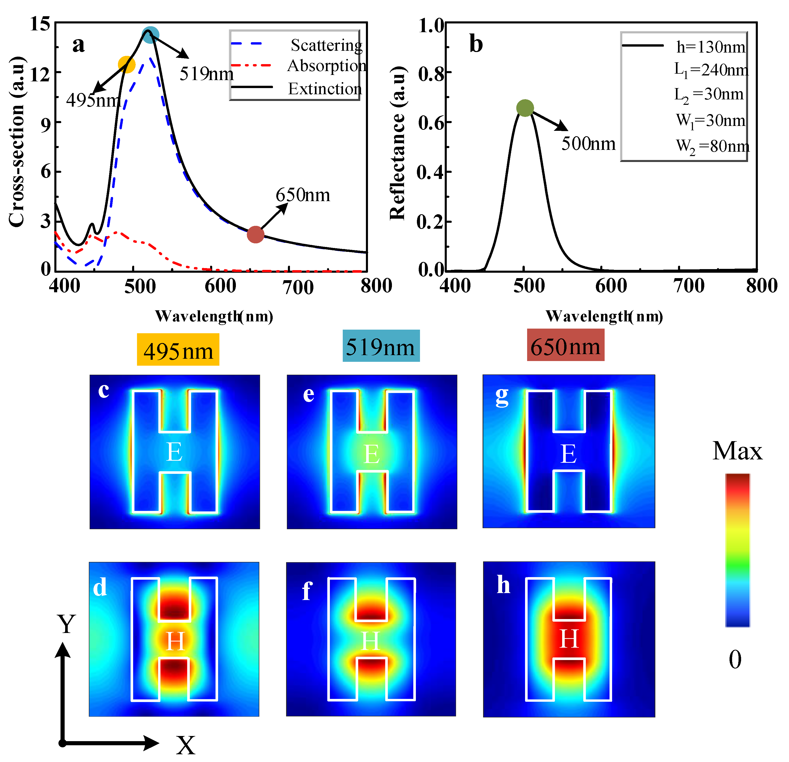
Figure 2b shows the reflection spectrum under the proposed parameters.
Figure 2a shows the proposed parameters’ extinction cross-section, absorption cross-section, and scattering cross-section. The extinction cross-section is the sum of the scattering cross-section and the absorption cross-section.
Figure 2a,b show that the spectrum’s reflection is mainly determined by scattering and that the electric field in the scattering spectrum at a wavelength of 495 nm (the position of the shoulder) is mainly distributed in the outer and inner side of the H-type long arm, and that the electric field in the scattering spectrum curve at a wavelength of 519 nm (the peak position) is mainly distributed in the inner side of the H-type long arm. The two different wavelengths of the different dipole resonance patterns work together to cause the high reflection peak at a wavelength of 500 nm in the reflection spectrum, in
Figure 2b.
Figure 2c–h shows the field distribution diagrams, resulting from the dipole resonance.
Figure 2c,d show the distribution of the electric field (
) and the magnetic field (
), at 495 nm. Generally, the electric field occurs on both sides of the H-type resonator in the x-direction and on the inner slits of two parallel rectangular blocks.
Figure 2g,h show electromagnetic field distributions with no resonance enhancement. In
Figure 2g, only the x-direction of the resonator exhibits electric field enhancement.
Figure 2h is in the vertical oblong block, and both sides of the y-direction show magnetic field enhancement. The analysis of the field distribution diagram in
Figure 2 shows that the resonance at 495 nm is MD resonance, and the resonance at 519 nm is ED resonance. MD resonance, ED resonance, and mutual coupling between the resonators are responsible for the resonance at 650 nm in the reflection spectrum. Therefore, if you want to change the resonance wavelength in the reflection spectrum, you must alter the structural parameters.
In addition, in
Figure 2a of the scattering spectrum, the MD resonance occurs at a wavelength of 495 nm, and the magnetic field is distributed on the inner side of the two long arms in the x-direction, as shown in
Figure 2c, indicating that the MD resonance occurs on the inner side of the two long arms. The ED resonance occurs at a wavelength of 519 nm, and the electric field is distributed on the upper and lower sides of the H-shaped crossbar, as shown in
Figure 2f, indicating that the ED resonance occurs on the upper and lower sides of the crossbar, and the ED and MD resonances will be coupled separately, resulting in a high reflection peak at a wavelength of 500 nm in the reflection spectrum.
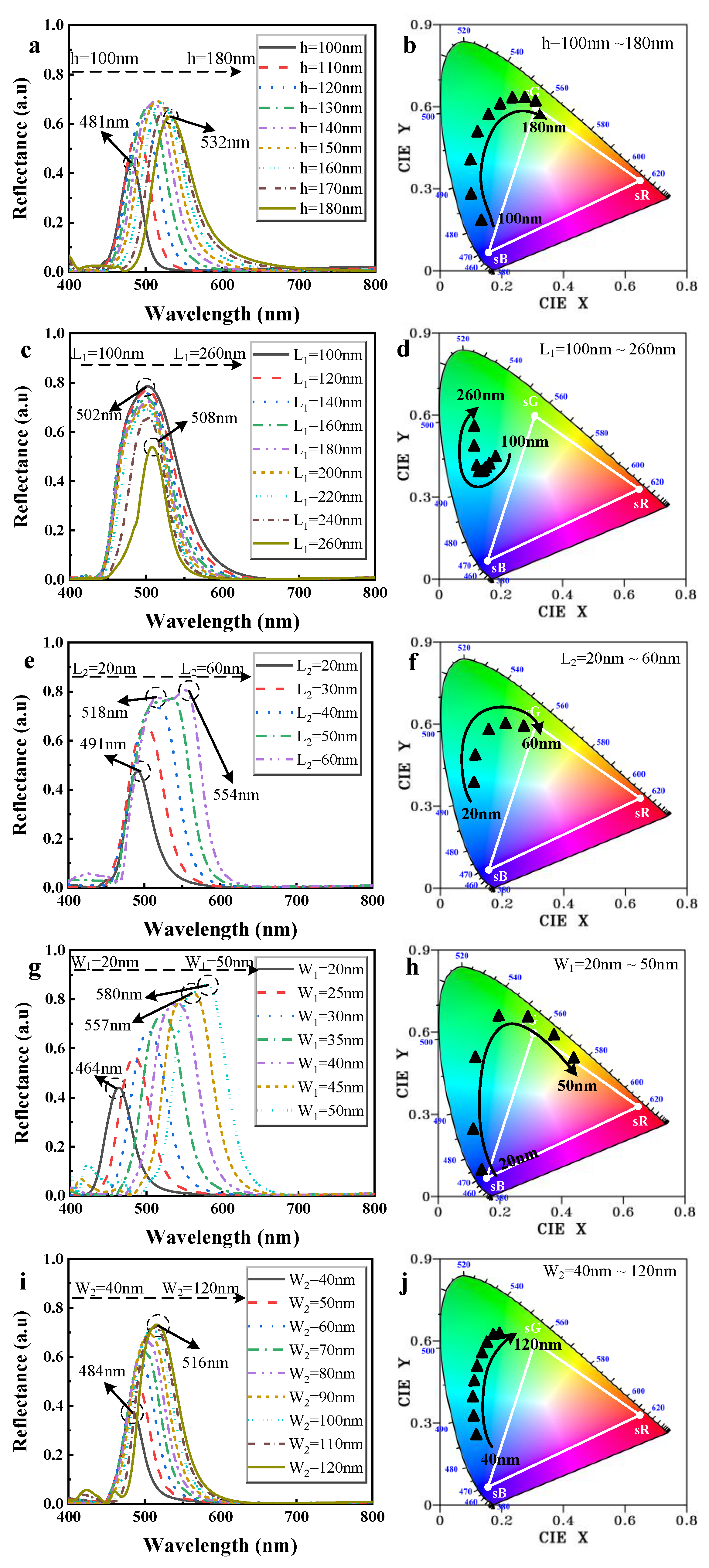
The controlled variable method was used to investigate the influence of each structural parameter on the resonance wavelength and filter color. In the first step, we analyzed the trends and the color change, based on the individual differences in parameter
. According to
Figure 3a, as
increases from 100 nm to 180 nm in 10 nm steps, the resonance peak is redshifted and increases gradually, and the full width at half maximum (FWHM) peak increases from 33 nm to 60.5 nm. Color brightness is affected by the resonance peak height. As the peak value rises, the color brightness increases. The position of the resonant peak determines the reflected color, and its FWHM determines the color saturation. The saturation of the color decreases as the FWHM increases.
Figure 3b is a CIE1931 chromaticity diagram, drawn after the reflectance spectrum in
Figure 3a was calculated using the color matching function. The coordinate points in
Figure 3b correspond to the reflection spectrum. Increasing the value of
gradually causes the color coordinates to move from the blue area to the green zone, indicating that the parameter effectively controls the filtered color. The generated color coordinate points are all outside the sRGB color gamut, confirming the high color saturation caused in the model.
Figure 3c shows the reflectance spectrum as 20 nm increments increase parameter
from 100 nm to 260 nm. By increasing
, the resonant peak in the reflection spectrum is redshifted from 502 nm to 508 nm, the height is gradually reduced, and the FWHM decreases from 85.5 nm to 39.5 nm.
Figure 3d shows that all of the coordinate points on the CIE1931 chromaticity diagram are outside the SRGB color gamut, indicating that the saturation is relatively high. However, as
increases, the color coordinate change range is minimal, demonstrating that
is not the main parameter affecting the reflected color. The reflectance spectrum is shown in
Figure 3e, when the size of
is changed.
Figure 3e shows that as
increases from 20 nm to 60 nm in 10 nm steps, the peak is redshifted, the peak increases, and the FWHM increases from 39.5 nm to 94 nm. Two resonance peaks appear at 518 nm and 554 nm when
. The reason is that when
is slight,
MD and
ED resonance occur at the same wavelength. The distance between the
ED resonance wavelength and the
MD resonance wavelength gradually increases as
increases, resulting in two peaks. The CIE1931 chromaticity diagram in
Figure 3f shows that all chromaticity coordinates are outside the SRGB color gamut. The color gradually changes from blue to green, with a wide color range. When
increases, the FWHM of the reflection peak also increases, resulting in a decrease in color saturation. Therefore,
is the most crucial color control parameter. In the H-type nanoresonator,
is the width of two parallel rectangular blocks.
Figure 3g shows the reflection spectrum produced by varying
. As
increases from 20 nm to 50 nm in 5 nm steps, the reflection spectrum’s peak is redshifted, the height gradually increases, and the FWHM also gradually increases from 41 nm to 75.5 nm. When
, there are two resonances at the 557 nm and 580 nm wavelengths. This is the exact reason for the two resonances when
. The parameter value is too large, so there is a significant difference between the
ED and
MD resonance wavelengths, which causes the resonance peak to split.
Figure 3h is the CIE1931 chromaticity diagram corresponding to
Figure 3g. The chromaticity coordinate point gradually moves from blue to orange with the increase in W1, and the color saturation gradually decreases with the rise in FWHM. The variation range of
in
Figure 3g is 20 nm~50 nm. Despite its small structural change, its range of color variations is quite extensive, so it can achieve all-light control even in visible light, showing that
has a remarkable ability to control reflected light.
Figure 3i shows the reflectance spectrum of parameter
increasing in 10 nm steps, from 40 nm to 120 nm. Increasing the value of
causes the resonant peak to be redshifted from 484 to 516 nm, and the height is markedly increased, while the FWHM increases from 33 to 57 nm. In
Figure 3j, the CIE chromaticity coordinate moves from blue to green as
increases, and the color change range is wide, showing that
can effectively control the reflected color.
As demonstrated in many articles, the nanospheres’ size can be scaled to obtain specific spectral responses within the required range [
29,
30]. In this study, we also mounted the proposed structure to observe its spectral response.
Table 1 shows the results of scaling the parameters, and
Figure 4a shows the simulated reflection spectrum of the parameters in
Table 1 and the corresponding CIE chromaticity diagram. The corresponding resonance peak band in
Table 1 gradually redshifts from 431 nm to 619 nm, and its peak value increases from
S(
1) to
S(
8).
Figure 4b shows an intuitive change in the CIE 1931 chromaticity coordinates. With the parameter increased, the color coordinates’ points span from blue to red, and they are all outside the sRGB color gamut. Therefore, it is possible to achieve high-saturation color filtering in the visible range by scaling the structure. Designed filters employ different heights for different colors, making it challenging to create a filter mosaic. In the proposed nanocross antenna, a wide range of colors is achieved with the same height, essential for high-density spectral filter mosaics [
15]. For this reason, when we simulated
Table 1, the height parameter
h was fixed at 141 nm, and the resulting reflection spectrum and CIE1931 chromaticity diagram are shown in
Figure 4c. As the parameter changes from
S(
1) to
S(
8), the peak is redshifted from 454 nm to 598 nm, and the height gradually increases until it reaches
S(
5), and then it decreases. The peak movement range of
Figure 4c is smaller than that of
Figure 4a, since the
h is fixed, while the peak change also differs from that of
Figure 4a.
Figure 4d shows the CIE chromaticity coordinate points that correspond to the reflection spectrum of
Figure 4c. The saturation levels are high and all the chromaticity coordinate points are outside of the sRGB color gamut. The color changes gradually from blue to red over a more extensive variation range, achieving complete light control in the visible light field and meeting the requirements of a high-density spectral filter.
Finally, the effect of the polarization angle of the incident light on the reflection spectrum and the filtered color was investigated, as shown in
Figure 5a,b. As the polarization angle of the incident light increases, the peak value of the reflection peak gradually decreases, and when the polarization angle is greater than 45°, a new main reflection peak at the new position wavelength of 582 nm and a new reflection secondary peak at the wavelength of 449 nm appear. With the increase in the polarization angle, the peak values of both the main and secondary reflection peaks increase. The CIE diagram shows that the color point is moving closer to the center of the CIE diagram, indicating that the color is becoming impure as the incident light polarization angle increases.
We then tried to change the angle of incidence in the y-direction on the reflection spectrum and the filtered color, by changing the angle of incidence from 0° to 60°. From the simulation of the reflection spectrum, we saw that as the angle of incidence increased from 0° to 60°, the resonance position remained unchanged, at 500 nm, and the resonance peak became two. From the CIE chromaticity diagram, we can see that as the angle of incidence in the y-direction increases from 0° to 60°, the filtered color changes from green to light blue, indicating that the structure has a good angle dependence.


