Article

Numerical and Experimental Study on Thermal Damage Induced by Medium—Infrared Laser

1
Joint Laboratory for Extreme Conditions Matter Properties, State Key Laboratory of Environmental-Friendly Energy Materials, Tianfu Institute of Research and Innovation, Southwest University of Science and Technology, Mianyang 621010, China
2
Research Centre of Laser Fusion, China Academy of Engineering Physics, Mianyang 621900, China
3
IFSA Collaborative Innovation Center, Shanghai Jiao Tong University, Shanghai 200240, China
4
Research Center for Photonic Technology, Fujian Provincial Key Laboratory for Advanced Micro−Nano Photonics Technology and Devices & Key Laboratory of Information Functional Material for Fujian Higher Education, Quanzhou Normal University, Quanzhou 362000, China
*
Authors to whom correspondence should be addressed.
Photonics 2022, 9(11), 838; https://doi.org/10.3390/photonics9110838
Submission received: 20 September 2022 / Revised: 21 October 2022 / Accepted: 1 November 2022 / Published: 8 November 2022

Abstract

:
We studied the laser-induced thermal damage on the surface of a single crystal silicon mirror illuminated by a mid-infrared intense laser. We used mid−infrared quasi-continuous wave lasers to irradiate the surface of the single−crystal silicon mirror. The power density of the irradiation process is 1 kW/cm2 to 17 kW/cm2, and the transient temperature field and thermal stress field under different laser fluxes were obtained. The simulation results show that we can calculate the thermal stress and temperature under laser irradiation. In addition, irradiance exceeding the corresponding breaking strength and melting point limit was obtained by the model. We can predict the irradiance that causes cracking and melting. There is little difference between experimental results and simulation results. On this basis, the thermal damage to the surface of the silicon wafer caused by continuous mid−infrared laser irradiation was studied.

1. Introduction

With the development of high−power laser technology, the damage of laser to optical surface has become increasingly serious. These problems have seriously restricted the development of high−power laser devices [1,2,3]. The power density or energy density will increase gradually when the high energy laser beam hits the surface of an optical component. When they increase to a certain extent, some nonlinear phenomena will occur on the optical surface, such as temperature rise, expansion, material sublimation and so on [4,5,6,7]. In addition, they may cause irreversible damage. Such phenomena are called laser induced optical surface or optical material damage [8,9]. Since the second year of the laser’s birth, researchers around the world have been studying the mechanism of laser and material damage [10,11,12]. In recent years, with the development of laser technology, high energy laser has been used in an increasingly wide range of applications in industries such as industry and military science, including laser ranging, laser guidance, laser blinding and laser weapons. Particularly, laser weapons have received a lot of attention and input in the field of high−energy lasers [13,14]. The common feature of these applications is that all optical components in the system must pass through a high-power density laser. In optical systems, the absorption coefficient of silicon at the wavelength of 1.2−7 μm and 25−300 μm is less than 10−7 cm−1. The absorbed laser energy is very small, and most of the laser energy is transmitted within these wavelength ranges [15]. In addition, monocrystalline silicon has the advantages of hard and brittle texture and small thermal deformation. It has been widely used in high power laser devices [16].
In high−power laser systems, the problem of damage to optical elements remains a key issue. The study of laser−induced damage behaviour of optical components has been a very active area in recent years, and due to the properties of silicon in optical systems, the damage mechanisms of laser−silicon interactions have been investigated. However, most of the research has focused on near−infrared wavelengths and pulsed lasers to investigate the thermal damage mechanism of silicon through simulations and experiments. In 2011, Wang et al. established a spatial axisymmetric finite element model for monocrystalline silicon irradiated by 1064 nm millisecond laser. The thermal stress damage induced by millisecond laser is studied by using this model. They obtained the transient temperature field and thermal stress field radiated by 2 ms laser when the laser flux was 254 J/cm2 [17]. In 2013, Wang et al. analyzed the thermal shock resistance of a solid subjected to sudden temperature changes in a hyperbolic, non−Fourier heat conduction framework [18]. In 2014, Choi et al. studied the calorific−value damage mechanism of silicon wafers under continuous near−infrared laser irradiation. The silicon wafer was irradiated by 1070 nm laser and the surface morphology of the sample was analyzed by optical microscope. In addition, the mechanism of thermal damage of silicon wafer is discussed through simulation based on heat conduction and thermoelastic model. In the same year, considering the transient free carrier density during irradiation, Rämer1 et al. theoretically studied the irradiation of 800 nm laser pulse on silicon using a dual temperature description. Bude et al. studied the damage precursors of silicon dioxide optical elements, and studied the damage mechanism involved and the process of reducing the damage precursors. Manyalibo et al. studied the use of infrared lasers in high−power laser systems for polishing, annealing, and micro−shaped fused silica surfaces [19,20,21,22]. In 2016, Victor reviewed and analyzed the photothermal conversion of single nanoparticle, its components and surrounding media in a wide pulse interval. Theoretical and experimental studies on heat exchange and heat conduction as well as heating process from femtosecond to continuous wave were carried out. In the same year, Doualle et al. carried out the thermodynamic numerical simulation of the physical process of CO2 laser irradiation on silicon based on the finite element method [23]. In 2017, Li et al. established the Si−CCD thermal stress coupling model under millisecond pulse laser radiation. They calculated the spatial and temporal distributions of temperature and stress fields on Si−CCD based on the four−dimensional heat conduction equations and thermoelastic equations [24]. In 2019, Zheng et al. used femtosecond pulsed lasers to irradiate silicon multilayered membranes and studied the ranges corresponding to various damage effects and threshold conditions. In addition, the physical mechanism of ultrafine laser on the membrane structure of typical imaging detectors was illustrated [25]. In 2022, kou et al. used the finite element method to develop a thermomechanical coupling model for laser irradiated CCDs, characterizing the damage threshold and damage characteristics of CCDs at the point damage, line damage, black and white split screen and complete damage stages. The results showed that the temperature rise effect of silicon substrate damage dominated in the transverse direction [26]. So far, there have been few researches on thermally induced damage caused of mid−infrared continuous lasers [27,28].
This paper studied the thermal damage mechanism of monocrystalline silicon by mid−infrared continuous laser irradiation. The output wavelength of the laser is 3.8 μm, the maximum laser power density is 17 kW/cm2, and the laser beam diameter is 1 mm. In addition, monocrystalline silicon by tincture was selected as the material in the experiment. We irradiated the sample continuously for 60 s with a continuous laser. The laser power density range is 1 kW/cm2 to 17 kW/cm2. In the calculation process, we first considered the plastic properties of silicon at high temperature. Secondly, the damage property of silicon was analyzed by temperature and thermal stress. In the experiment, we irradiated the monocrystalline silicon with a 3.8 μm high−frequency laser (wavelength 3.8 μm, pulse width 25–35 ns, spot size 0.3 mm), and found that the power density was 437,898 W/cm2, and the sample would be damaged. We analyzed the surface morphology of laser−irradiated silicon samples with EDS−SEM.

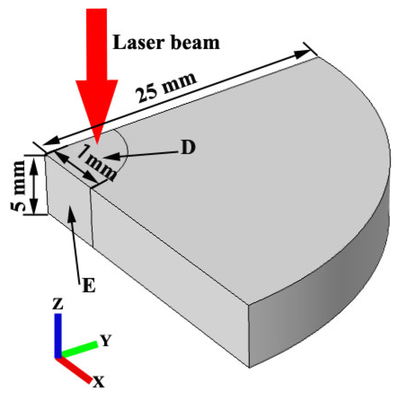
2. Geometric Model and Method

Figure 1 shows the geometric model of continuous laser irradiation of monocrystalline silicon. In this geometric model, we used a three−dimensional quarter−symmetric model to simulate the changes in the temperature field and thermal stress of the silicon wafer induced by continuous laser irradiation. The sample radius is r1 = 25 mm, and the thickness is D = 5 mm. In the simulation, the radius direction is set to the symmetric boundary condition. In this way, the model can be simulated according to the whole silicon chip during the calculation. In addition, in order to maintain the consistency between the constraints we applied and the experimental process, we set the sides of the silicon wafer as fixed constraints. The experimental parameters used in this model are shown in the following Table 1:
The change of thermal stress of laser irradiated samples is obtained by the solution of Duhamel−Neumann law. The law takes into account the effect of thermal expansion, as shown below [29,30,31]:
σ i j = C i j k l ε k l β i j ( T T 0 )
where σ is the stress, C is the elastic constant, ε is the strain, β is the thermal modulus, T is the temperature, and T0 is the initial temperature. In Formula (1), through the analysis of heat conduction theory, the transient temperature distribution T(x,y,z,t) can be obtained. The three−dimensional (3D−dimensional) differential equation of heat conduction is [32,33,34]:
ρ C p T t ( k T ) = Q
where ρ is the density, Cp is the heat capacity, k is the thermal conductivity, and Q is the heat source per unit volume. The intensity of the incident laser light can be expressed by a heat source Q per unit volume. In the process of simulation and experiment, the laser beam is Gaussian beam. Therefore, the intensity of incident laser light can be expressed as follows [35,36,37]:
Q = I 0 ( 1 R ) γ e x p ( γ z ) exp [ 2 ( x 2 + y 2 ) r 0 2 ]
where I0 is the intensity of the incident beam, R is the reflectivity, γ is the absorption coefficient, and r0 is the radius of the laser beam.
As shown in Figure 1, we used Comsol Multiphysics to simulate the laser−loaded photothermal multiphysics coupling model, where D is the heat source and E is the symmetric boundary condition. In addition, during the simulation, we used symmetric boundary conditions to simplify the model with a quarter symmetric model. Besides, we set the thickness of the optical element to 5 mm and the radius to 50 mm. The convection and radiation during simulation are as follows [38,39]:
n ( k T ) = h ( T a m b T ) + ε r a d σ S B ( T a m b 4 T 4 )
where n is the normal vector of the boundary, h is the convective heat transfer coefficient, T is the ambient temperature, ε is the emissivity, and σ is the Stefan−Boltzmann constant.

3. Analysis and Discussion

In this work, we first studied the temperature change of laser beam center at different laser power densities. Secondly, we considered the effects of practical applications of thermal convection and radiation. We chose to keep the laser on for 60 s until the stress and temperature reached saturation. In practice, however, shorter time exposures and higher laser irradiance may be of interest in military applications [40,41]. Even in this case, our computational simulation results were still available. When the irradiation lasted only a few milliseconds, the damage mechanism did not change.
Figure 2 shows the central temperature change curves of laser beam under 5000, 9000, 13,000 and 17,000 W/cm2 irradiation. At the beginning of laser irradiation, the temperature rises sharply due to convection and radiation. The highest temperature after 60 s is lower than the melting point of silicon wafer (1683.15 K). Therefore, no melting is expected under these conditions.
In this work, we simulated the distribution of stress in different directions and body stress under 17,000 W/cm2 laser power density irradiation. Figure 3a–d shows the typical stress of σxx, σyy, σzz and σv on Mises stresses on the surface of silicon samples, respectively. The value of the tensile stress shown is greater than zero and the compressive stress is less than zero. For the stresses σxx and σyy, the maximum compressive stress is located at the geometric center of the entire optical element which is the spot position [42]. Its value is 5.17 N/m2. On the other hand, the maximum stress of σzz is only 3 N/m2, which is relatively small. For the equivalent stress σv, the maximum tensile stress is located at the geometric center of the entire optical element. Its numerical is 3.66 N/m2.
In this study, we simulated silicon−based optical components with different radii and chose the energy radiated by laser beam to be 17,000 W/cm2. The laser beam is applied continuously for 60 s on a silicon wafer with a thickness of 5 mm. We simulated the temperature field of silicon wafers with different radii (10 mm, 15 mm, 20 mm, 25 mm). It can be observed the temperature change in the center of the wafer. Figure 4 shows the changes in the central temperature of silicon wafers with different radii after continuous 60 s laser irradiation. We can find that as the radius of the silicon chip increases, the temperature at the center of the silicon chip decreases. When the radius of the silicon wafer is small, the range of temperature variation is more significant. This is mainly due to the small radius of the silicon chip, which accumulates a lot of heat inside the silicon wafer. Silicon has very low thermal conductivity and little heat to the air [43,44,45]. As a result, the temperature at the center of the wafer varies significantly, while the temperature of the entire wafer can be higher. When the radius of the silicon wafer is larger, the temperature drop in the center of the silicon wafer is smaller. This is mainly due to the amount of heat absorbed inside the silicon wafer [46,47]. At this point, the total input energy is consistent with the radiation at a small radius, and the same heat is distributed over a larger area. The heat transferred to the air is still fixed. Therefore, the temperature in the center of the silicon chip will be relatively low, and the temperature distribution of the whole silicon chip will be relatively uniform.
In this work, we simulated silicon−based optical components with different thicknesses. In this study, the irradiation energy of laser beam is selected to be 17,000 W/cm2. The laser beam continuously acts on the silicon wafer with a radius of 25 mm for 60 s. The laser beam is also applied to silicon wafers of different thicknesses (2 mm, 3 mm, 4 mm, 5 mm). The chip has carried out the simulation of the temperature field to observe the temperature change in the center of the silicon chip [48]. Figure 5 shows the temperature change at the center of silicon wafers with different radii at the end of 60 s continuous irradiation of the laser beam. We can find that as the thickness of the silicon wafer gradually increases, the temperature at the center of the wafer will gradually decrease. When the thickness of the silicon wafer is small, the temperature variation range is more obvious. This is mainly due to the small thickness of the silicon wafer, which has low thermal conductivity and very limited heat transfer to the air [49,50,51]. A large amount of heat is accumulated in the center of the silicon wafer, so the difference in temperature at the center point of the silicon wafer is obvious. The entire silicon wafer can have a higher temperature. When the thickness of the silicon chip is large, the temperature at the center of the silicon chip decreases relatively small. This is mainly due to the amount of heat absorbed by the silicon wafer [52,53,54]. The total input energy is consistent with radiation with a smaller thickness. The same amount of heat will be distributed over a larger area [55]. Moreover, the transfer of heat to the air is still fixed. Therefore, the temperature in the center of the silicon wafer is relatively low, and the temperature distribution of the entire silicon wafer is relatively uniform.
In this work, we chose different beam radii to simulate the irradiation process of the same optical element. In this study, we chose a fixed sample size with a radius of 25 mm and a thickness of 5 mm. The total output energy of the laser is 17,000 W/cm2. We set different beam radii (0.5 mm, 1 mm, 2 mm, 4 mm laser beams) to achieve continuous action of the 60 s on the silicon wafer. By simulating the temperature field, the temperature variation of the silicon wafer center can be observed. Figure 6 shows the temperature change in the center of the silicon wafer when lasers with different beam radii are used for continuous irradiation for 60 s. We can find that when the spot radius is 0.1 mm, the temperature at the center of the silicon chip hardly rises. This is because although the input energy of the laser is high, the area of action is small [56]. This area of the laser beam is small, so the heat generated inside the silicon wafer is small. As a result, the temperature remains almost constant except in the center. When the laser beam radius increases to 0.5 mm, the heat flux generated inside the silicon wafer increases. The temperature in the center of the wafer is also higher, and the overall temperature of the wafer is going to go up a lot. As the spot radius increases to 1 mm and 4 mm, we find that the temperature difference at the center of the silicon wafer is very small, only a few tens of kelvin. This is due to the small difference in heat flux generated inside the silicon wafer at this time.
For the laser power densities of 1000, 5000, 9000, 13,000 and 17,000 W/cm2, the change of the von mises stress (σv) at the center of the laser beam is shown in Figure 7. In order to predict the occurrence of cracks, stress changes are compared with fracture strength. The fracture strength of silicon generally depends on the size and thickness of the sample. In addition, due to brittle fracture behavior, the fracture strength has a large deviation [57]. Paul et al. investigated the fracture strength of silicon of different thickness using Weibull and the normal model. The breaking strength of silicon with a thickness of 525 μm ranges from 96 to 386 MPa. It has a nearly normal distribution (average fracture strength of 222 MPa, standard deviation of 70 MPa). As a result, a breaking strength range of 222 ± 20 MPa is adopted, which has a high probability density [58,59].
In this study, we tested the damage of a monocrystalline silicon mirror with a radius of 25 mm, a thickness of 5 mm. During the experiment, we selected a mid−infrared Quasi−Continuous Wave(QCW) laser for testing. The laser works in TEM00 mode and laser pulses. The width τ = 25−30 ns, the repetition frequency is 17 kHz, and the average power density is 437,898 kW/cm2. We used EDS−SEM to observe the typical damage morphology on the surface of single crystal silicon, as shown in Figure 8a. We can find traces of ablation and melting in the center of the spot. At the edge of the ablative area, there are cracks generated during cooling and solidification. In addition, we can find that there are a lot of small particles around the ablation area, which is mainly caused by the huge temperature gradient along the radial direction [60,61]. In Figure 8b, we simulated the experiment process with the same power density. We can find that the temperature at the center of the silicon mirror can reach 1849.07 K, which is much higher than the melting point 1683.15 K of silicon. The simulation results are consistent with our experimental results. In addition, after the laser loading process, the temperature of the silicon mirror edge is only about 600 K, and the lowest temperature is 551.872 K. The difference with the central temperature is about 1300 K, which is consistent with our experimental situation.
In addition, we also selected a mid−infrared Continuous Wave(CW) laser to test the damage of a monocrystalline silicon mirror with a radius of 25 mm, a thickness of 5 mm during the experiment. The laser power is 1500 W and the laser focused spot size is approximately 3 mm. We also used EDS−SEM to observe the typical damage morphology on the surface of the monocrystalline silicon, as shown in Figure 9a. We can also observe traces of ablation and melting at the spot. Numerous ablation holes are generated throughout the ablation area during cooling and solidification. In addition, the largest ablation holes are generated in the centre of the ablation area, mainly because of the temperature gradient in the radial direction [61]. In Figure 9b, we simulated the experiment process with the same power density. In the simulation, we replaced the heat source with a surface heat source. We can find that the temperature at the center of the silicon mirror can reach 1831.62 K, which is much higher than the melting point 1683.15 K of silicon. The simulation results are consistent with our experimental results as shown in Figure 9a. In addition, after the laser loading process, the temperature of the silicon mirror edge is only about 800 K, and the lowest temperature is 763.048 K. The difference with the central temperature is about 1068 K. When QCW and CW lasers irradiate the surface of optical components, the physical mechanism is approximately the same, and both are thermally induced damage. The specific mechanism is as follows: when QCW and CW lasers irradiate the surface of the optical element, the optical element absorbs the energy of the laser and the energy is converted from light energy to heat energy. When a defect exists in an optical element, it creates a temperature gradient difference within it. When the energy absorbed by the element reaches the material’s own limit, it causes damage to the element, which leads to thermally induced damage [62,63,64]. Hence, the effect of selecting QCW and CW lasers is the same in terms of average power during simulation and experiment. Therefore, our simulation results can provide a theoretical basis for thermal stress damage in silicon and predict the results of laser damage threshold testing.

4. Conclusions

The laser−induced thermal damage on the surface of the silicon wafer exposed to the mid−infrared wavelength quasi−connected laser is studied through simulation and experiment. The planar sample of monocrystalline silicon is irradiated by a quasi−continuous laser for 60 s under different irradiation conditions. The surface morphology of the laser—irradiated samples is analyzed by SEM. In addition, these values are compared with numerical predictions to verify that the observed damage (e.g., cracks and melting) is caused by thermal stress and high temperature. This numerical calculation model is based on heat transfer and thermoelasticity. The irradiance of crack is predicted by determining the irradiance of von Mises stress in the range of fracture strength. The calculated temperature exceeds the melting point of 1683.15 K. The predicted results are consistent with the experimental results. Based on these studies, the laser-induced thermal damage on the surface of the silicon wafer exposed to the quasi-continuous laser is determined.

Author Contributions

Z.L., Q.L., Z.Y. and P.W.: Conceptualization, Formal analysis, Investigation, Data curation, Writing—original draft, Writing—review & editing. Y.Z.: Conceptualization, Formal analysis, Investigation, Data curation, Funding acquisition. T.S. and X.Y.: Conceptualization, Formal analysis, Investigation, Data curation; L.S., and K.W.: Conceptualization, Formal analysis, Investigation. W.Z.: Conceptualization, Formal analysis. All authors have read and agreed to the published version of the manuscript.

Funding

The work is supported by the National Natural Science Foundation of China (NSFC) (61705204, 61705206, 62005258, and 61805221). Laser Fusion Research Center Funds for Young Talents (RCFPD3−2019−2) and Foundation of Science and Technology on Plasma Physics Laboratory of China Academy of Engineering Physics (2018).

Institutional Review Board Statement

Not applicable.

Informed Consent Statement

Not applicable.

Data Availability Statement

Publicly available datasets were analyzed in this study. This data can be found here: [https://www.lumerical.com/] (accessed on 1 January 2020).

Conflicts of Interest

The authors declare that they have no known competing financial interest or personal relationships that could have appeared to influence the work reported in this paper.

References

  1. Jauregui, C.; Limpert, J.; Tünnermann, A. High-power fibre lasers. Nat. Photonics 2013, 11, 861–867. [Google Scholar] [CrossRef]
  2. Wang, D.Y.; Yi, Z.; Ma, G.L.; Dai, B.; Yang, J.B.; Zhang, J.F.; Yu, Y.; Liu, C.; Wu, X.W.; Bian, Q. Two channels photonic crystal fiber based on surface plasmon resonance for magnetic field and temperature dual-parameter sensing. Phys. Chem. Chem. Phys. 2022, 24, 21233. [Google Scholar] [CrossRef] [PubMed]
  3. Li, L.; Gao, H.; Liu, G.; Wang, S.; Yi, Z.; Wu, X.; Yang, H. Synthesis of carnation flower-like Bi2O2CO3 photocatalyst and its promising application for photoreduction of Cr(VI). Adv. Powder Technol. 2022, 33, 103481. [Google Scholar] [CrossRef]
  4. De Araújo, C.B.; Gomes, A.S.L.; Boudebs, G. Techniques for nonlinear optical characterization of materials: A review. Rep. Prog. Phys. 2016, 79, 036401. [Google Scholar] [CrossRef] [PubMed] [Green Version]
  5. Chen, H.; Chen, Z.; Yang, H.; Wen, L.; Yi, Z.; Zhou, Z.; Dai, B.; Zhang, J.; Wu, X.; Wu, P. Multi-mode surface plasmon resonance absorber based on dart-type single-layer graphene. RSC Adv. 2022, 12, 7821–7829. [Google Scholar] [CrossRef]
  6. Lin, X.; Li, M.; Li, Y.J.; Chen, W. Enhancement of the catalytic activity of ordered mesoporous TiO2 by using carbon fiber support and appropriate evaluation of synergy between surface adsorption and photocatalysis by Langmuir-Hinshelwood (L-H) integration equation. RSC Adv. 2015, 5, 105227–105238. [Google Scholar] [CrossRef]
  7. Cao, W.X.; Lin, L.; Qi, H.F.; He, Q.; Wu, Z.J.; Wang, A.Q.; Luo, W.H.; Zhang, T. In-situ synthesis of single-atom Ir by utilizing metal-organic frameworks: An acid-resistant catalyst for hydrogenation of levulinic acid to gamma-valerolactone. J. Catal. 2019, 373, 161–172. [Google Scholar] [CrossRef] [Green Version]
  8. Li, H.; Li, G.; Wu, K.; Zhang, B.; Yang, Z.; Pan, S. BaB2S4: An Efficient and Air-stable Thioborate as Infrared Nonlinear Optical Material with High Laser Damage Threshold. Chem. Mater. 2018, 30, 7428–7432. [Google Scholar] [CrossRef]
  9. Shangguan, Q.Y.; Chen, Z.H.; Yang, H.; Cheng, S.B.; Yang, W.X.; Yi, Z.; Wu, X.W.; Wang, S.F.; Yi, Y.G.; Wu, P.H. Design of Ultra-Narrow Band Graphene Refractive Index Sensor. Sensors 2022, 22, 6483. [Google Scholar] [CrossRef]
  10. Emmony, D. Laser mirror damage in germanium at 10.6 μm. Appl. Phys. Lett. 1973, 23, 598. [Google Scholar] [CrossRef]
  11. Laurence, T.; Bude, J.; Ly, S.; Shen, N.; Feit, M. Extracting the distribution of laser damage precursors on fused silica surfaces for 351 nm, 3 ns laser pulses at high fluences (20–150 J/cm2). Opt. Express 2012, 20, 11561. [Google Scholar] [CrossRef]
  12. Luo, W.H.; Cao, W.X.; Bruijnincx, P.C.A.; Lin, L.; Wang, A.Q.; Zhang, T. Zeolite-supported metal catalysts for selective hydrodeoxygenation of biomass-derived platform molecules. Green Chem. 2019, 21, 3744–3768. [Google Scholar] [CrossRef]
  13. Couairon, A.; Sudrie, L.; Franco, M.; Prade, B.; Mysyrowicz, A. Filamentation and damage in fused silica induced by tightly focused femtosecond laser pulses. Phys. Rev. B 2005, 71, 125435. [Google Scholar] [CrossRef]
  14. Michael, A.S.; Kirchner, G.; Koidl, F.; Wang, P.; Jilete, B.; Flohrer, T. Daylight space debris laser ranging. Nat. Commun. 2020, 11, 3735. [Google Scholar] [CrossRef]
  15. Chandler-Horowitz, D.; Amirtharaj, P.M. High-accuracy, midinfrared (450 cm−1 ≤ ω ≤ 4000 cm-1) refractive index values of silicon. J. Appl. Phys. 2005, 97, 123526. [Google Scholar] [CrossRef]
  16. Fu, C.; Zhang, Z. Nanoscaleradiation heat transferfor silicon at different doping levels. Int. J. Heat Mass Transf. 2006, 49, 1703–1718. [Google Scholar] [CrossRef]
  17. Wang, X.; Qin, Y.; Wang, B.; Zhang, L.; Shen, Z.H.; Lu, J.; Ni, X.W. Numerical and experimental study of the thermal stress of silicon induced by a millisecond laser. Appl. Opt. 2011, 50, 3725–3732. [Google Scholar] [CrossRef] [PubMed]
  18. Wang, B.L.; Li, J.E. Thermal shock resistance of solids associated with hyperbolic heat conduction theory. Proc. R. Soc. A Math. Phys. Eng. Sci. 2013, 469, 20120754. [Google Scholar] [CrossRef]
  19. Choi, S.; Jhang, K. Thermal damages on the surface of a silicon wafer induced by a near-infrared laser. Opt. Eng. 2014, 53, 017103. [Google Scholar] [CrossRef] [Green Version]
  20. Rämer, A.; Osmani, O.; Rethfeld, B. Laser damage in silicon: Energy absorption, relaxation, and transport. J. Appl. Phys. 2014, 116, 053508. [Google Scholar] [CrossRef]
  21. Exarhos, G.; Gruzdev, V.; Menapace, J.; Ristau, D.; Soileau, M.; Bude, J.; Miller, P.; Shen, N.; Suratwala, T.; Laurence, T.; et al. Silica laser damage mechanisms, precursors and their mitigation. In Laser-Induced Damage in Optical Materials: 2014; SPIE: Boulder, CO, USA, 2014; Volume 9237, p. 92370S. [Google Scholar] [CrossRef]
  22. Matthews, M.; Yang, S.; Shen, N.; Elhadj, S.; Raman, R.; Guss, G.; Bass, I.; Nostrand, M.; Wegner, P. Micro-Shaping, Polishing, and Damage Repair of Fused Silica Surfaces Using Focused Infrared Laser Beams. Adv. Eng. Mater. 2015, 17, 247–252. [Google Scholar] [CrossRef]
  23. Doualle, T.; Gallais, L.; Cormont, P.; Hébert, D.; Combis, P.; Rullier, J. Thermo-mechanical simulations of CO2 laser–fused silica interactions. J. Appl. Phys. 2016, 119, 113106. [Google Scholar] [CrossRef]
  24. Li, M.; Jin, G.; Tan, Y. Simulation of the Si-CCD irradiated by millisecond pulse laser. Optik Int. J. Light Electron. Opt. 2017, 131, 67–71. [Google Scholar] [CrossRef]
  25. Zheng, C.; Shao, J.; Li, X.; Wang, H.; Wang, C.; Chen, F.; Wang, T.; Guo, J. Femtosecond pulsed laser induced damage characteristics on Si-based multi-layer film. Chin. Opt. Lett. 2019, 12, 371–381. [Google Scholar] [CrossRef]
  26. Kou, Z.; Li, Y.; Wang, G.; Li, K.; Hou, Y.; Xie, X.; Yu, Y.; Wang, Y.; Lu, Z. Temporal evolution characteristics and mechanism analysis of CCD breakdown induced by nanosecond and picosecond pulse lasers. Optik 2022, 162, 169313. [Google Scholar] [CrossRef]
  27. Sun, L.; Huang, J.; Liu, H.; Ye, X.; Wu, J.; Jiang, X.; Yang, L.; Zheng, W.; Wu, W. Combination of reaction ion etching and dynamic chemical etching for improving laser damage resistance of fused silica optical surfaces. Opt. Lett. 2016, 41, 4464–4467. [Google Scholar] [CrossRef]
  28. Liu, X.; Lu, X.; Wen, P.; Shu, X.; Chi, F. Synthesis of ultrasmall silica nanoparticles for application as deep-ultraviolet antireflection coatings. Appl. Surf. Sci. 2017, 420, 180–185. [Google Scholar] [CrossRef]
  29. Cheng, Z.; Liao, J.; He, B.; Zhang, F.; Zhang, F.; Huang, X.; Zhou, L. One-Step Fabrication of Graphene Oxide Enhanced Magnetic Composite Gel for Highly Efficient Dye Adsorption and Catalysis. ACS Sustain. Chem. Eng. 2015, 3, 1677–1685. [Google Scholar] [CrossRef]
  30. Li, Y.; Li, M.; Xu, P.; Tang, S.; Liu, C. Efficient photocatalytic degradation of acid orange 7 over N-doped ordered mesoporous titania on carbon fibers under visible-light irradiation based on three synergistic effects. Appl. Catal. A Gen. 2016, 524, 163–172. [Google Scholar] [CrossRef]
  31. Cai, L.; Zhang, Z.; Xiao, H.; Chen, S.; Fu, J. An eco-friendly imprinted polymer based on graphene quantum dots for fluorescent detection of p-nitroaniline. RSC Adv. 2019, 9, 41383–41391. [Google Scholar] [CrossRef] [Green Version]
  32. Lv, P.; Xie, D.; Zhang, Z. Magnetic carbon dots based molecularly imprinted polymers for fluorescent detection of bovine hemoglobin. Talanta 2018, 188, 145–151. [Google Scholar] [CrossRef] [PubMed]
  33. Liu, Y.; Bo, M.; Yang, X.; Zhang, P.; Sun, C.Q.; Huang, Y. Size modulation electronic and optical properties of phosphorene nanoribbons: DFT–BOLS approximation. Phys. Chem. Chem. Phys. 2017, 19, 5304–5309. [Google Scholar] [CrossRef] [PubMed]
  34. Long, F.; Zhang, Z.; Wang, J.; Yan, L.; Zhou, B. Cobalt-nickel bimetallic nanoparticles decorated graphene sensitized imprinted electrochemical sensor for determination of octylphenol. Electrochim. Acta 2015, 168, 337–345. [Google Scholar] [CrossRef]
  35. Zheng, Z.; Luo, Y.; Yang, H.; Yi, Z.; Zhang, J.; Song, Q.; Yang, W.; Liu, C.; Wu, X.; Wu, P. Thermal tuning of terahertz metamaterial properties based on phase change material vanadium dioxide. Phys. Chem. Chem. Phys. 2022, 24, 8846–8853. [Google Scholar] [CrossRef] [PubMed]
  36. Zhou, F.; Qin, F.; Yi, Z.; Yao, W.-T.; Liu, Z.; Wu, X.; Wu, P. Ultra-wideband and wide-angle perfect solar energy absorber based on Ti nanorings surface plasmon resonance. Phys. Chem. Chem. Phys. 2021, 23, 17041–17048. [Google Scholar] [CrossRef] [PubMed]
  37. Deng, Y.; Cao, G.; Wu, Y.; Zhou, X.; Liao, W. Theoretical Description of Dynamic Transmission Characteristics in MDM Waveguide Aperture-Side-Coupled with Ring Cavity. Plasmonics 2015, 10, 1537–1543. [Google Scholar] [CrossRef]
  38. Zhang, Z.; Cai, R.; Long, F.; Wang, J. Development and application of tetrabromobisphenol A imprinted electrochemical sensor based on graphene/carbon nanotubes three-dimensional nanocomposites modified carbon electrode. Talanta 2015, 134, 435–442. [Google Scholar] [CrossRef]
  39. Lin, X.; Li, Y.J.; Chen, F.T.; Xu, P.; Li, M. Facile synthesis of mesoporous titanium dioxide doped by Ag-coated graphene with enhanced visible-light photocatalytic performance for methylene blue degradation. RSC Adv. 2017, 7, 25314–25324. [Google Scholar] [CrossRef] [Green Version]
  40. Li, J.; Jiang, J.; Xu, Z.; Liu, M.; Tang, S.; Yang, C.; Qian, D. Facile synthesis of Ag@Cu2O heterogeneous nanocrystals decorated N-doped reduced graphene oxide with enhanced electrocatalytic activity for ultrasensitive detection of H2O2. Sens. Actuators B Chem. 2018, 260, 529–540. [Google Scholar] [CrossRef]
  41. Zhao, F.; Lin, J.; Lei, Z.; Yi, Z.; Qin, F.; Zhang, J.; Liu, L.; Wu, X.; Yang, W.; Wu, P. Realization of 18.97% theoretical efficiency of 0.9 μm thick c-Si/ZnO heterojunction ultrathin-film solar cells via surface plasmon resonance enhancement. Phys. Chem. Chem. Phys. 2022, 24, 4871–4880. [Google Scholar] [CrossRef]
  42. Deng, Y.; Cao, G.; Yang, H.; Zhou, X.; Wu, Y. Dynamic Control of Double Plasmon-Induced Transparencies in Aperture-Coupled Waveguide-Cavity System. Plasmonics 2018, 13, 345–352. [Google Scholar] [CrossRef]
  43. Tang, N.; Li, Y.; Chen, F.; Han, Z. In situ fabrication of a direct Z-scheme photocatalyst by immobilizing CdS quantum dots in the channels of graphene-hybridized and supported mesoporous titanium nanocrystals for high photocatalytic performance under visible light. RSC Adv. 2018, 8, 42233–42245. [Google Scholar] [CrossRef] [PubMed] [Green Version]
  44. Li, J.; Jiang, J.; Zhao, D.; Xu, Z.; Liu, M.; Liu, X.; Tong, H.; Qian, D. Novel hierarchical sea urchin-like Prussian blue@palladium core–shell heterostructures supported on nitrogen-doped reduced graphene oxide: Facile synthesis and excellent guanine sensing performance. Electrochim. Acta 2020, 330, 135196. [Google Scholar] [CrossRef]
  45. He, J.; Qian, T.; Cai, C.; Xiang, X.; Li, S.; Zu, X. Nickel-Based Selenides with a Fractal Structure as an Excellent Bifunctional Electrocatalyst for Water Splitting. Nanomaterials 2022, 12, 281. [Google Scholar] [CrossRef] [PubMed]
  46. Xiao, L.; Zhang, Q.I.; Chen, P.; Chen, L.; Ding, F.; Tang, J.; Li, Y.J.; Au, C.T.; Yin, S.F. Copper-mediated metal-organic framework as efficient photocatalyst for the partial oxidation of aromatic alcohols under visible-light irradiation: Synergism of plasmonic effect and schottky junction. Appl. Catal. B Environ. 2019, 248, 380–387. [Google Scholar] [CrossRef]
  47. Zheng, Z.; Zheng, Y.; Luo, Y.; Yi, Z.; Zhang, J.; Liu, Z.; Yang, W.; Yu, Y.; Wu, X.; Wu, P. A switchable terahertz device combining ultra-wideband absorption and ultra-wideband complete reflection. Phys. Chem. Chem. Phys. 2022, 24, 2527–2533. [Google Scholar] [CrossRef]
  48. Lin, X.; Du, S.W.; Li, C.H.; Li, G.J.; Li, Y.J.; Chen, F.T.; Fang, P.F. Consciously constructing the robust NiS/g-C3N4 hybrids for enhanced photocatalytic hydrogen evolution. Catal. Lett. 2020, 150, 1898–1908. [Google Scholar] [CrossRef]
  49. Chen, P.; Liu, F.; Ding, H.; Chen, S.; Chen, L.; Li, Y.-J.; Au, C.-T.; Yin, S.-F. Porous double-shell CdS@C3N4 octahedron derived by in situ supramolecular self-assembly for enhanced photocatalytic activity. Appl. Catal. B Environ. 2019, 252, 33–40. [Google Scholar] [CrossRef]
  50. Wu, X.; Zheng, Y.; Luo, Y.; Zhang, J.; Yi, Z.; Wu, X.; Cheng, S.; Yang, W.; Yu, Y.; Wu, P. A four-band and polarization-independent BDS-based tunable absorber with high refractive index sensitivity. Phys. Chem. Chem. Phys. 2021, 23, 26864–26873. [Google Scholar] [CrossRef]
  51. Liu, H.; Wang, Q.; Zhang, F. Preparation of Fe3O4@SiO2@ P(AANa-co-AM) Composites and Their Adsorption for Pb(II). ACS Omega 2020, 5, 8816–8824. [Google Scholar] [CrossRef] [Green Version]
  52. Cao, G.; Li, H.; Deng, Y.; Zhan, S.; He, Z.; Li, B. Systematic Theoretical Analysis of Selective-Mode Plasmonic Filter Based on Aperture-Side-Coupled Slot Cavity. Plasmonics 2014, 9, 1163–1169. [Google Scholar] [CrossRef]
  53. Cheng, T.; Gao, H.; Liu, G.; Pu, Z.; Wang, S.; Yi, Z.; Wu, X.; Yang, H. Preparation of core-shell heterojunction photocatalysts by coating CdS nanoparticles onto Bi4Ti3O12 hierarchical microspheres and their photocatalytic removal of organic pollutants and Cr(VI) ions. Colloids Surf. A Physicochem. Eng. Asp. 2021, 633, 127918. [Google Scholar] [CrossRef]
  54. Cai, C.; Han, S.B.; Zhang, X.T.; Yu, J.X.; Xiang, X.; Yang, J.; Qiao, L.; Zu, X.T.; Chen, Y.Z.; Li, S.A. Ultrahigh oxygen evolution reaction activity in Au doped co-based nanosheets. RSC Adv. 2022, 12, 6205–6213. [Google Scholar] [CrossRef] [PubMed]
  55. Long, F.; Wang, J.; Zhang, Z.; Yan, L. Magnetic imprinted electrochemical sensor combined with magnetic imprinted solid-phase extraction for rapid and sensitive detection of tetrabromobisphenol S. J. Electroanal. Chem. 2016, 777, 58–66. [Google Scholar] [CrossRef]
  56. Gu, Y.F.; Guo, B.B.; Yi, Z.; Wu, X.W.; Zhang, J.; Yang, H. Synthesis of a Self-assembled Dual Morphologies Ag-NPs/SrMoO4 Photocatalyst with LSPR Effect for the Degradation of Methylene Blue Dye. ChemistrySelect 2022, 7, e202201274. [Google Scholar] [CrossRef]
  57. Li, L.; Sun, X.; Xian, T.; Gao, H.; Wang, S.; Yi, Z.; Wu, X.; Yang, H. Template-free synthesis of Bi2O2CO3 hierarchical nanotubes self-assembled from ordered nanoplates for promising photocatalytic applications. Phys. Chem. Chem. Phys. 2022, 24, 8279–8295. [Google Scholar] [CrossRef]
  58. Bacar, Z. Modeling of CW laser diode irradiation of amorphous silicon films. Appl. Surf. Sci. 2011, 257, 5127–5131. [Google Scholar] [CrossRef]
  59. Paul, I. Statistical fracture modelling of silicon with varying thickness. Acta Mater. 2006, 54, 3991–4000. [Google Scholar] [CrossRef]
  60. Li, L.; Gao, H.; Yi, Z.; Wang, S.; Wu, X.; Li, R.; Yang, H. Comparative investigation on synthesis, morphological tailoring and photocatalytic activities of Bi2O2CO3 nanostructures. Colloids Surf. A Physicochem. Eng. Asp. 2022, 644, 128758. [Google Scholar] [CrossRef]
  61. Gu, Y.F.; Guo, B.B.; Yi, Z.; Wu, X.W.; Zhang, J.; Yang, H. Morphology modulation of hollow-shell ZnSn(OH)6 for enhanced photodegradation of methylene blue. Colloids Surf. A Physicochem. Eng. Asp. 2022, 653, 129908. [Google Scholar] [CrossRef]
  62. Tang, B.; Ren, Y. Tunable and switchable multi-functional terahertz metamaterials based on a hybrid vanadium dioxide–graphene integrated configuration. Phys. Chem. Chem. Phys. 2022, 24, 8408–8414. [Google Scholar] [CrossRef] [PubMed]
  63. Drake, R.A.; Kyle, R.P.K.; Lai, Y.; Wang, Z.; Cosmin, I.B.; Enam, A.C. Femtosecond laser damage of germanium from near- to mid-infrared wavelengths. Opt. Lett. 2018, 43, 3702. [Google Scholar] [CrossRef]
  64. Veres, I.; Berer, T.; Burgholzer, P. Numerical modeling of thermoelastic generation of ultrasound by laser irradiation in the coupled thermoelasticity. Ultrasonics 2013, 53, 141–149. [Google Scholar] [CrossRef] [PubMed]
Figure 1. Schematic diagram of simulation model. The symbol “D” denotes the heat source volume, and the symbol “E” indicates the symmetric boundary.
Photonics 09 00838 g001
Figure 2. Simulation results of wafer center temperature under power density of 5000, 9000, 13,000 and 17,000 W/cm2.
Photonics 09 00838 g002
Figure 3. (ad) are the simulation results of the typical stress σxx, σyy, σzz and σv (von mises stress) curves of the silicon wafer surface under 17,000 W/cm2 laser irradiation for 60 s, respectively.
Photonics 09 00838 g003
Figure 4. (ad) are the temperature change in the center of silicon wafers with different radii (10 mm, 15 mm, 20 mm, 25 mm) at the end of 60 s continuous laser beam irradiation, respectively.
Photonics 09 00838 g004
Figure 5. (ad) are the temperature changes in the center of silicon wafers with different thicknesses (2 mm, 3 mm, 4 mm, 5 mm) at the end of continuous laser beam irradiation for 60 s, respectively.
Photonics 09 00838 g005
Figure 6. (ad) are the schematic diagram of the temperature change in the center of the silicon wafer when lasers with different beam radii (0.5 mm, 1 mm, 2 mm, 4 mm) are continuously irradiated for 60 s, respectively.
Photonics 09 00838 g006
Figure 7. Schematic diagram of the variation of the Von Mis stress (σv) at the center of the laser beam at the laser power densities of 1000, 5000, 9000, 13,000 and 17,000 W/cm2.
Photonics 09 00838 g007
Figure 8. (a) is our use of EDS-SEM to observe the typical damage morphology of the single crystal silicon surface irradiated by quasi−continuous wave laser, and (b) is the simulation of the experimental process.
Photonics 09 00838 g008
Figure 9. (a) is our use of EDS−SEM to observe the typical damage morphology of the single crystal silicon surface irradiated by continuous wave laser, and (b) is the simulation of the experimental process.
Photonics 09 00838 g009
Table 1. Thermodynamic parameters of silicon at the wavelength of 3.8 μm.
Thermodynamic Parameters of Silicon Materials
SiSolidLiquid
Density (kg/cm3)2330 − 2.19 × 10⁻² × T2330 − 2.19 × 10⁻² × T − 1.21 × 10⁻⁵ × T2
Thermal conductivity (W/(m*K))22.23 + 422.52 × exp(−T/255.45)62
Heat capacity (J/kg*K)352.43 + 1.78 × T − 2.21 × 10⁻³ × T2 + 1.3 × 10⁻⁶ × T3 − 2.83 × 10⁻¹⁰ × T41021.84
Absorption coefficient (1/m)1023 × (T/273)48.6 × 107
Reflectivity0.080.72
Young’s modulus (Gpa)107
Thermal expansion coefficient (1/K)2 × 10−5
Poisson’s ratio0.28
Publisher’s Note: MDPI stays neutral with regard to jurisdictional claims in published maps and institutional affiliations.

