Review

Silicon-Based Graphene Electro-Optical Modulators

1
State Key Laboratory of Advanced Optical Communications System and Networks, School of Electronics, Peking University, Beijing 100871, China
2
Frontiers Science Center for Nano-Optoelectronics, Peking University, Beijing 100871, China
3
Peng Cheng Laboratory, Shenzhen 518055, China
4
Peking University Yangtze Delta Institute of Optoelectronics, Nantong 226010, China
*
Author to whom correspondence should be addressed.
Photonics 2022, 9(2), 82; https://doi.org/10.3390/photonics9020082
Submission received: 7 January 2022 / Revised: 20 January 2022 / Accepted: 21 January 2022 / Published: 31 January 2022
(This article belongs to the Special Issue Silicon Based Integrated Optics)

Abstract

:
With the increasing demand for capacity in communications networks, the use of integrated photonics to transmit, process and manipulate digital and analog signals has been extensively explored. Silicon photonics, exploiting the complementary-metal-oxide-semiconductor (CMOS)-compatible fabrication technology to realize low-cost, robust, compact, and power-efficient integrated photonic circuits, is regarded as one of the most promising candidates for next-generation chip-scale information and communication technology (ICT). However, the electro-optic modulators, a key component of Silicon photonics, face challenges in addressing the complex requirements and limitations of various applications under state-of-the-art technologies. In recent years, the graphene EO modulators, promising small footprints, high temperature stability, cost-effective, scalable integration and a high speed, have attracted enormous interest regarding their hybrid integration with SiPh on silicon-on-insulator (SOI) chips. In this paper, we summarize the developments in the study of silicon-based graphene EO modulators, which covers the basic principle of a graphene EO modulator, the performance of graphene electro-absorption (EA) and electro-refractive (ER) modulators, as well as the recent advances in optical communications and microwave photonics (MWP). Finally, we discuss the emerging challenges and potential applications for the future practical use of silicon-based graphene EO modulators.

1. Introduction

At present, global internet users make up more than half of the global population thanks to the development of information and communication technology (ICT) and are expected to exceed two thirds by 2023. Meanwhile, the quantity of network devices is predicted to reach nearly 30 billion by then [1]. The growth is thought to return to more than twice than that of GDP over the next decade as new technologies and applications emerge [2]. To seamlessly interface the wireless, photons, electrons, and bits in communication networks, silicon photonics (SiPh) is deemed to be a versatile technology that can manipulate all these segments while meeting the requirements in terms of bandwidth, power consumption, and footprints [3].
In recent decades, SiPh has become one of the most popular technologies for the miniaturization of an optical information system in various applications. Benefiting from the advanced micro-electronics process and the large-scale wafer fabrication technology, SiPh offers feasible solutions for digital or analog signal-processing applications through the dense and diverse integration of active and passive devices [4,5,6,7,8,9,10]. In the silicon-based photonic integration chips (PICs), an electro-optical waveguide modulator is a key building block in realizing flexible functional circuits [11,12,13]. Ideally, the modulator should operate at the highest speed with the lowest power consumption on the smallest footprint, and at a low cost [14,15]. However, current technologies based on pure SOI, which simultaneously meet all the desired performance criteria, remain elusive in different scenarios. For example, the modulation efficiency of the typical silicon Mach–Zehnder depletion modulator is around 1 V·cm, which makes it difficult to achieve a high modulation depth for submillimeter devices [16,17,18]. The performance of the silicon modulator is mature at room-temperature, but the performance in harsh environments (e.g., low temperatures) is limited [19,20,21]. To break the limits of the conventional pure silicon-based modulator, many material hybrids integrated with silicon have been pursued, including lithium niobate (LN) on insulator (LNOI)/SOI [22,23], a silicon–polymer hybrid (SPH) [24], III–V on silicon [25] and a Si/graphene hybrid [26,27].
To date, all these materials have been successfully demonstrated to realize a EO waveguide modulator with a bandwidth beyond 30 GHz. In this case, several troublesome issues should be considered in their real application. Firstly, the footprint of EO modulators should be reduced to increase the total transmission capacity in a limit space. The modulators based on LN or polymer have an excellent EO bandwidth enabled by the Pockels effect, but their length is usually in the order of sub-centimeters due to the poor modulation efficiency [23,24]. Secondly, the high yield and low cost of EO modulators impose requirements on the fabrication flows, which should be compatible with the current SOI chip and available for wafer-scale integration. When a III–V semiconductor material is introduced, special bonding technologies are needed to realize hybrid integration due to lattice mismatch or thermal expansion [25,28]. The polymer cannot be treated at a temperature higher than 300 C [24,29]. Thirdly, to realize different functions, the EO waveguide modulators should have the ability to connect with other photonic devices. In the silicon-based LN or polymer platform, photodetection is impossible unless a third materials, such as germanium, is introduced. The structures of the LNOI and SPH modulators are specially designed, which makes it difficult to directly connect them with a standard SOI waveguide or other photonic devices.
Considering the above-mentioned issues, silicon-based graphene EO modulators offer special advantages compared with bulky or membrane materials. Since the graphene is mechanically robust and there is no lattice mismatch issue, the hybrid integration of graphene onto SOI chips only requires transfer (not bonding or deposition) and is compatible with the current CMOS process [30,31]. With a carrier mobility of up to ∼10 5 cm 2 V 1 s 1 graphene EO modulators modulate the optical carrier with speed of beyond 30 GHz [27]. The gate-voltage-controlled Fermi level provides Graphene EO waveguide modulators with switchable features between absorption and phase modulations and remarkable modulation efficiency [26]. More compact, efficient, and high-speed EO modulators were demonstrated by exploiting the photonic structure (e.g., micro-ring resonators [27], slow-light structures [32], Si 3 N 4 waveguides) [33], material stack structure (double-layer graphene, graphene encapsulated graphene, high- κ dielectric or TMDs) [26,34,35] and fabrication methods (graphene-grown substrate, semi-dry or fully dry transfer and one-dimensional contact) [33,36]. Thanks to its unique electronic structure, graphene can also realize high-performance broadband photodetection, which is highly desired in different functional circuits and application scenarios [37,38,39,40,41]. Furthermore, the wafer-scale fabrication process flow of graphene EO modulators has been demonstrated and exhibits great scalability and reproducibility [33,42], which will pave the way towards the mass production of silicon-based graphene PICs and accelerate their practical use in more applications.
Although many paper have reviewed graphene-based modulators, most of them have focused on the performance of an individual modulator. In this paper, we first provide a brief introduction on the modulation principle of the silicon-based graphene EO modulators, followed by a presentation of the up-to-date progress of individual devices. Then, we will focus on reviewing the practical applications for which the graphene EO modulator has been used. Finally, we give our perspective of the potential development of silicon-based graphene EO modulators at the level of both devices and applications.

2. Technologies for Si-Based Graphene Modulator

2.1. Principle

Graphene, a 2D material with a single atomic layer, has recently been widely studied and applied in optoelectronic devices due to its unique electronic and optical properties. Electrically, graphene has a gapless and semimetallic band structure [43]. It exhibits extremely high mobility and interacts with electromagnetic waves strongly over a wide range of the spectrum (from FIR to UV) [44]. Optically, light absorption occurs due to the linear dispersion of electrons. The interband/intraband transitions controlled by tuning the Fermi energy ( E f ) introduce absorption change and transparent features for photons, which is the basic principle of graphene-based modulations [26,45]. Specifically, the Fermi energy can be directly tuned through external electric field via the gate voltage applied to the capacitor structure [46]. The theoretical formula fitting, with changes in the complex conductivity of graphene versus its Fermi energy, is experimentally evidenced by Chang et al. [47], and is given by Equation (1).
σ ( μ , ω ) = σ 0 2 ( t a n h ( ω + 2 μ 4 k B T ) + t a n h ( ω 2 μ 4 k B T ) ) i σ 0 2 π l o g ( ω + 2 μ 4 k b T ) + i 4 σ 0 π μ ω + i / τ
with μ , k B T , ω , / τ representing the Fermi level, thermal energy, photon energy and electron relaxation energy, while σ 0 = e 2 / ( 4 ) the universal conductivity of the graphene and 1 / τ is the intra-band scattering rate.
Usually, three optical graphene models, namely, the interface model, the isotropic model, and the anisotropic model, are experimentally verified for different optical modes. In the interface model, a graphene film is considered a conductive surface with a conductivity σ and zero thickness, which is applied to slab waveguide structure. In the isotropic model, a graphene film is assumed to possess a finite thickness h G and a volume conductivity σ / h G , which leads to the definition of an equivalent isotropic relative permittivity as Equation (2) [48].
ε G ( ω ) = 1 + i σ ( ω ) ω ε 0 h G
Here, ω , ε 0 , and h G represent the optical angular frequency, dielectric constant of vacuum and thickness of the monolayer graphene. However, as graphene is a 2D structure, there should be no volume current in the direction perpendicular to the surface, which makes Equation (2) invalid for TM mode under the isotropic model. Furthermore, in the anisotropic model, the volume current in the direction perpendicular to the surface is removed, which thus leads to the relative permittivity tensor (Equation (3)) for graphene [48].
ε ^ G = n c 0 0 0 ε G 0 0 0 ε G
Typically, considering the optical modes of waveguide with graphene, the in-plane dielectric constant ( ε G ), can be simplified to Equation (2), while the index of graphite is set for an out-of-plane dielectric constant, i.e., n c = 2.5 [49,50].
The change in the real (optical refractive index) and imaginary (optical loss) part of dielectric constant versus Fermi level and intraband scattering rate are separately derived for 1.55 µm wavelength in Figure 1. To date, the silicon-based graphene EO modulators mainly use the gate-controlled EO absorption effect. It should be noted that, with the sharp decrease in optical loss at E f = 0.4 eV, the EO phase modulation can be realized through a higher gating.

2.2. Graphene Electro-Absorption (EA) Modulator

The first and most challenging aspect of a graphene EO modulator is its limited absorption of a monolayer, which is greatly improved by integrating graphene with a silicon waveguide. A typical approach is using the graphene-oxide-silicon (GOS) structure, in which the doped silicon waveguide and graphene sandwich the dielectric layer to form a capacitor structure. When voltage is applied to the silicon slab, the charges are accumulated in both graphene and the waveguide; thus, the Ef is changed. In 2011, the first silicon-based graphene electro-absorption modulator was experimentally demonstrated using the GOS regime [26]. Under ambient conditions, the modulation of guided light works at frequencies over 1 GHz, together with a broad operation spectrum ranging from 1.35 to 1.6 µm (Figure 2a). The modulation depth reaches 0.1 dB/μm. The active modulation area is merely 25 μm 2 . In 2016, Yingtao Hu et al. illustrated the graphene EAM with a modulation speed of up to 10 Gbps and an EO bandwidth of 5.9 GHz using the same GOS structure (Figure 2b). Differhing from the former work, they introduced the chemical–mechanical planarization (CMP) process after the waveguide patterning to form a flat surface above the Si-core waveguide, which improves the quality of the transferred graphene [51]. Further theoretical evaluation indicates that an electrical bandwidth of 18 GHz could be reached. They also proved the broadband stability of this modulator at a temperature of 49 C. Later, the influence of doping type of the buried silicon slab waveguide was investigated [52]. For a 25-μm-length GOS type EAM, the highest electro-optical bandwidth of beyond 15 GHz was reached through the P-doping strategy on silicon waveguide (Figure 2c). In 2020, Chiara Alessandri et al. further reduced the contact resistance through a side-contact scheme built between the metal electrode and graphene [36]. In addition, a passivation-first approach was applied to encapsulate graphene, resulting in a hysteresis-free and uniform performance for a total of 15 modulators. Based on these optimizations, open-eye diagrams were obtained at 25 Gbps for multi-channel data transmission (Figure 2d). Further, a model that describes the DC and high-speed behaviour of SLG EA modulators was proposed by Alessandri et al. They compare the theoretical analysis with experimental results, and found that p-doped graphene combined with p-doped silicon enables high-speed operation at low DC bias. The SLG EA modulator can work at a transmission rate of 50 Gbps [53].
Although the GOS modulator is easy to fabricate and has exhibited a superior performance, the limited interaction area of single-layer graphene (SLG) as well as the optical intrinsic loss introduced by the ion implantation on silicon hinder the increase in both the modulation speed and depth. The graphene-oxide-graphene (GOG) structure, which applies double-layer graphene (DLG) separated by a dielectric material to form the capacitor, improves the modulation speed, reduces the insertion loss, and excludes the optical wavelength and mode confinement caused by the silicon slab waveguide. This concept was put forward and experimentally realized in 2012. Although the first proof-of-concept demonstration only operated at 1 GHz, a 3 dB bandwidth over 120 GHz at 1.55 μm was predicted (Figure 3a) [34]. The modulation depth of GOG structure was first optimized by an increase in the graphene length of up to 16 dB. Meanwhile, an HSQ layer was first spin-coated before transferring the first SLG, which reduced the height difference between graphene above and around the silicon waveguide core [54]. In the same year, Nathan Youngblood et al. realized both photodetection and modulation using one DLG structure (Figure 3b) [55]. The operating state was switchable between modulation and photodetection according to the top gate voltage, of which the bandwidth was 2.5 GHz and 3 GHz, respectively. In 2016, by introducing the amorphous silicon waveguide after the fabrication of GOG structure, the graphene more effectively can interact with the optical mode [56]. Additionally, the new design allowed for a 10 times thicker dielectric layer between the graphene sheets, which significantly reduced the capacitance. A wide bandwidth of 35 GHz was observed to be stable in a wide temperature range (25–145 C) (Figure 3c and Figure 4f), but the eye diagram for high-speed communication was prevented by the high driving voltage and length-limited graphene. In 2019, Marco A. Giambra et al. introduced the wafer-scale seeded array fabrication method to GOG EAM on SOI waveguide and demonstrated a modulation speed beyond 50 Gbps and an EO bandwidth of 29 GHz (Figure 3d) [57].
In the typical DLG modulation structure, the stacked graphene sheets act as a capacitor. However, the changes in capacitor lead to the opposite influence on modulation efficiency and speed, which poses the fundamental limitation on overall performance improvements in the device [26,34,50]. In the current framework, the graphene quality was regarded as the pivotal role needed to overcome such a dilemma. More recently, the 2D–3D integration of hBN and HfO 2 was demonstrated within the dielectric section of a DLG EAM [35]. This dielectric combination enhances the capacitance of the EA modulators without compromising their robustness against high voltages and preserves the high mobility and low doping of intrinsic graphene. A 39 GHz 3 dB-bandwidth with a three-fold increase in modulation efficiency, as well as open-eye diagrams with a speed of up to 40 Gbps, were achieved (Figure 3e).
Figure 4. Graphene−based EO modulators towards practical communication scenarios. (a) Optical microscope image of the device and picture of a packaged EAM sample [58]. Reproduced from Ref. [58] with permission. (b) Eye closure penalty for NRZ transmission at 10 Gbps over standard SMF for different values of the pre-chirp parameter C [58]. Reproduced from Ref. [58] with permission. (c) BER curves versus OSNR and the open-eye diagrams for transmission distances up to 100 km to verify the dispersion compensation properties of graphene EA modulators. The insets show sample transmitted eye diagrams [58]. (d,e) The setup for testing the cascaded graphene EA modulators using optical pre-emphsis. Single and cascaded graphene EAM transmitter BER versus OSNR at 40, 60 and 100 km with correspondent eye diagrams [59]. Reproduced from Ref. [59] with permission. (f) Robust athermal operation of the graphene modulator under a wide temperature range. Inset: optical microscope image [56]. Reproduced from Ref. [56] with permission. (g) Graphene mobility using a Hall bar with respect to temperature [60]. Reproduced from Ref. [60] with permission. (h) Electro-optic responses of graphene modulator at cryogenic temperature and room temperature [60].
Photonics 09 00082 g004
An alternative method to break the limit set by the capacitor architecture is increasing the light–graphene interactions, which can be realized by photonic structure optimizations. The micro-ring resonator-based EO modulator using SLG was demonstrated in 2014 and achieved a 40% intensity modulation depth at static (Figure 5a) [61]. Later, the influence of the length of graphene above the silicon micro-ring was experimentally investigated (Figure 5b). The results indicated that the highest modulation depth could be reached at the critical coupling conditions [62]. A modulation depth of 12.5 dB at 8.8 V bias, as well as 3.8 dB on–off ratio at 100 Hz, were observed. The first high-speed, large-signal operation in a graphene EO modulator was demonstrated based on a GOG structure integrated on a Si 3 N 4 micro-ring resonator [27]. The ring coupling condition is switchable, along with the gate-controlled optical loss induced by graphene, which leads to a dramatic increase in speed and efficiency. An EO bandwidth of 30 GHz and an open-eye diagram at 22 Gbps were obtained (Figure 5c). In 2021, the performance of graphene EO modulator was tested at a cryogenic temperature and shows a greater upgrade in bandwidth than that at room temperature (Figure 4h) [60].
Figure 5. Graphene EA modulators based on micro−resonators. (a) Schematic diagram of graphene-modulated silicon microring modulator and gate-voltage-induced differential transmission spectra at different voltages [61]. Reproduced from Ref. [61] with permission. (b) The 3D schematic image of the graphene-silicon microring resonator and the corresponding modulation depth of graphene-silicon microring with quarter-coverage by graphene for different bias voltage on graphene [62]. Reproduced from Ref. [62] with permission. (c) Schematic of the EA modulator consisting of a GOG capacitor integrated along a Si 3 N 4 ring resonator and cross-section of the device. Electro-optic S21 frequency response displays clear RC-limited 30 GHz bandwidth. Open 22 Gbps NRZ eye diagram [27]. Reproduced from Ref. [27] with permission. (d) Left: 3D rendering of the first graphene plasmonic EO modulator with guided wedge plasmon mode. Right: Modulated AC (6 Hz) transmission per μm of the device as a function of AC peak-to-peak amplitude for the wedge plasmon mode [63]. Reproduced from Ref. [63] with permission. (e) 3D schematic and cross-section of the graphene-plasmonic slot hybrid modulator and the plasmonic slot waveguide mode profile. Measured optical square waveform signal operating at 200 kbps with an on–off ratio of 2.1 dB [64]. Reproduced from Ref. [64] with permission. (f) Structure of the DLG on photonic crystal waveguide EA modulator and its SEM image. Frequency response of the modulator shows a 3 dB-bandwidth of 12 GHz [32]. Reproduced from Ref. [32] with permission.
Photonics 09 00082 g005
In addition to using micro-ring resonators, graphene modulators utilizing surface plasmon polaritons (SPPs) effects have been explored. In 2015, D. Ansell1 et al. reported the first hybrid graphene plasmonic waveguide modulators, in which the coplanar and wedge SPPs produced strong electrical fields along a graphene monolayer [63]. A modulation depth of >0.03 dB/μm was shown at the telecom range (Figure 5d). The insertion loss of plasmonic waveguide was two or three orders of magnitude higher than the dielectric waveguides due to the ohmic loss and leakage radiation. In 2017, an efficient graphene EO modulator was achieved through the leaky modes plasmonic slot waveguide, which was fully integrated with the SOI platform (Figure 5e). By taking advantage of the strong light confinement, an on–off ratio of 2.1 dB was observed, operating at 200 kHz for the plasmonic slot waveguide-based DLG modulator [64]. The slow-light photonic crystal waveguide (PhCW) was also introduced to improve the weak light–graphene interaction in nanometer-scale devices. In 2020, a DLG EO modulator based on PhCW was demonstrated [32]. Despite the increased capacitance of the photonic crystal structure and the mediocre graphene quality, the device achived an EO bandwidth of 12 GHz with a theoretical modulation depth up to 0.5 dB/μm (Figure 5f).

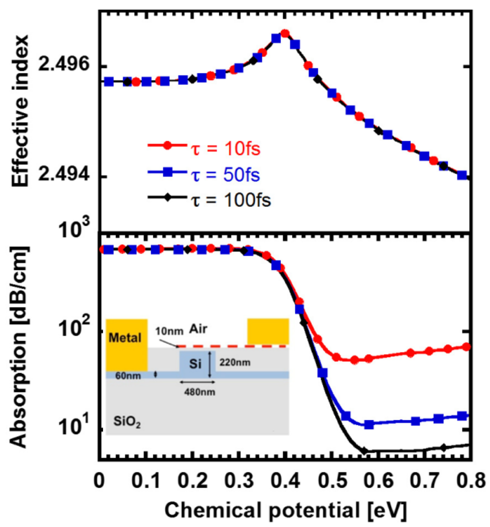
2.3. Graphene Electro-Refractive (ER) Modulator

The EA modulators reviewed above have shown remarkable performance in amplitude modulation. However, they do not have the ability to implement complex modulation formats (e.g., QAM) due to the lack of phase modulation, which is important for high-density long-haul communication. Since the E F can be controlled through gate voltage, the graphene-oxide-silicon (GOS)-based waveguide was found to be able to achieve either electro-absorptive or electro-refractive modulation. An MZI implemented with the graphene-oxide-silicon structure using the ER effect was proposed accordingly [65]. In the following years, many graphene ER modulator concepts were proposed and discussed.
The first experimental ER phase modulation was verified in 2015. The total refractive index change was relatively low and accompanied by absorption due to its low E f [66]. Later, the ER effect was experimentally characterized and induced a giant change in the effective index of around 10 3 in the GOS structure [46]. The first and most representative demonstration of data transmission utilizing the MZI-based ER modulator was reported in 2017. Two SLG sheets with a length difference (100 μm) were separately transferred onto the top of the two arms, which introduced a bias phase difference in the balanced MZI (Figure 6a). The device achieved the extinction ratio of 35 dB at static and a modulation efficiency of 0.28 V·cm. The bandwidth reached 5 GHz and open-eye diagram was observed at 10 Gbps, showing an error-free transmission over 50 kM SMF fibre (Figure 6b) [45]. Through the optimization of dielectric material in the capacitor, a better modulation efficiency of 0.129 V·cm was demonstrated with a 40-μm interaction length in the same year (Figure 6c) [67]. Their work paves the way for high-density integrated modulators, which are needed in high-capacity communication applications.
The DLG ER modulator was also demonstrated on Si 3 N 4 waveguide. A high- κ dielectric was embedded for large tuning of E f . When the graphene sheets were gated at the low loss region ( E F > 0.5 eV), a RF bandwidth of 0.64 GHz was obtained with a V π · L of 0.14 V·cm [68]. To achieve a high modulation efficiency, several ER modulations based on phase-manipulation waveguides were proposed. Based on the polarization multiplexing Mach–Zehnder Interferometer (PM-MZI), the light of different polarization states (TE and TM) passes through the modulation region four times, which allows for an order of magnitude enhancement of the modulation efficiency [69]. The MZI with two spiral arms was applied to decrease the footprint of the ER modulator while maintaining a high modulation efficiency [70]. Apart from the MZI structure, the GOS structure was integrated with a micro-ring structure. The ER effect was observed from the transmission spectra and the derived V π · L was 2.7 V·mm, which outperformed silicon depletion horizontal and interleaved p-n junction-type phase modulators (Figure 6d) [71].
Recently, the graphene-oxide-TMDs (GO-TMDs) hybrid, integrated with Si/Si 3 N 4 waveguide EO modulator, was demonstrated (Figure 6f–g) [72,73]. Since TMDs are transparent at near-IR wavelengths and can modulate the refractive index, when the gating voltage changes the loss in waveguide as well as the coupling state of microring through the graphene electro-absorption effect, the phase and resonance shift via modulating TMDs sheets. According to the spectra under different bias voltages, the calculated V π L is 1.5 V·cm in a graphene-oxide-WS 2 ER modulator based on silicon MZI (Figure 6f) [72]. For the graphene-MoS 2 on Si 3 N 4 micro-ring structure, an extinction of 30 dB across 20 V with an insertion loss of 5 dB was achieved (Figure 6g) [73].
Figure 6. Graphene ER modulators. (a,b) Optical micrograph and cross-section of the MZI-based graphene phase modulator with an electro-optical S21 bandwidth 5 GHz and an NRZ eye diagram at 10 Gbps [45]. Reproduced from Ref. [45] with permission. (c) TEM image for interaction region in graphene ER modulator based on MZI structure and static optical transmission with a great blue shift of about 185 pm under different applied voltages, indicating an ER modulation driven by graphene [67]. Reproduced from [67] with permission. (d) Micro-ring-based ER modulation covered by SLG. Inset shows SEM image with graphene visible and covering the ring resonator [71]. Reproduced from Ref. [71] with permission. (e) Optical micrograph and cross-section of the DLG-based (graphene-HfO 2 -graphene) ER modulator integrated on a Si 3 N 4 MZI structure. The optical transmission with an arm-length difference of 100 μm, indicating its ER modulation feature [68]. Reproduced from Ref. [68] with permission. (f) Left: schematic of the hybrid WS 2 -alumina-graphene modulator on passive silicon waveguide and the top-down microscope image of fabricated MZM device with 233 μm phase shifters. Transmission of the device under different bias conditions [72]. Reproduced from Ref. [72] with permission. (g) Diagrammatic of a MoS 2 -Al 2 O 3 -graphene capacitor placed on a Si 3 N 4 micro-ring. Experimentally measured normalized transmission for different voltages applied across monolayer graphene and MoS 2 [73]. Reproduced from Ref. [73] with permission.
Photonics 09 00082 g006

3. Potential Applications with Graphene EO Modulators

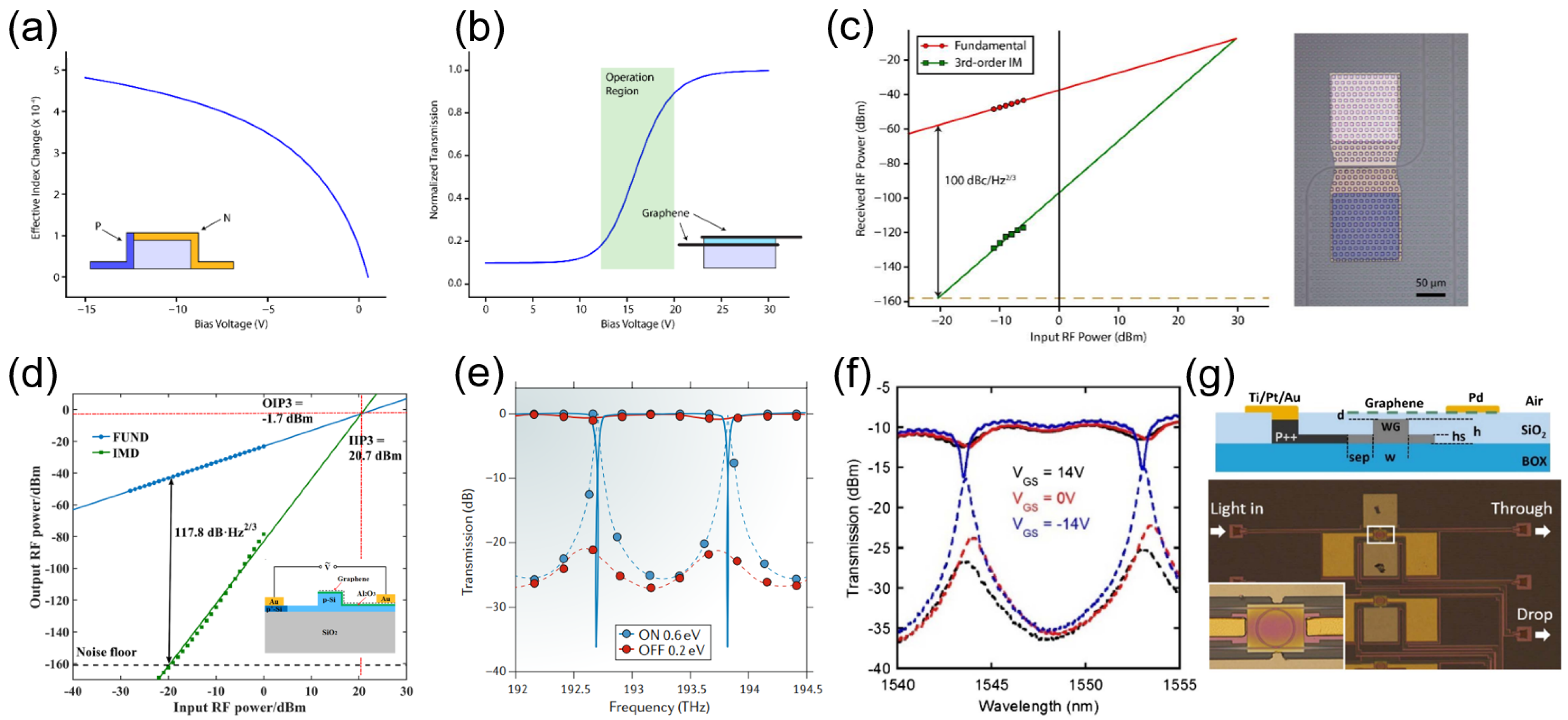
3.1. Optical Communications

With the advance in communications, the demand for modulators with high speed, large capacity and low energy consumption is increasing. Many graphene modulators with excellent performance have been demonstrated and exhibited enormous application potential in communication.
In order to meet the growing communication demand for large-capacity information modulation, people have begun to focus on the mass integration of graphene modulator arrays. In 2020, Chiara Alessandri et al. demonstrated a five-channel WDM transmitter consisting of five high-speed graphene EA modulators and a micro-ring with wave-division function, realizing multi-channel data transmission at 5 × 25 Gbps, as shown in Figure 7b [36]. Later, an integrated 32 graphene EA modulator was demonstrated on an 8 × 1 mm 2 chip. The performance deviation of devices was within 13%, and the averaged bandwidth was 3.9 GHz. The data rate was 7 Gbps; therefore, the total data transmission amount can reach 220 Gbps (Figure 7e) [42]. Moreover, the date rate is estimated to be greater than 0.6 Tbps through further optimization. The challenge of fabricating devices with a reliable performance at the wafer scale is overcome through optimization of all the manufacturing steps, including growth, transfer and fabrication protocols. In 2021, Macro et al. presented the full process of graphene optoelectronic devices’ flow at the wafer scale (Figure 7f) [33]. The mobility of the SLG sheet transferred to wafer demonstrated good quality (Figure 7g). Based on the flows, they fabricated 30 DLG EA modulators on Si 3 N 4 , achieving a maximum modulation rate of 20 Gbps. It is believed that, in the near future, the massive, low-cost production of graphene EO modulators and other graphene-based optoelectronic devices with uniform performance will meet more requirements for practical use.
In addition to the demands for the capacity and speed of communication, the quality of the transmitted signal is also crucial. After long-distance transmission, the optical signal will appear distorted because of the anomalous group velocity dispersion of SMF. Therefore, dispersion compensation and pre-chirp are the key steps to guarantee the quality of information transmission in fiber communication. Since the EO modulation in a graphene EA modulator can induce a large, positive linear chirp, the maximum shift in the instantaneous frequency reaches up to 1.8 GHz. By utilizing this property, the optical signal can be pre-chirped to compensate the effect of anomalous group velocity dispersion in fiber transmission. A 10 Gbps transmission on single-mode fiber with a temporal focusing distance (0-dB optical-signal-to-noise ratio (OSNR) penalty) of 60 km is demonstrated, and exceeds 100 km with a bit error rate (BER) that is largely lower than 10 3 (Figure 4b) [58]. To implement the practical use of the graphene EO modulator in the fiber-linked transmission network, a packaged graphene EA modulator was successfully demonstrated (Figure 4a) [58].
Signals generated by graphene EA modulators can be further improved by an optical pre-emphasis scheme using two cascaded modulators with different lengths [59]. The electrical signals that are applied to them are properly complemented for delay-inverse-weight compensation. As a result, a transmission of up to 100 km on single mode fiber (SMF) without dispersion compensation is reported, showing the advantage of the OSNR penalty (6 dB in back-to back and around 5 dB in transmission) compared with the conventional single EAM transmitter configuration (Figure 4d,e). Moreover, a highly efficient broadband fibre polarizer integrated with graphene has been proposed, which proves that graphene-based optoelectronic devices will play a more important role in optical fiber communication [74].
With the expansion of communication scenarios, the modulator is required to work under harsh conditions, which leads traditional modulators to face great challenges. Recent research has indicated that graphene modulators can maintain a stable performance in extreme environments. For example, the DLG EA modulator based on an amorphous Si waveguide can keep the RF response stable when the temperature reaches 145 C, which indicates a robust athermal operation (Figure 4f) [56]. A low temperature degrades the performance of the traditional silicon modulator due to the carrier freeze-out effect [20]. However, graphene has a higher mobility at low temperatures than it does at room temperature, which means that the graphene EO modulators can reach even higher modulation data rates (Figure 4g). Recently, the modulation features are explored at a cryogenic temperature. A DLG micro-ring modulator based on Si 3 N 4 waveguide obtained a 14.7 GHz bandwidth at 4.9 K (Figure 4h) [60]. These results indicate that the graphene-based EO modulators have great potential in communication applications under harsh conditions.
In conclusion, graphene modulators provide promising solutions to the problems in bandwidth rate, dispersion compensation and extreme conditions communication for future communication. It is believed that, with the maturity of wafer-level graphene-processing technology, various graphene modulators will be more widely used in different practical communication systems.

3.2. Microwave Photonics (MWP)

Along with the increasing demands for the capacity of wireless communications, MWP, processing a microwave signal by implementing the tremendous bandwidth of optics, is regarded as an indispensable technology for seamlessly interfacing between wireless and optical communication networks [75]. This technology has found use in satellite communication, phased array antennas, cellular networks, etc. Consequently, the integration of MWP (IMWP) systems using silicon photonics has been an essential solution to the challenges that arise from the complex application scenarios. However, the modulator, the most important building block of the IMWP system, faces the problems of a non-linear EO response and a large footprint due to the plasma-dispersion effect (Figure 8a) [76].
In practice, the modulation linearity is usually evaluated by the spurious free dynamic range (SFDR). In 2016, Christopher T. Phare et al. reported their characterization of the linearity of a graphene EA modulator [76]. Since the gradual transitions in absorption are governed by the Fermi–Dirac distribution of electrons in the bands, the accumulation change of the carrier on the graphene is linear with voltage. This transfer can occur across a wide range of bias voltage without explicit linearization techniques. A spurious free dynamic range (SFDR) of 100 dBc/Hz 2 / 3 was measured for the EA modulator with a GOG structure on Si 3 N 4 waveguide. Further linearity investigations of the graphene EO modualtor based on silicon waveguide were carried out by Yuansheng Tao et al. [77]. Through adjustments to the bias voltage of graphene, the maximum SFDR for IMD3 can reach 117.8 dBc/Hz 2 / 3 for the SLG EA modulator and 129.92 dBc/Hz 2 / 3 for the SLG ER modulator based on silicon waveguide. In addition, by using push–pull driving and quadrature biasing in the MZI graphene ER modulator, the SHD2 distortion can be fully eliminated. Note that, due to the tremendous mobility, the high linear waveguide graphene EO modulator can even be extended to the mm-wave frequency applications with a frequency exceeding 100 GHz. A recently demonstrated transmitter operating at 100 GHz based on a waveguide graphene optoelectronic mixer indicates this possibility [78].
Figure 8. Characterizations of graphene-based EO modulators towards MWP applications. (a) TCAD simulation for a silicon PN junction modulator. Inset: doping cross-section of the simulated modulator [76]. Reproduced from Ref. [76] with permission. (b) Calculated transmission versus bias voltage for a graphene EA modulator. Inset: modulator cross-section applying GOG capacitor [76]. (c) Two-tone (centered at 2.5 GHz) intermodulation response of the GOG EA modulator based on Si 3 N 4 waveguide. Inset: optical microscope image of the tested device [76]. (d) Calculated maximal SFDR for IMD3 obtained for the SLG EA modulator based on Si with an optimized insulation layer. Inset: schematic of the graphene EA modulator [77]. Reproduced from Ref. [77] with permission. (e) Calculated transmission spectra as a function of frequency for a Si micro-ring resonator in the ON (minimum micro-ring resonator absorption at E f = 0.6 eV) and OFF states (maximum micro-ring resonator absorption) [79]. Reproduced from Ref. [79] with permission. (f) Experimental through (solid lines) and drop (dashed lines) transmission spectra of GOS MRR switch for different gate voltage values. (g) Cross-section of the GOS waveguide and the optical micrograph picture of fabricated devices [80]. Reproduced from Ref. [80] with permission.
Photonics 09 00082 g008
For next-generation wireless networks, the massive beam forming at the mm wave spectrum requires a high link bandwidth as well as the responsiveness (>MHz). Thus, optical switching is crucial for fully MWP systems. For the optical switch based on an add-drop micro-ring, a thermo-optic effect is applied to shift the resonant frequency in conventional method, whereas the SLG-based optical switch enables the on/off state by suppressing the resonator resonance through a capacitor. As a consequence, the energy is only consumed during capacitance charging, which is much more power-efficient than metal heating. In addition, the SLG switch has a much lower response time and crosstalk in switching than that based on thermo-optic modulation [79,80].

4. Challenges and Outlook

Taking advantage of the unique properties of the gapless semimetallic band structure, the fast tuning of the surface conductivity and the compatible nature with a SiPh platform, graphene-based optoelectronics devices have made substantial progress in almost all aspects—including design, fabrication, measurement, and applications—which lead to disruptive development for next-generation photonics. In this review, we discuss the development of silicon-based graphene EO modulators over the last decade (the typical performance is summarized in Table 1). It has been shown that research interest is shifting from the proof-of-concept demonstrations to advance technologies for practical applications. With the attempts in certain scenarios, challenges are emerging.
To integrate graphene with the current CMOS technology, several challenges should be noted in terms of manufacturing process, device stability, cost and production yield. Firstly, a highly reliable transfer method of SLG to silicon chip is required to maintain high mobility, coverage and continuity. The wet-transfer method is the most widespread and easy method, through which the mobility is limited at about 10 3 cm 2 V 1 s 1 . The fully dry method can transfer SLG without contact with water or solvents, resulting in a mobility of up to 3 × 10 5 cm 2 V 1 s 1 . However, the scalability is limited by the size (∼100 μm) of hBN flakes or other layered materials used to pick-up SLG from Cu. An aligned semi-dry SLG transfer, based on electrochemical delamination and the subsequent handling of a suspended polymer/SLG membrane, can realize an average mobility of about 5000 cm 2 V 1 s 1 , while covering 80% of a die [33]. At present, these methods cannot be directly applied to a standard wafer-scale CMOS process due to their scalability. Secondly, the device stability, especially the hysteresis phenomenon, should be improved by encapsulation. h-BN flakes are the most common material used to encapsulate the SLG, but are difficult to introduce to the CMOS process due to the size limitation of exfoliated flakes. A more feasible method, allowing large scalability to protect SLG, is challenging and strongly desired. Thirdly, the cost and production yield of graphene-based devices should be increased through optimization in terms of SLG continuity or the deterministic placement of SLG. In fact, the interaction region of graphene-based device can be relatively smaller, and most of the transferred graphene sheets are wasted after pattering. Thus, a high-precision pattering and transferring technology can greatly decrease the waste of graphene to reduce costs and increase yields.
Although the modulation types can be switched via gating, the ER modulation is hard to reach because the dielectric inside the capacitor structure is very likely to be permanently damaged when graphene approaches the Pauli blocking state. Thus, the graphene EA modulator is studied more extensively. At present, the highest transmission rate for graphene EA and ER modulators is up to 50 Gbps and 10 Gbps, respectively. For short-distance interconnects, e.g., in the datacenter, the waveguide EA modulator can be an excellent choice to replace the silicon-based modulator in the transmitter due to its compact footprint (length ∼100 μm) and broadband response. To achieve high-spectral-density communication channels and maximize the spectral efficiency during long-haul and parallel optical communications, a phase modulator must be employed to realize complex modulation formats. However, to date, only one group succeeded in demonstrating the graphene ER modulator operating at a speed exceeding 1 Gbps, which still works in an on–off keying format. No transmission link based on phase-shift keying modulation format has been demonstrated, and this remains to be explored. A packaged version of a single modulator with input and output fibers mounted on a dedicated PCB has been reported. To deploy the Graphene EO modulator in real applications, a multi-channel optical and electrical packaging method with long-term stability is required. The graphene EA modulators with encapsulated graphene monolayer were proved to have an enhanced performance and uniform stability, which should be promoted.
Since the graphene monolayer can realize both the EO modulation and photodetection, in complex applications based on a photonic circuit involving more than one active device, a graphene-based system needs both modulators and photodetectors simultaneously. Hindered by the limited light–matter interaction, high-performance graphene-based photodetector is always assisted by special photonic configurations, for example, SPPs and thin waveguide. Thus, it is vital as well as challenging to develop a more versatile fabrication process that can satisfy the different requirements. In addition, the graphene EO modulator has shown speed stability in a wide range of temperatures (25–145 C). The EO bandwidth at cryogenic temperature is even higher than that at room temperature, while the conventional silicon modulator suffering from the carrier freeze-out effect can barely work. These facts make it a promising candidate in harsh environmental applications, for example, solid-state quantum computing, intersatellite optical communications or superconducting tests. The graphene ER modulation is further used to control the nonlinear effects in microresonators. The gate-tunable Fermi energy induces changes in the primary comb lines offset, coherent Kerr frequency combs, controllable Cherenkov radiation and controllable soliton states. It is believed that a silicon-based graphene EO modulator will continue to develop rapidly, enabling further applications.

Author Contributions

Writing—original draft preparation, M.J., Z.W. and Y.M.; writing—review and editing, M.J., Z.W., Y.M., H.S., B.B., Y.T. and X.W.; supervision, X.W. All authors have read and agreed to the published version of the manuscript.

Funding

This work was supported by National Key R&D Program of China (Grant No. 2021YFB 2800400), Beijing Natural Science Foundation (Z210004), National Natural Science Foundation of China (Grant No. 62105008, 61635001, 62001010), China Postdoctoral Science Foundation (Grant No. 2021T140004, 2021M700259), China National Postdoctoral Program for Innovative Talents (BX20200017).

Institutional Review Board Statement

Not applicable.

Informed Consent Statement

Not applicable.

Acknowledgments

The authors thank J. Qin for helpful discussions.

Conflicts of Interest

The authors declare no conflict of interest.

References

  1. Cisco Annual Internet Report (2018–2023) White Paper. Available online: https://www.cisco.com/c/en/us/solutions/collateral/executive-perspectives/annual-internet-report/white-paper-c11-741490.html (accessed on 28 December 2021).
  2. IDC. Global ICT Spending-forecast 2020–2023. Available online: https://www.idc.com/promo/global-ict-spending/forecast (accessed on 28 December 2021).
  3. Thomson, D.; Zilkie, A.; Bowers, J.E.; Komljenovic, T.; Reed, G.T.; Vivien, L.; Marris-Morini, D.; Cassan, E.; Virot, L.; Fédéli, J.M.; et al. Roadmap on silicon photonics. J. Opt. 2016, 18, 073003. [Google Scholar] [CrossRef]
  4. Shu, H.; Chang, L.; Tao, Y.; Shen, B.; Xie, W.; Jin, M.; Netherton, A.; Tao, Z.; Zhang, X.; Chen, R. Bridging microcombs and silicon photonic engines for optoelectronics systems. arXiv 2021, arXiv:2110.12856. [Google Scholar]
  5. Pelucchi, E.; Fagas, G.; Aharonovich, I.; Englund, D.; Figueroa, E.; Gong, Q.; Hannes, H.; Liu, J.; Lu, C.Y.; Matsuda, N.; et al. The potential and global outlook of integrated photonics for quantum technologies. Nat. Rev. Phys. 2021. [Google Scholar] [CrossRef]
  6. Westerveld, W.J.; Mahmud-Ul-Hasan, M.; Shnaiderman, R.; Ntziachristos, V.; Rottenberg, X.; Severi, S.; Rochus, V. Sensitive, small, broadband and scalable optomechanical ultrasound sensor in silicon photonics. Nat. Photonics 2021, 15, 341–345. [Google Scholar] [CrossRef]
  7. Tasker, J.F.; Frazer, J.; Ferranti, G.; Allen, E.J.; Brunel, L.F.; Tanzilli, S.; D’Auria, V.; Matthews, J.C.F. Silicon photonics interfaced with integrated electronics for 9 GHz measurement of squeezed light. Nat. Photonics 2021, 15, 11–15. [Google Scholar] [CrossRef]
  8. Rogers, C.; Piggott, A.Y.; Thomson, D.J.; Wiser, R.F.; Opris, I.E.; Fortune, S.A.; Compston, A.J.; Gondarenko, A.; Meng, F.; Chen, X.; et al. A universal 3D imaging sensor on a silicon photonics platform. Nature 2021, 590, 256–261. [Google Scholar] [CrossRef]
  9. Datta, I.; Chae, S.H.; Bhatt, G.R.; Tadayon, M.A.; Li, B.; Yu, Y.; Park, C.; Park, J.; Cao, L.; Basov, D.N.; et al. Low-loss composite photonic platform based on 2D semiconductor monolayers. Nat. Photonics 2020, 14, 256–262. [Google Scholar] [CrossRef]
  10. Chang, L.; Xie, W.; Shu, H.; Yang, Q.F.; Shen, B.; Boes, A.; Peters, J.D.; Jin, W.; Xiang, C.; Liu, S.; et al. Ultra-efficient frequency comb generation in AlGaAs-on-insulator microresonators. Nat. Commun. 2020, 11, 1331. [Google Scholar] [CrossRef]
  11. Idjadi, M.H.; Aflatouni, F. Nanophotonic phase noise filter in silicon. Nat. Photonics 2020, 14, 234–239. [Google Scholar] [CrossRef]
  12. Huang, C.; Fujisawa, S.; de Lima, T.F.; Tait, A.N.; Blow, E.C.; Tian, Y.; Bilodeau, S.; Jha, A.; Yaman, F.; Peng, H.T.; et al. A silicon photonic–electronic neural network for fibre nonlinearity compensation. Nat. Electron. 2021, 4, 837–844. [Google Scholar] [CrossRef]
  13. Ummethala, S.; Harter, T.; Koehnle, K.; Li, Z.; Muehlbrandt, S.; Kutuvantavida, Y.; Kemal, J.; Marin-Palomo, P.; Schaefer, J.; Tessmann, A.; et al. THz-to-optical conversion in wireless communications using an ultra-broadband plasmonic modulator. Nat. Photonics 2019, 13, 519–524. [Google Scholar] [CrossRef]
  14. Reed, G.T.; Mashanovich, G.; Gardes, F.Y.; Thomson, D.J. Silicon optical modulators. Nat. Photonics 2010, 4, 518–526. [Google Scholar] [CrossRef] [Green Version]
  15. Xu, Q.; Schmidt, B.; Pradhan, S.; Lipson, M. Micrometre-scale silicon electro-optic modulator. Nature 2005, 435, 325–327. [Google Scholar] [CrossRef] [PubMed]
  16. Rahim, A.; Goyvaerts, J.; Szelag, B.; Fedeli, J.M.; Absil, P.; Aalto, T.; Harjanne, M.; Littlejohns, C.; Reed, G.; Winzer, G.; et al. Open-Access Silicon Photonics Platforms in Europe. IEEE J. Sel. Top. Quantum Electron. 2019, 25, 1–18. [Google Scholar] [CrossRef] [Green Version]
  17. Timurdogan, E.; Su, Z.; Poulton, C.V.; Byrd, M.J.; Xin, S.; Shiue, R.J.; Moss, B.R.; Hosseini, E.S.; Watts, M.R. AIM Process Design Kit (AIMPDKv2.0): Silicon Photonics Passive and Active Component Libraries on a 300 mm Wafer. In Proceedings of the Optical Fiber Communication Conference 2018, San Diego, CA, USA, 11–15 March 2018. [Google Scholar] [CrossRef]
  18. Haffner, C.; Chelladurai, D.; Fedoryshyn, Y.; Josten, A.; Baeuerle, B.; Heni, W.; Watanabe, T.; Cui, T.; Cheng, B.; Saha, S.; et al. Low-loss plasmon-assisted electro-optic modulator. Nature 2018, 556, 483–486. [Google Scholar] [CrossRef]
  19. Eltes, F.; Villarreal-Garcia, G.E.; Caimi, D.; Siegwart, H.; Gentile, A.A.; Hart, A.; Stark, P.; Marshall, G.D.; Thompson, M.G.; Barreto, J.; et al. An integrated optical modulator operating at cryogenic temperatures. Nat. Mater. 2020, 19, 1164–1168. [Google Scholar] [CrossRef]
  20. Gehl, M.; Long, C.; Trotter, D.; Starbuck, A.; Pomerene, A.; Wright, J.B.; Melgaard, S.; Siirola, J.; Lentine, A.L.; DeRose, C. Operation of high-speed silicon photonic micro-disk modulators at cryogenic temperatures. Optica 2017, 4, 374–382. [Google Scholar] [CrossRef]
  21. Dong, M.; Clark, G.; Leenheer, A.J.; Zimmermann, M.; Dominguez, D.; Menssen, A.J.; Heim, D.; Gilbert, G.; Englund, D.; Eichenfield, M. High-speed programmable photonic circuits in a cryogenically compatible, visible–near-infrared 200 mm CMOS architecture. Nat. Photonics 2022, 16, 59–65. [Google Scholar] [CrossRef]
  22. He, M.; Xu, M.; Ren, Y.; Jian, J.; Ruan, Z.; Xu, Y.; Gao, S.; Sun, S.; Wen, X.; Zhou, L.; et al. High-performance hybrid silicon and lithium niobate Mach–Zehnder modulators for 100 Gbit·s−1 and beyond. Nat. Photonics 2019, 13, 359–364. [Google Scholar] [CrossRef]
  23. Wang, C.; Zhang, M.; Chen, X.; Bertrand, M.; Shams-Ansari, A.; Chandrasekhar, S.; Winzer, P.; Lončar, M. Integrated lithium niobate electro-optic modulators operating at CMOS-compatible voltages. Nature 2018, 562, 101–104. [Google Scholar] [CrossRef]
  24. Lu, G.W.; Hong, J.; Qiu, F.; Spring, A.M.; Kashino, T.; Oshima, J.; Ozawa, M.a.; Nawata, H.; Yokoyama, S. High-temperature-resistant silicon-polymer hybrid modulator operating at up to 200 Gbit·s−1 for energy-efficient datacentres and harsh-environment applications. Nat. Commun. 2020, 11, 4224. [Google Scholar] [CrossRef]
  25. Hiraki, T.; Aihara, T.; Hasebe, K.; Takeda, K.; Fujii, T.; Kakitsuka, T.; Tsuchizawa, T.; Fukuda, H.; Matsuo, S. Heterogeneously integrated III–V/Si MOS capacitor Mach–Zehnder modulator. Nat. Photonics 2017, 11, 482–485. [Google Scholar] [CrossRef]
  26. Liu, M.; Yin, X.; Ulin-Avila, E.; Geng, B.; Zentgraf, T.; Ju, L.; Wang, F.; Zhang, X. A graphene-based broadband optical modulator. Nature 2011, 474, 64–67. [Google Scholar] [CrossRef] [PubMed]
  27. Phare, C.T.; Daniel Lee, Y.H.; Cardenas, J.; Lipson, M. Graphene electro-optic modulator with 30 GHz bandwidth. Nat. Photonics 2015, 9, 511–514. [Google Scholar] [CrossRef]
  28. Liu, C.; Chen, H.; Wang, S.; Liu, Q.; Jiang, Y.G.; Zhang, D.W.; Liu, M.; Zhou, P. Two-dimensional materials for next-generation computing technologies. Nat. Nanotechnol. 2020, 15, 545–557. [Google Scholar] [CrossRef] [PubMed]
  29. Haffner, C.; Heni, W.; Fedoryshyn, Y.; Niegemann, J.; Melikyan, A.; Elder, D.L.; Baeuerle, B.; Salamin, Y.; Josten, A.; Koch, U.; et al. All-plasmonic Mach–Zehnder modulator enabling optical high-speed communication at the microscale. Nat. Photonics 2015, 9, 525–528. [Google Scholar] [CrossRef]
  30. Goossens, S.; Navickaite, G.; Monasterio, C.; Gupta, S.; Piqueras, J.J.; Pérez, R.; Burwell, G.; Nikitskiy, I.; Lasanta, T.; Galán, T.; et al. Broadband image sensor array based on graphene–CMOS integration. Nat. Photonics 2017, 11, 366–371. [Google Scholar] [CrossRef]
  31. Neumaier, D.; Pindl, S.; Lemme, M.C. Integrating graphene into semiconductor fabrication lines. Nat. Mater. 2019, 18, 525–529. [Google Scholar] [CrossRef] [PubMed] [Green Version]
  32. Cheng, Z.; Zhu, X.; Galili, M.; Frandsen, L.H.; Hu, H.; Xiao, S.; Dong, J.; Ding, Y.; Oxenløwe, L.K.; Zhang, X. Double-layer graphene on photonic crystal waveguide electro-absorption modulator with 12 GHz bandwidth. Nanophotonics 2020, 9, 2377–2385. [Google Scholar] [CrossRef]
  33. Giambra, M.A.; Mišeikis, V.; Pezzini, S.; Marconi, S.; Montanaro, A.; Fabbri, F.; Sorianello, V.; Ferrari, A.C.; Coletti, C.; Romagnoli, M. Wafer-Scale Integration of Graphene-Based Photonic Devices. ACS Nano 2021, 15, 3171–3187. [Google Scholar] [CrossRef]
  34. Liu, M.; Yin, X.; Zhang, X. Double-Layer Graphene Optical Modulator. Nano Lett. 2012, 12, 1482–1485. [Google Scholar] [CrossRef] [PubMed]
  35. Agarwal, H.; Terrés, B.; Orsini, L.; Montanaro, A.; Sorianello, V.; Pantouvaki, M.; Watanabe, K.; Taniguchi, T.; Thourhout, D.V.; Romagnoli, M.; et al. 2D-3D integration of hexagonal boron nitride and a high-κ dielectric for ultrafast graphene-based electro-absorption modulators. Nat. Commun. 2021, 12, 1070. [Google Scholar] [CrossRef] [PubMed]
  36. Alessandri, C.; Asselberghs, I.; Brems, S.; Huyghebaert, C.; Van Campenhout, J.; Van Thourhout, D.; Pantouvaki, M. 5 × 25 Gbit/s WDM transmitters based on passivated graphene-silicon electro-absorption modulators. Appl. Opt. 2020, 59, 1156–1162. [Google Scholar] [CrossRef]
  37. Sun, Z.; Chang, H. Graphene and Graphene-like Two-Dimensional Materials in Photodetection: Mechanisms and Methodology. ACS Nano 2014, 8, 4133–4156. [Google Scholar] [CrossRef] [PubMed]
  38. Marconi, S.; Giambra, M.A.; Montanaro, A.; Mišeikis, V.; Soresi, S.; Tirelli, S.; Galli, P.; Buchali, F.; Templ, W.; Coletti, C.; et al. Photo thermal effect graphene detector featuring 105 Gbit·s−1 NRZ and 120 Gbit·s−1 PAM4 direct detection. Nat. Commun. 2021, 12, 806. [Google Scholar] [CrossRef] [PubMed]
  39. Schuler, S.; Muench, J.E.; Ruocco, A.; Balci, O.; Thourhout, D.v.; Sorianello, V.; Romagnoli, M.; Watanabe, K.; Taniguchi, T.; Goykhman, I.; et al. High-responsivity graphene photodetectors integrated on silicon microring resonators. Nat. Commun. 2021, 12, 3733. [Google Scholar] [CrossRef] [PubMed]
  40. Wang, Y.; Li, X.; Jiang, Z.; Tong, L.; Deng, W.; Gao, X.; Huang, X.; Zhou, H.; Yu, Y.; Ye, L.; et al. Ultrahigh-speed graphene-based optical coherent receiver. Nat. Commun. 2021, 12, 5076. [Google Scholar] [CrossRef]
  41. Guo, J.; Li, J.; Liu, C.; Yin, Y.; Wang, W.; Ni, Z.; Fu, Z.; Yu, H.; Xu, Y.; Shi, Y.; et al. High-performance silicon-graphene hybrid plasmonic waveguide photodetectors beyond 1.55 μm. Light. Sci. Appl. 2020, 9, 29. [Google Scholar] [CrossRef] [Green Version]
  42. Lee, B.S.; Freitas, A.P.; Gil-Molina, A.; Shim, E.; Zhu, Y.; Hone, J.; Lipson, M. Scalable graphene platform for Tbits/s data transmission. arXiv 2020, arXiv:2011.08832. [Google Scholar]
  43. Mak, K.F.; Ju, L.; Wang, F.; Heinz, T.F. Optical spectroscopy of graphene: From the far infrared to the ultraviolet. Solid State Commun. 2012, 152, 1341–1349. [Google Scholar] [CrossRef]
  44. Rouhi, N.; Capdevila, S.; Jain, D.; Zand, K.; Wang, Y.Y.; Brown, E.; Jofre, L.; Burke, P. Terahertz graphene optics. Nano Res. 2012, 5, 667–678. [Google Scholar] [CrossRef]
  45. Sorianello, V.; Midrio, M.; Contestabile, G.; Asselberghs, I.; Van Campenhout, J.; Huyghebaert, C.; Goykhman, I.; Ott, A.K.; Ferrari, A.C.; Romagnoli, M. Graphene-silicon phase modulators with gigahertz bandwidth. Nat. Photonics 2018, 12, 40–44. [Google Scholar] [CrossRef]
  46. Sorianello, V.; De Angelis, G.; Cassese, T.; Midrio, M.; Romagnoli, M.; Mohsin, M.; Otto, M.; Neumaier, D.; Asselberghs, I.; Van Campenhout, J.; et al. Complex effective index in graphene-silicon waveguides. Opt. Express 2016, 24, 29984–29993. [Google Scholar] [CrossRef] [PubMed]
  47. Chang, Y.C.; Liu, C.H.; Liu, C.H.; Zhong, Z.; Norris, T.B. Extracting the complex optical conductivity of mono- and bilayer graphene by ellipsometry. Appl. Phys. Lett. 2014, 104, 261909. [Google Scholar] [CrossRef] [Green Version]
  48. Chang, Z.; Chiang, K.S. Experimental verification of optical models of graphene with multimode slab waveguides. Opt. Lett. 2016, 41, 2129–2132. [Google Scholar] [CrossRef]
  49. Lao, J.; Tao, J.; Wang, Q.J.; Huang, X.G. Tunable graphene-based plasmonic waveguides: Nano modulators and nano attenuators. Laser Photonics Rev. 2014, 8, 569–574. [Google Scholar] [CrossRef]
  50. Sorianello, V.; Midrio, M.; Romagnoli, M. Design optimization of single and double layer Graphene phase modulators in SOI. Opt. Express 2015, 23, 6478–6490. [Google Scholar] [CrossRef]
  51. Hu, Y.; Pantouvaki, M.; Van Campenhout, J.; Brems, S.; Asselberghs, I.; Huyghebaert, C.; Absil, P.; Van Thourhout, D. Broadband 10 Gb/s operation of graphene electro-absorption modulator on silicon. Laser Photonics Rev. 2016, 10, 307–316. [Google Scholar] [CrossRef] [Green Version]
  52. Alessandri, C.; Asselberghs, I.; Brems, S.; Huyghebaert, C.; Van Campenhout, J.; Van Thourhout, D.; Pantouvaki, M. High speed single-layer graphene-Si electro-absorption modulator. In Proceedings of the Conference on Lasers and Electro-Optics/Pacific Rim 2018, Hong Kong, China, 29 July–3 August 2018. [Google Scholar] [CrossRef]
  53. Alessandri, C.; Asselberghs, I.; Brems, S.; Huyghebaert, C.; Van Campenhout, J.; Van Thourhout, D.; Pantouvaki, M. High speed graphene-silicon electro-absorption modulators for the O-band and C-band. Jpn. J. Appl. Phys. 2020, 59, 052008. [Google Scholar] [CrossRef]
  54. Mohsin, M.; Schall, D.; Otto, M.; Noculak, A.; Neumaier, D.; Kurz, H. Graphene based low insertion loss electro-absorption modulator on SOI waveguide. Opt. Express 2014, 22, 15292–15297. [Google Scholar] [CrossRef]
  55. Youngblood, N.; Anugrah, Y.; Ma, R.; Koester, S.J.; Li, M. Multifunctional Graphene Optical Modulator and Photodetector Integrated on Silicon Waveguides. Nano Lett. 2014, 14, 2741–2746. [Google Scholar] [CrossRef] [PubMed] [Green Version]
  56. Dalir, H.; Xia, Y.; Wang, Y.; Zhang, X. Athermal Broadband Graphene Optical Modulator with 35 GHz Speed. ACS Photonics 2016, 3, 1564–1568. [Google Scholar] [CrossRef]
  57. Giambra, M.A.; Sorianello, V.; Miseikis, V.; Marconi, S.; Montanaro, A.; Galli, P.; Pezzini, S.; Coletti, C.; Romagnoli, M. High-speed double layer graphene electro-absorption modulator on SOI waveguide. Opt. Express 2019, 27, 20145–20155. [Google Scholar] [CrossRef]
  58. Sorianello, V.; Contestabile, G.; Midrio, M.; Pantouvaki, M.; Asselbergs, I.; Van Campenhout, J.; Huyghebaerts, C.; D’Errico, A.; Galli, P.; Romagnoli, M. Chirp management in silicon-graphene electro absorption modulators. Opt. Express 2017, 25, 19371–19381. [Google Scholar] [CrossRef] [Green Version]
  59. Sorianello, V.; Contestabile, G.; Midrio, M.; Pantouvaki, M.; Asselbergs, I.; Campenhout, J.V.; Huyghebaerts, C.; Romagnoli, M. Optical Pre-Emphasis by Cascaded Graphene Electro Absorption Modulators. IEEE Photonics Technol. Lett. 2019, 31, 955–958. [Google Scholar] [CrossRef]
  60. Lee, B.S.; Kim, B.; Freitas, A.P.; Mohanty, A.; Zhu, Y.; Bhatt, G.R.; Hone, J.; Lipson, M. High-performance integrated graphene electro-optic modulator at cryogenic temperature. Nanophotonics 2021, 10, 99–104. [Google Scholar] [CrossRef]
  61. Qiu, C.; Gao, W.; Vajtai, R.; Ajayan, P.M.; Kono, J.; Xu, Q. Efficient Modulation of 1.55 μm Radiation with Gated Graphene on a Silicon Microring Resonator. Nano Lett. 2014, 14, 6811–6815. [Google Scholar] [CrossRef] [Green Version]
  62. Ding, Y.; Zhu, X.; Xiao, S.; Hu, H.; Frandsen, L.H.; Mortensen, N.A.; Yvind, K. Effective Electro-Optical Modulation with High Extinction Ratio by a Graphene–Silicon Microring Resonator. Nano Lett. 2015, 15, 4393–4400. [Google Scholar] [CrossRef] [Green Version]
  63. Ansell, D.; Radko, I.P.; Han, Z.; Rodriguez, F.J.; Bozhevolnyi, S.I.; Grigorenko, A.N. Hybrid graphene plasmonic waveguide modulators. Nat. Commun. 2015, 6, 8846. [Google Scholar] [CrossRef]
  64. Ding, Y.; Guan, X.; Zhu, X.; Hu, H.; Bozhevolnyi, S.I.; Oxenløwe, L.K.; Jin, K.J.; Mortensen, N.A.; Xiao, S. Efficient electro-optic modulation in low-loss graphene-plasmonic slot waveguides. Nanoscale 2017, 9, 15576–15581. [Google Scholar] [CrossRef] [Green Version]
  65. Hao, R.; Du, W.; Chen, H.; Jin, X.; Yang, L.; Li, E. Ultra-compact optical modulator by graphene induced electro-refraction effect. Appl. Phys. Lett. 2013, 103, 061116. [Google Scholar] [CrossRef]
  66. Mohsin, M.; Neumaier, D.; Schall, D.; Otto, M.; Matheisen, C.; Lena Giesecke, A.; Sagade, A.A.; Kurz, H. Experimental verification of electro-refractive phase modulation in graphene. Sci. Rep. 2015, 5, 10967. [Google Scholar] [CrossRef] [PubMed] [Green Version]
  67. Shu, H.; Su, Z.; Huang, L.; Wu, Z.; Wang, X.; Zhang, Z.; Zhou, Z. Significantly High Modulation Efficiency of Compact Graphene Modulator Based on Silicon Waveguide. Sci. Rep. 2018, 8, 991. [Google Scholar] [CrossRef] [PubMed]
  68. Datta, I.; Phare, C.T.; Dutt, A.; Mohanty, A.; Lipson, M. Integrated Graphene Electro-Optic Phase Modulator. In Proceedings of the CLEO: Science and Innovations 2017, San Jose, CA, USA, 14–19 May 2017. [Google Scholar] [CrossRef]
  69. Shu, H.; Deng, Q.; Jin, M.; Tao, Y.; Wang, X.; Zhou, Z. Efficient Graphene Phase Modulator Based on a Polarization Multiplexing Optical Circuit. In Proceedings of the 2019 Optical Fiber Communications Conference and Exhibition (OFC), San Diego, CA, USA, 3–7 March 2019; pp. 1–3. [Google Scholar]
  70. Shu, H.; Wu, Z.; Li, Y.; Wang, X.; Li, Y.; Zhou, Z. High Efficiency Graphene Phase Modulator Based on Silicon Spiral Waveguide. In Proceedings of the Asia Communications and Photonics Conference 2017, Guangzhou, China, 10–13 November 2017. [Google Scholar] [CrossRef]
  71. Mohsin, M.; Schall, D.; Otto, M.; Chmielak, B.; Suckow, S.; Neumaier, D. Towards the Predicted High Performance of Waveguide Integrated Electro-Refractive Phase Modulators Based on Graphene. IEEE Photonics J. 2017, 9, 1–7. [Google Scholar] [CrossRef]
  72. Wu, C.; Brems, S.; Asselberghs, I.; Huyghebaert, C.; Sorianello, V.; Romagnoli, M.; Van Campenhout, J.; Van Thourhout, D.; Pantouvaki, M. Hybrid Graphene-WS2 Mach-Zehnder modulator on passive silicon waveguide. In Proceedings of the 2021 Conference on Lasers and Electro-Optics Europe and European Quantum Electronics Conference, Virtual, Munich, Germany, 21–25 June 2021. [Google Scholar]
  73. Datta, I.; Jimenez Gordillo, O.A.; Chae, S.H.; Hone, J.; Lipson, M. Platform for electrically reconfigurable ring resonator based on TMD-graphene composite waveguides. In Proceedings of the CLEO: Science and Innovations 2021, San Jose, CA, USA, 9–14 May 2021. [Google Scholar] [CrossRef]
  74. Bao, Q.; Zhang, H.; Wang, B.; Ni, Z.; Lim, C.H.Y.X.; Wang, Y.; Tang, D.Y.; Loh, K.P. Broadband graphene polarizer. Nat. Photonics 2011, 5, 411–415. [Google Scholar] [CrossRef]
  75. Fandiño, J.S.; Muñoz, P.; Doménech, D.; Capmany, J. A monolithic integrated photonic microwave filter. Nat. Photonics 2017, 11, 124–129. [Google Scholar] [CrossRef] [Green Version]
  76. Phare, C.T.; Cardenas, J.; Lee, Y.H.D.; Lipson, M. Linear Graphene on Silicon Nitride Electroabsorption Modulators for RF-Over-Fiber Links. In Proceedings of the CLEO: Science and Innovations 2016, San Jose, CA, USA, 5–10 June 2016. [Google Scholar] [CrossRef]
  77. Tao, Y.; Shu, H.; Jin, M.; Wang, X.; Zhou, L.; Zou, W. Numerical investigation of the linearity of graphene-based silicon waveguide modulator. Opt. Express 2019, 27, 9013–9031. [Google Scholar] [CrossRef]
  78. Montanaro, A.; Sorianello, V.; Giambra, M.A.; Mišeikis, V.; Pezzini, S.; Giorgi, L.; D’Errico, A.; Bigongiari, A.; Cavaliere, F.; Coletti, C.; et al. Optically enabled graphene-based transmitter for Gbit/s links at 93 GHz carrier frequency. In Proceedings of the Photonics in Switching and Computing 2021, Washington, DC, USA, 27–29 September 2021. [Google Scholar]
  79. Romagnoli, M.; Sorianello, V.; Midrio, M.; Koppens, F.H.L.; Huyghebaert, C.; Neumaier, D.; Galli, P.; Templ, W.; D’Errico, A.; Ferrari, A.C. Graphene-based integrated photonics for next-generation datacom and telecom. Nat. Rev. Mater. 2018, 3, 392–414. [Google Scholar] [CrossRef] [Green Version]
  80. Cassese, T.; Giambra, M.A.; Sorianello, V.; De Angelis, G.; Midrio, M.; Pantouvaki, M.; Van Campenhout, J.; Asselberghs, I.; Huyghebaert, C.; D’Errico, A.; et al. Capacitive actuation and switching of add-drop graphene-silicon micro-ring filters. Photonics Res. 2017, 5, 762–766. [Google Scholar] [CrossRef] [Green Version]
Figure 1. Effective index (top) and absorption (bottom) of the graphene-integrated Si waveguide at 1.55 μm versus chemical potential in graphene, the intra-band relaxation time τ represent different graphene qualities. Inset: the cross-section of silicon-based graphene waveguide used in calculations [46]. Reproduced from [46] with permission.
Photonics 09 00082 g001
Figure 2. SLG−based EA modulator. (a) Left: a three-dimensional, schematic illustration of the first silicon-based SLG EA modulator. Right: the EO frequency response of the deviceunder different-drive voltage [26]. Reproduced from Ref. [26] with permission. (b) 3D schematic drawing of a single-layer graphene EA modulator (EAM) integrated on silicon waveguide with a flat surface. Measured S21 responses and optical eye diagrams (modulation speed: 8 Gbps and 10 Gbps) of the 50 μm graphene EAM at different bias voltages [51]. Reproduced from Ref. [51] with permission. (c) Schematic cross-section of the graphene EAM indicating the equivalent electrical model and measured 3 dB-bandwidth up to 17.6 GHz for a 25 μm-long p-Si device at 0 V, 1 V and 2 V [52]. Reproduced from Ref. [52] with permission. (d) Schematic 3D structure of the graphene-Si EA modulator with a encapsulate graphene through the passivation-first approach. Measured eye diagrams operating at 25 Gbps [36]. Reproduced from Ref. [36] with permission.
Photonics 09 00082 g002
Figure 3. DLG−based EA modulator. (a) EO response of the DLG modulator with a 3 dB-bandwidth of ∼1 GHz. Inset: the corresponding structure of the first silicon-based DLG modulator device [34]. Reproduced from Ref. [34] with permission. (b) the dual-layer graphene modulator/detector integrated on a silicon waveguide and the correspondging frequency response of optical modulation and photodetection [55]. Reproduced from Ref. [55] with permission. (c) Athermal broadband DLG EO modulator based on a-Si waveguide with 35 GHz speed [56]. Reproduced from Ref. [56] with permission. (d) Schematic of the modulator consisting of a DLG capacitor integrated on the SOI platform. Electro-optical S21 responses of the DLG EA modulator with a 3 dB-bandwidth of 29 GHz. Open-eye diagrams operate at the rates of 40 Gbps and 50 Gbps [57]. Reproduced from Ref. [57] with permission. (e) 2D–3D integration of hexagonal boron nitride and a high- κ dielectric for ultrafast DLG EA modulator. The corresponding schematic cross-section of the EA modulator with an hBN-HfO 2 -hBN stacked dielectric. Measured electro-optical S21 frequency responses and non-return-to-zero (NRZ) eye diagrams at 28 and 40 Gbps [35]. Reproduced from Ref. [35] with permission.
Photonics 09 00082 g003
Figure 7. Arrayed graphene−based EO modulators with uniform performance. (a,b) Top-view microscope image showing three WDM transmitters, each based on five SLG-Si EA modulators and five MRRs-based multiplexers. Eye diagrams measured at 25 Gbit/s across the five channels [36]. Reproduced from Ref. [36] with permission. (ce) Schematic of the DLG (graphen-Al 2 O 3 -graphene)-based electro-absorption modulators. Inset: device cross-section. Histograms of the measured voltage changes required for 3 dB modulation from maximum transmission and EO bandwidths. Measured eye diagrams of 32 graphene modulators at 7 Gbps [42]. Reproduced from Ref. [42] with permission. (fg) Multiple tile-stamping steps for wafer-scale graphene transfer. Statistics of e and h mobility in the SLG transferred from TLM and Hall measurements using the proposed method. SEM image of DLG EA modulators showing the overlap of the two SLG above the Si 3 N 4 waveguide. Eye diagrams at 10, 15, and 20 Gbps for the DLG EA modulators [33]. Reproduced from Ref. [33] with permission.
Photonics 09 00082 g007
Table 1. Performace of silicon-based graphenen EO modulators.
TypesGraphene Stack StructureDielectric/
Thickness (nm)
Waveguide StuctureLength or Radius (μm)Modulation Efficiency/DepthSpeed/BWYearRef
EAGOSAl 2 O 3 /7Si-strip40NA/0.1 dB · μ m 1 NA/1.0 GHz2011[26]
EAGOSSiO 2 /5Si-slab501.5 dB·V 1 /NA10 Gbps/5.9 GHz2016[51]
EAGOSSiO 2 /5Si-slab25NA/0.026 dB · μ m 1 NA/17.6 GHz2018[52]
EAGOSSiO 2 /5Si-slab100NA/0.056 dB · μ m 1 30 Gbps/9.3 GHz2020[36]
EAGOSSiO 2 /5Si-slab75NA/0.048 dB · μ m 1 50 Gbps/16 GHz2020[53]
EAGOSSiO 2 /10Si-slab100 + 501 dB·V 1 /NA10 Gbps/5 GHz2017[58,59]
EAGOGAl 2 O 3 /5Si-strip40NA/0.16 dB · μ m 1 NA/1 GHz2012[34]
EAGOGAl 2 O 3 /100Si-strip900.06 dB·V 1  (D)/NANA/2.5 GHz2014[55]
EAGOGAl 2 O 3 /120Si-strip300.067 dB·V 1  (D)/NANA/35 GHz2016[56]
EAGIGSi 3 N 4 /20Si-strip1200.3 dB·V 1  (D)/NA50 Gbps/29 GHz2019[57]
EAGOGHfO 2 /10Si-strip602.2 dB·V 1 /NA40 Gbps/39 GHz2021[35]
EAGOSAl 2 O 3 /25Si-ring50.37 dB·V 1  (D)/NANA/NA2014[61]
EAGOSAl 2 O 3 /9Si-ring501.42 dB·V 1  (D)/NANA/NA2015[62]
EAGOGAl 2 O 3 /65Si 3 N 4 -ring401.5 dB·V 1  (D)/NA22 Gbps/30 Ghz2015[27]
EAGIMhBN/50–70SPPs12NA/0.03 dB · μ m 1 NA/1 GHz (E)2015[63]
EAGOGAl 2 O 3 /10Au-slot4NA/0.13 dB · μ m 1 NA/NA2017[64]
EAGOGAl 2 O 3 /5SOI PhCW10NA/0.015 dB · μ m 1 NA/12 GHz2020[32]
EAGOGAl 2 O 3 /30Si 3 N 4 -strip1001.5 dB·V 1 /NA7 Gbps/3.9 GHz2020[42]
EAGOGSi 3 N 4 /30Si 3 N 4 -ring400.78 dB·V 1  (D)/NANA/14.7 GHz2021[60]
EAGOGSi 3 N 4 /17Si 3 N 4 strip30/60/1200.25/0.5/1 dB·V 1 /NA20 Gbps/11.5 GHz2021[33]
ERGOSAl 2 O 3 /5Si-ring90.27 V·cm/NANA/NA2017[71]
ERGOSSiO 2 /10Si-slab3000.28 V·cm/NA10 Gbps/5 GHz2018[45]
ERGOSAl 2 O 3 /10Si-slab400.129 V·cm/NANA/NA2018[67]
ERGOGHfO 2 /NASi 3 N 4 strip1000.14 V·cm/NANA/0.64 GHz2017[68]
ERGO-TMDsAl 2 O 3 /30Si-strip2331.5 V·cm/NANA/NA2021[72]
ERGO-TMDsAl 2 O 3 /NASi 3 N 4 -ring501.5 dB·V 1 /NANA/NA2021[73]
GOS: graphene-oxide-Si. GOG: graphene-oxide-graphene. GIG: graphene-insulator-graphene.GIM: grapheneinsulator-metal. BW: electro-optical 3dB bandwidth. (E): estimated value through theoretical pridictions. (D): derived value.
Publisher’s Note: MDPI stays neutral with regard to jurisdictional claims in published maps and institutional affiliations.

