Communication

Accurate Local Modulation of Graphene Terahertz Metamaterials by Direct Electron Beam Irradiation

1
Terahertz Research Center, School of Electronic Science and Engineering, University of Electronic Science and Technology of China, Chengdu 610054, China
2
Key Laboratory of Terahertz Technology, Ministry of Education, Chengdu 610054, China
*
Author to whom correspondence should be addressed.
Photonics 2022, 9(2), 87; https://doi.org/10.3390/photonics9020087
Submission received: 11 January 2022 / Revised: 30 January 2022 / Accepted: 31 January 2022 / Published: 2 February 2022

Abstract

:
Electrical gating has been typically used for Graphene-based devices to deliver high performance with superior electrical controllability. In this study, we utilize direct electron beam irradiation to attain the electrical controllability of graphene. The newly established system combines terahertz time-domain spectroscopy (TDS) with scanning electron microscopy (SEM). We experimentally demonstrate the precise localized tuning of graphene terahertz metamaterials, as the size and position of the electron beam generated by SEM are highly controllable. Furthermore, graphene metamaterials with different chemical potentials are simulated, and the results are highly consistent with the experiments.

1. Introduction

Terahertz technology has attracted increasing research interest in numerous fields, such as sensing [1,2] and medical imaging [3,4,5], owing to its unique properties, namely spectral fingerprint, excellent time and spatial resolution, strong absorption by water [6,7], etc. Graphene, the two-dimensional material consisting of a hexagonal arrangement of carbon atoms, has been extensively studied for its high carrier mobility and distinctive band structure over the past decade. Moreover, graphene metamaterials play an essential role in terahertz devices attributed to their extraordinary electronic properties, for instance, terahertz tunable absorbers [8,9,10,11], terahertz tunable phase modulators [12,13], and graphene integrated terahertz waveguides [14], etc. At present, the primary optical modulation method of graphene are thermo-optic approach [15,16], electro-optic approach [17], and all-optical approach [18,19,20,21], etc. Electricity and optics change the real and imaginary parts of the graphene’s refractive index by altering its carrier concentration. Thus, these can be used for amplitude, phase, or polarization modulation. To name a few, Seung Hoon Lee et al. implemented the gated constant switching of graphene and linear modulation of terahertz waves, which can modulate the amplitude of the transmitted wave by up to 47% and the phase by 32.2° [12]. Teun-Teun Kim et al. showed it is possible to modulate the polarization state of terahertz waves by electrically modulating graphene metamaterials [18]. Although the all-optical electrical modulation of graphene metamaterials has been extensively studied, it is limited by the processing process, which cannot precisely modulate the graphene metamaterials.
Therefore, we present a new method for the electrical tuning of terahertz graphene metamaterials excited directly with free electrons, which surpasses the traditional processing of graphene metamaterials with electrodes and enables accurate local tuning without electrodes. The terahertz response of graphene metamaterials under different electron beam currents is measured using a self-developed system based on the combination of scanning electron microscope (SEM) and terahertz time-domain spectroscopy (TDS). In this system, the effective tunability of the electron beam size and beam current allows for the precise tuning of the no-electrode graphene metamaterial. We at the same time analyze the chemical potential of graphene in the experiment by simulation. Not only does it provide a new approach to the tuning of graphene, but it promotes the further development of electron-matter interaction.

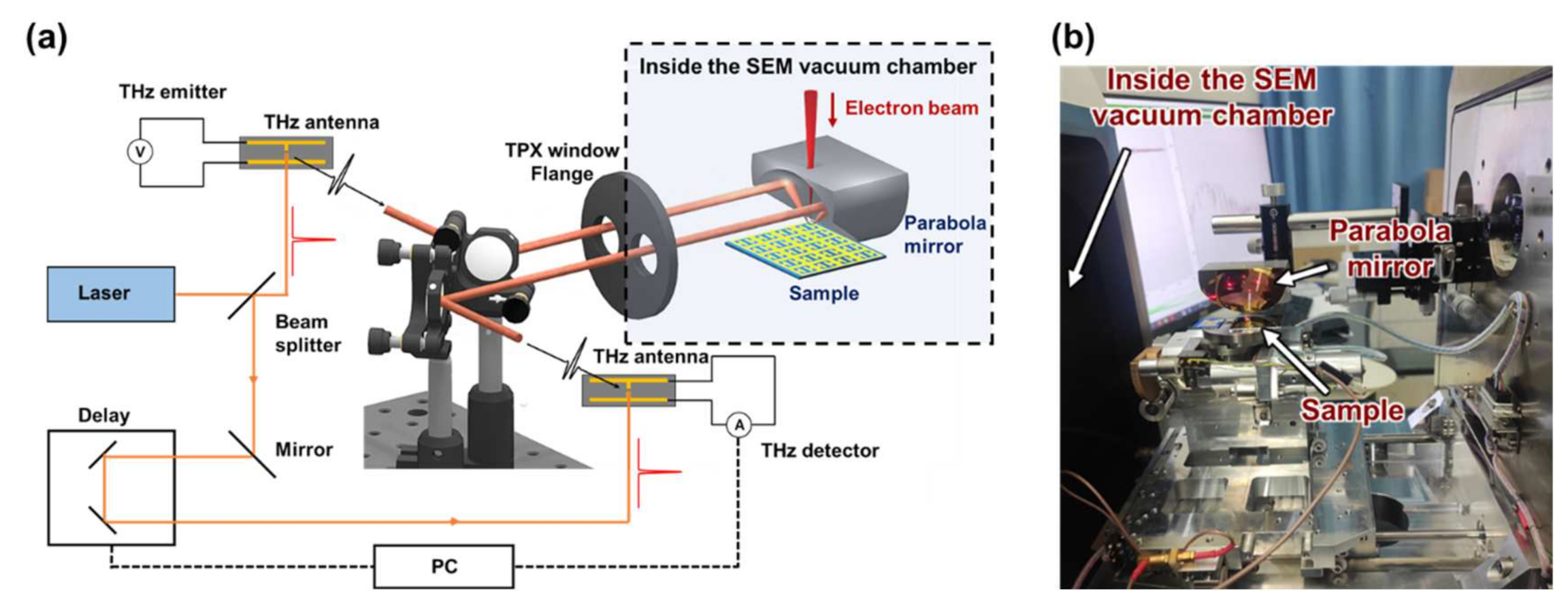
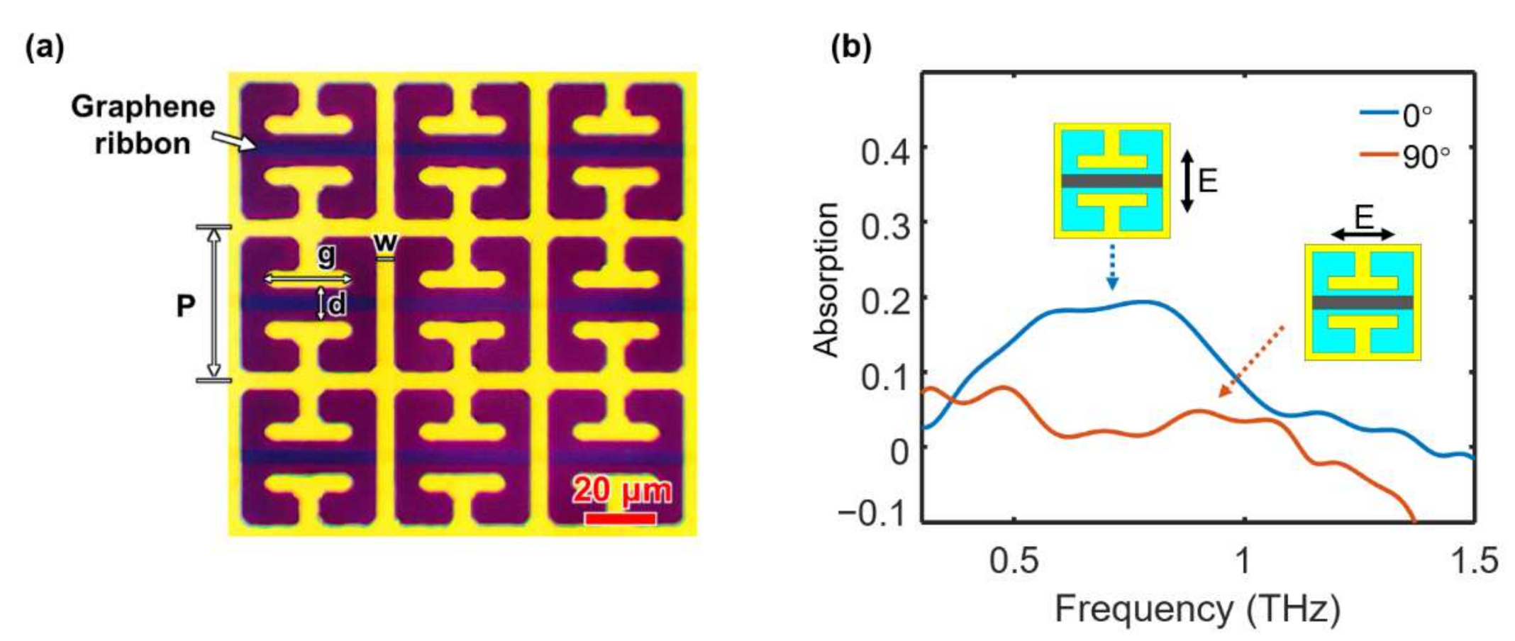
2. Materials and Methods

We combine the commercial SEM (Zeiss EVO-18) with THz-TDS (Menlo TeraSmart) to construct the self-developed SEM-TDS system. Specifically, TeraSmart is a terahertz time-domain spectrometer based on a photoconductive antenna and laser repetition frequency of 100 MHz and the frequency is from 0.2 to 2 THz. The upper right of Figure 1a shows the optical path inside the SEM cavity, and the rest is in the atmospheric conditions. The vacuum flange for the terahertz waves is made using a polymethylpentene (TPX) window, which has high transmittance in the terahertz band. The reflected terahertz optical path inside the cavity is realized by a 1 inch off-axis parabolic mirror. Figure 1b illustrates the SEM cavity door when it is open, corresponding to the interior of the cavity in Figure 1a. The angle of incidence with the vertical sample direction is about 26.5°. The spot diameter of terahertz is about 2~3 mm. The metamaterial sample is excited by free electrons passing through the small aperture of an off-axis parabolic mirror. It is possible to control the electron beam in a tiny area for precise modulation by SEM. Notably, free electrons can emit X-rays, and the TPX window is highly transparent to X-rays. Based on that, we design a radiation protection to cover all free space optical paths outside the cavity. Additionally, the radiation protection box is filled with nitrogen to reduce the effect of water vapor. The system manages to be the first ultra-accurate SEM-TDS system that combines electronics and photonics and contributes to further electron-matter interactions.
We designed a graphene-metal metamaterial. The proposed structure was fabricated on a 500 μm doped Si substrate (resistivity 1~10 Ω·cm) with a 300 nm dioxide layer. The gold metamaterial was patterned by photolithography, and then a 100 nm gold layer was sputtered on the substrate. The gold metamaterial was obtained by the next lift-off process. At last, CVD-grown graphene was transferred onto the substrate, and the graphene ribbons were fabricated by using a combination of photolithography and reactive ion etching processes. The gold metamaterial has a period P of 45 μm, a line width w of 5 μm, and g and d of 25 μm and 10 μm, respectively. The width of the graphene ribbon is 4 μm. We measured the frequency characteristic of absorption by A = 1 − (R/Rref)2. R is the amplitude of reflected signal of sample. Rref is the amplitude of the reflected signal of pure gold with SiO2/Si substrate as a reference. The absorption of the electric field perpendicular and parallel to the graphene ribbons are given in Figure 2b, with a 20% absorption at ~0.75 THz and zero absorption separately. This indicates that the graphene metamaterial resonates at ~0.75 THz when the electric field is perpendicular to the graphene ribbons. The resonant frequency measured in this experiment is consistent with the simulation.

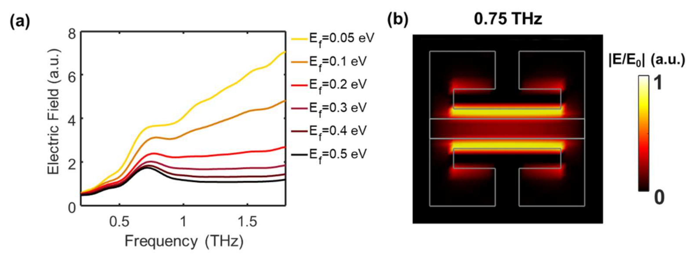
3. Results and Discussion

Keeping the electron beam voltage at 20 keV and the electron beam current from 0 μA to 2 μA, Figure 3 shows the time domain signals, frequency spectrum, and normalized spectrum with pure gold films on a silicon substrate as the reflection reference. The free electron beam has a beam spot size of 50 μm × 50 μm. It is shown that the free SEM-TDS system can achieve the precise tuning of metamaterials with minimal dimensions, which has critical applications for the accurate tuning of terahertz devices. The repeatability of this modulation is well, and the electron excitation region does not cause damage to the properties of the sample. As shown in Figure 3a, the modulation amplitude of the free electron excitation sample decreases in both time and frequency domain signals as the free electron beam current increases. The structure of the graphene-metal metamaterial in the reflection system has only the signal measured by reflection from the sample surface in the time domain signal. Figure 3 shows the resonance response absorption. The resonance amplitude of ~0.75 THz is reinforced with the increment of the electron beam current, accompanied by the weakening of the high frequency reflection. In our experiments, we start each measurement after changing the electron beam voltage or current for 30 s to ensure stable electron beam. Then, a 50-second integration of the terahertz signal is performed to improve the signal-to-noise ratio of the SEM-TDS. In those 50-second integrations, the terahertz signal is already stabilized and no longer varied with time. Therefore, the response time of the graphene device is smaller than 30 s. In the following, we analyze the modulation effect of graphene by simulations.
The experimental simulations are verified with CST Microwave Studio. A time-domain solver effectively tackles the periodicity with a 3 × 3 array structure. The boundary conditions in the X and Y directions are perfect electric and magnetic boundaries, respectively, with the electric field direction perpendicular to the direction of the graphene ribbons. There is an oxide layer with a dielectric constant of 4 between the substrate and the metal. The silicon substrate has a dielectric constant of 11.56 and a conductivity of 50 S/m. Located in the middle of the sample, the observation probe is 500 nm from the surface, which allows the direct observation of the near-field signals of the sample resonance, corresponding to the resonance response in the experiment. Figure 4a shows the terahertz response of the simulated graphene metamaterials with different graphene chemical potential obtained from the simulation. The simulated graphene relaxation time is 50 femtosecond. The temperature for both simulations and experiments is 293 K. The simulation results show that the resonant response of the graphene metamaterial increases with the decrease of the graphene chemical potential, and the amplitude increases. The trend of the spectra is consistent with the experimental measurements. Graphene is initially hole doped (p-type doping) due to chemical vapor deposition growth, transfer process, environmental impurities, and ribbons fabrication. As the experimental beam current climbs, the electrons are positively modulated on the graphene surface. The holes concentration, conductivity, as well as chemical potential of graphene gradually decrease. The graphene ribbons in the experiments are connected with metallic metamaterials between them, which can provide large-area of modulation. Compared to the simulated results, the experimental modulation of graphene is predicted to modulate from 0.5 eV to about 0.1 eV. From the field distribution of the graphene metamaterial with chemical potential 0.2 eV (see Figure 4b), it can be obtained that the electric field is mainly concentrated near the middle gap. As the chemical potential of graphene increases, the electrical conductivity also increases, thus weakening the strength of the local electric field and thus the resonant response of the metamaterial.
In order to exclude the effect of substrate doping on experiments, Figure 5 displays experimental measurements on silicon substrates at different electron beam currents. The reflection spectrum (see Figure 5b) manifest that the electron beam cannot be doped into the Si/SiO2 substrate due to the excellent isolation of the free electron beam by the 300 nm SiO2. The electron modulation results on the substrate further verify that the electron beam has a good modulation effect on the graphene metamaterials.

4. Conclusions

This paper demonstrates the electrical regulation of no-electrode graphene metamaterials by free electron beam in the experiment. A new SEM-TDS system is developed to observe the resonant response of metamaterials. Meanwhile, the resonance spectrum of graphene metamaterials with different graphene chemical potentials are investigated by simulations, which are in high consistency with the experimental results. The controllable SEM electron beam size can be adjusted to be tiny and the accurate local tuning experiments of no-electrode metamaterials perform well in this system. For example, an array of gating tunable devices consisting of individual components can be realized, and each component can be controlled independently by the precise local positioning of the SEM-TDS. In addition, this no-electrode metamaterial can significantly simplify the processing process and apply to various tunable two-dimensional natural materials. Even further, it can also be used for the electrical modulation of materials that are difficult to fabricate gate electrodes, such as topological insulators. It may reveal the complex electron–matter interaction between free electrons and other materials as well. To sum up, this creative approach paves the way for combining free-electron with photonics research, and realizing on-chip integrated, precisely tunable terahertz modulated devices.

Author Contributions

All authors made critical contributions to this work. All authors have read and agreed to the published version of the manuscript.

Funding

This research was funded by [National Key Research and Development Program of China] grant number [2017YFA0701000, 2020YFA0714001]; [Natural Science Foundation of China] grant number [61988102, 61921002, 62071108, 92163204]; [Fundamental Research Funds for the Central Universities] grant number [ZYGX2020ZB007].

Conflicts of Interest

The authors declare no competing interest.

References

  1. Ng, B.; Hanham, S.M.; Wu, J.; Fernández-Domínguez, A.I.; Klein, N.; Liew, Y.F.; Breese, M.B.H.; Hong, M.; Maier, S.A. Broadband terahertz sensing on spoof plasmon surfaces. ACS Photonics 2014, 1, 1059. [Google Scholar] [CrossRef]
  2. Brucherseifer, M.; Nagel, M.; Bolivar, P.H.; Kurz, H.; Bosserhoff, A.; Büttner, R. Label-free probing of the binding state of DNA by time-domain terahertz sensing. Appl. Phys. Lett. 2000, 77, 4049. [Google Scholar] [CrossRef] [Green Version]
  3. Zhang, S.; Wong, C.L.; Zeng, S.; Bi, R.; Tai, K.; Dholakia, K.; Olivo, M. Metasurfaces for biomedical applications: Imaging and sensing from a nanophotonics perspective. Nanophotonics 2021, 10, 259. [Google Scholar] [CrossRef]
  4. Hu, B.B.; Nuss, M.C. Imaging with terahertz waves. Opt. Lett. 1995, 20, 1716. [Google Scholar] [CrossRef] [PubMed]
  5. Yang, Z.; Tang, D.; Hu, J.; Tang, M.; Zhang, M.; Cui, H.L.; Wang, L.; Chang, C.; Fan, C.; Li, J.; et al. Near-Field Nanoscopic Terahertz Imaging of Single Proteins. Small 2021, 17, 2005814. [Google Scholar] [CrossRef]
  6. Qin, J.; Ying, Y.; Xie, L. The detection of agricultural products and food using terahertz spectroscopy: A review. Appl. Spectrosc. Rev. 2013, 48, 439. [Google Scholar] [CrossRef]
  7. Yang, X.; Zhao, X.; Yang, K.; Liu, Y.; Liu, Y.; Fu, W.; Luo, Y. Biomedical Applications of Terahertz Spectroscopy and Imaging. Trends Biotechnol. 2016, 34, 810. [Google Scholar] [CrossRef]
  8. Kim, T.T.; Kim, H.D.; Zhao, R.; Oh, S.S.; Ha, T.; Chung, D.S.; Lee, Y.H.; Min, B.; Zhang, S. Electrically tunable slow light using graphene metamaterials. ACS Photonics 2018, 5, 1800. [Google Scholar] [CrossRef] [Green Version]
  9. Jiang, L.; Yuan, C.; Li, Z.; Su, J.; Yi, Z.; Yao, W.; Wu, P.; Liu, Z.; Cheng, S.; Pan, M. Multi-band and high-sensitivity perfect absorber based on monolayer graphene metamaterial. Diam. Relat. Mater. 2021, 111, 108227. [Google Scholar] [CrossRef]
  10. Bianchi, V.; Carey, T.; Viti, L.; Li, L.; Linfield, E.H.; Davies, A.G.; Tredicucci, A.; Yoon, D.; Karagiannidis, P.G.; Lombardi, L.; et al. Terahertz saturable absorbers from liquid phase exfoliation of graphite. Nat. Commun. 2017, 8, 1. [Google Scholar] [CrossRef]
  11. Tao, H.; Landy, N.I.; Bingham, C.M.; Zhang, X.; Averitt, R.D.; Padilla, W.J. A metamaterial absorber for the terahertz regime: Design, fabrication and characterization. Opt. Express 2008, 16, 7181. [Google Scholar] [CrossRef] [PubMed]
  12. Lee, S.H.; Choi, M.; Kim, T.T.; Lee, S.; Liu, M.; Yin, X.; Choi, H.K.; Lee, S.S.; Choi, C.G.; Choi, S.Y.; et al. Switching terahertz waves with gate-controlled active graphene metamaterials. Nat. Mater. 2012, 11, 936. [Google Scholar] [CrossRef] [PubMed] [Green Version]
  13. Gopalan, P.; Sensale-Rodriguez, B.; Gopalan, P.; Sensale-Rodriguez, B. 2D Materials for Terahertz Modulation. Adv. Opt. Mater. 2020, 8, 1900550. [Google Scholar] [CrossRef]
  14. Yu, S.; Wu, X.; Wang, Y.; Guo, X.; Tong, L. 2D Materials for Optical Modulation: Challenges and Opportunities. Adv. Mater. 2017, 29, 1606128. [Google Scholar] [CrossRef] [PubMed]
  15. Pop, E.; Varshney, V.; Roy, A.K. Thermal properties of graphene: Fundamentals and applications. MRS Bull. 2012, 37, 1273. [Google Scholar] [CrossRef] [Green Version]
  16. Yu, L.; Dai, D.; He, S. Graphene-based transparent flexible heat conductor for thermally tuning nanophotonic integrated devices. Appl. Phys. Lett. 2014, 105, 251104. [Google Scholar] [CrossRef]
  17. Wen, Q.Y.; Tian, W.; Mao, Q.; Chen, Z.; Liu, W.W.; Yang, Q.H.; Sanderson, M.; Zhang, H.W. Graphene based All-Optical Spatial Terahertz Modulator. Sci. Rep. 2014, 4, 1. [Google Scholar] [CrossRef]
  18. Kim, T.T.; Oh, S.S.; Kim, H.D.; Park, H.S.; Hess, O.; Min, B.; Zhang, S. Giant Rashba splitting in 2D organic-inorganic halide perovskites measured by transient spectroscopies. Sci. Adv. 2017, 3, 1. [Google Scholar]
  19. Bonaccorso, F.; Sun, Z.; Hasan, T.; Ferrari, A.C. Graphene photonics and optoelectronics. Nat. Photonics 2010, 4, 611. [Google Scholar] [CrossRef] [Green Version]
  20. Deng, Y.; Zhou, Q.; Zhang, P.; Jiang, N.; Ning, T.; Liang, W.; Zhang, C. Heterointerface-Enhanced Ultrafast Optical Switching via Manipulating Metamaterial-Induced Transparency in a Hybrid Terahertz Graphene Metamaterial. ACS Appl. Mater. Interfaces 2021, 13, 13565. [Google Scholar] [CrossRef]
  21. Guo, B.; Fang, L.; Zhang, B.; Gong, J.R. Graphene Doping: A Review. Insci. J. 2011, 1, 80. [Google Scholar] [CrossRef] [Green Version]
Figure 1. (a) Schematic diagram of SEM-TDS system combined scanning electron microscopy and terahertz time-domain spectroscopy. The upper right is the light path inside the electron microscope cavity; (b) photograph of the light path inside the electron microscope cavity.
Photonics 09 00087 g001
Figure 2. (a) Optical micrograph of graphene metamaterial with the gold in yellow and the graphene ribbon in dark. (b) Absorption of the metamaterial when the electric field is perpendicular to the graphene ribbon and the electric field is parallel to the graphene ribbon.
Photonics 09 00087 g002
Figure 3. (a) Reflected time domain signal, (b) THz spectrum and (c) Absorption of graphene metamaterials from 0 to 2 μA at 20 keV electron beam.
Photonics 09 00087 g003
Figure 4. (a) simulated spectrum of graphene metamaterials with graphene chemical potential from 0.05 eV to 0.5 eV. (b) Electric field distribution of graphene metamaterial at 0.75 terahertz.
Photonics 09 00087 g004
Figure 5. (a) Time domain signal of 0~2 μA for SiO2/Si substrate at 20 keV. (b) Normalized spectra of 1 μA and 2 μA to 0 μA.
Photonics 09 00087 g005
Publisher’s Note: MDPI stays neutral with regard to jurisdictional claims in published maps and institutional affiliations.

