1. Introduction
At present, mid-infrared (3 < λ < 5 μm) semiconductor lasers are primarily sold as individually packaged units. InP-based quantum cascade lasers (QCLs) are a prime example, with access to the entire spectral range and demonstrating records for both output power (200 W) and efficiency (31%) within this band [
1,
2]. Nevertheless, costs for individual QCLs are still quite high, partly due to the limited number of laser manufacturers and limited number of lasers that can be obtained per wafer. InP substrates typically have a diameter of 100 mm or less, compared to Si, which can reach diameters of 450 mm. State-of-the-art fabrication equipment is also available for larger wafers, which can also improve yield and reduce costs. Therefore, direct production of QCLs on Si has the potential to drastically change the cost per laser and make the technology much more accessible to the general scientific community. The other benefit of this approach is the potential to create custom mi-infrared photonic circuits through massive integration of mid-infrared active optoelectronic components on a low cost photonic platform.
If technically feasible, the most straightforward integration method is the direct epitaxial growth of QCLs on Si wafers. The primary challenge in this case is maintaining the crystalline quality and sharp interfaces of the QCL in the presence of lattice constant and/ or thermal expansion mismatch. Si has an 8% lattice constant mismatch and ~50% thermal expansion coefficient mismatch with respect to InP, which is been a significant technical hurdle to overcome. A similar challenge has been tackled in the past for InP-based 1.3–1.55 μm lasers on Si, though, which gives hope that this is possible for QCLs as well [
3,
4]. In this earlier work, a dislocation density as low as 1.5 × 10
8 cm
−2 was achieved for an InP-on-Si template.
Other groups have attempted this strategy already. Long wavelength (λ > 8 μm) InAs-based QCLs were demonstrated at room temperature [
5]. InP-based QCLs, which would ideally have better performance, have not been as successful, with either only electroluminescence observed [
6] or operation up to 170 K at a wavelength of 4.3 μm [
7]. Recently, our group made a breakthrough intermediate demonstration of a high power mid-infrared InP-based QCL on GaAs [
8], which has approximately half the lattice mismatch (4%) compared to Si. This process continues in this paper, with demonstration of the first strain-balanced, mid-infrared QCL with high power output at room temperature.
2. Materials and Methods
In order to grow an InP-based QCL on a Si wafer, a suitable template must be prepared that can transition from the lattice constant of Si to InP and provide a smooth starting surface. For this work, the template was grown entirely by gas-source molecular beam epitaxy (GSMBE).
The starting surface of the template is a (001) 2-inch Si wafer (p-type) that is 4° miscut toward the [110] direction. A 1 μm thick layer of GaAs is deposited at a growth temperature of 600 °C and a growth rate of 0.5 μm/h. Thermal cycle annealing (TCA) is used during this layer to help reduce the dislocation density on the surface [
9]. The TCA cycle for this template involves heating to 750 °C during 12 min, annealing for 5 min, and then cooling to 300 °C during 12 min. 6 TCA steps are utilized in total.
Following GaAs growth, a transition is made to InP, with a 100 nm film deposited at 400 °C at a rate of 0.5 μm/h. The wafer temperature is then raised to 570 °C where a 5 nm/ 5 nm Ga
0.467In
0.533As/ InP superlattice (SL) is used as a dislocation filter [
10]. For this template, 5 SL periods are deposited at a time, followed by a 100 nm InP layer. This sequence is repeated 5 times.
Part of the lower contact and waveguide cladding layers are then deposited. This starts with 1 μm of n+ InP (Nd = 1 × 1018 cm
−3) and 50 nm of n+ Ga
0.467In
0.533As (N
d = 1 × 10
18 cm
−3). Next, a 2 μm n- InP layer (N
d = 2 × 10
17 cm
−3) and a 1.5 μm n- InP layer (N
d = 2 × 10
16 cm
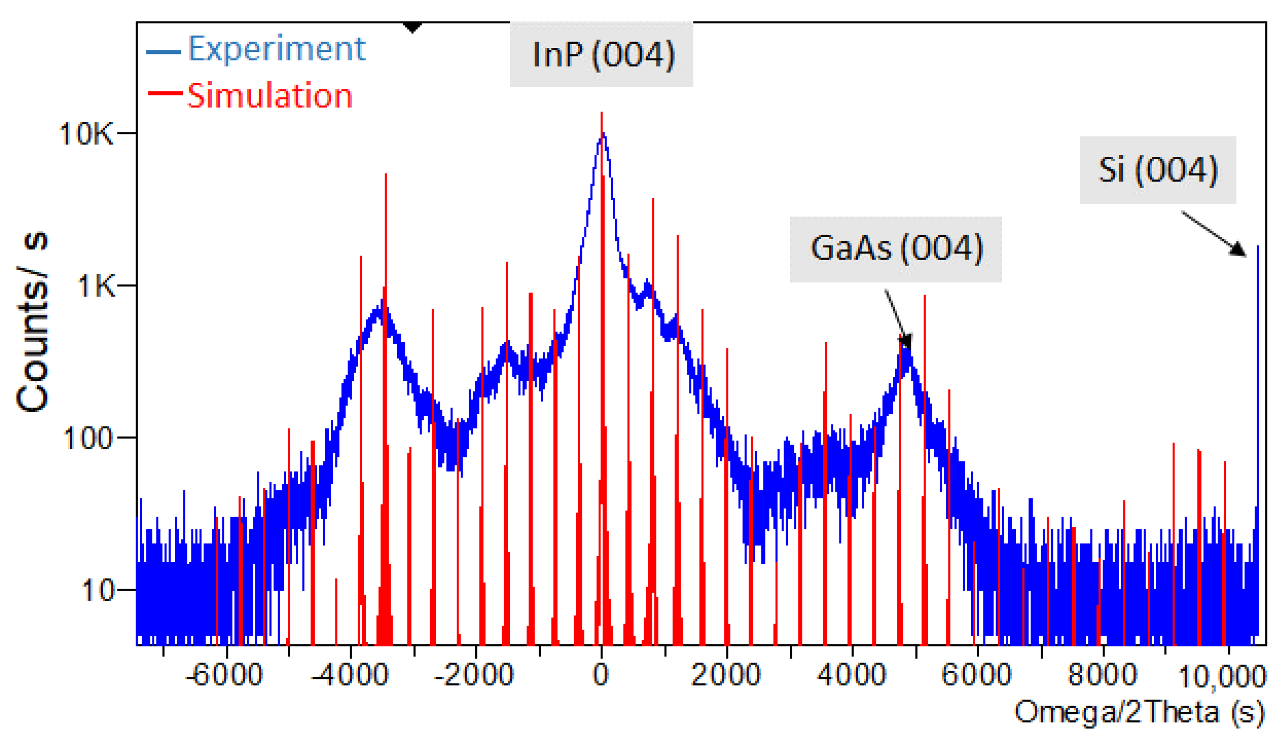
−3) are deposited to finish the template. The template is visually smooth, with a rms roughness of 1.88 nm measured by atomic force microscopy over a 100 μm
2 area. This is significantly better than the as-grown template demonstrated in Ref. [
6] (6.89 nm roughness), but somewhat rougher than the demonstration in Ref. [
7] (0.7 nm roughness).
The band structure of the QCL core is based on the shallow-well design in [
11], which utilizes a strain-balanced band structure for improved electron confinement. This is also the same core structure used by our group for the demonstration of a high power MWIR QCL on GaAs [
8]. Identical layer sequences and environmental conditions are used for growth of a 40-stage, mid-infrared high-efficiency laser core on the InP-coated Si template described above. Growth of the QCL core began with an additional 0.5 μm thick n- InP layer (N
d = 2 × 10
16 cm
−3) to complete the lower waveguide cladding. On top of the laser core, a 100 nm thick n-InP layer (N
d = 2 × 10
16 cm
−3) is grown, followed by 300 nm thick n-GaInAs (N
d = 2 × 10
16 cm
−3) and a 20 nm thick n-InP layer (N
d = 2 × 10
16 cm
−3). The wafer is then transferred to a low pressure metalorganic chemical vapor deposition (LP-MOCVD) reactor, where a 3 μm thick n-InP cladding layer (N
d ramped from 2–20 × 10
16 cm
−3) and a 1 μm thick n+ InP cap layer (N
d = 1 × 10
19 cm
−3) are grown.
The InP-on-Si template has integrated contact layers to facilitate the use of two contacts on the epitaxial (top) side of the wafer. This avoids extra resistance through the heterointerfaces [
8] and makes the process inherently compatible with the use of high resistivity Si or silicon-on-insulator (SOI) wafers in the future.
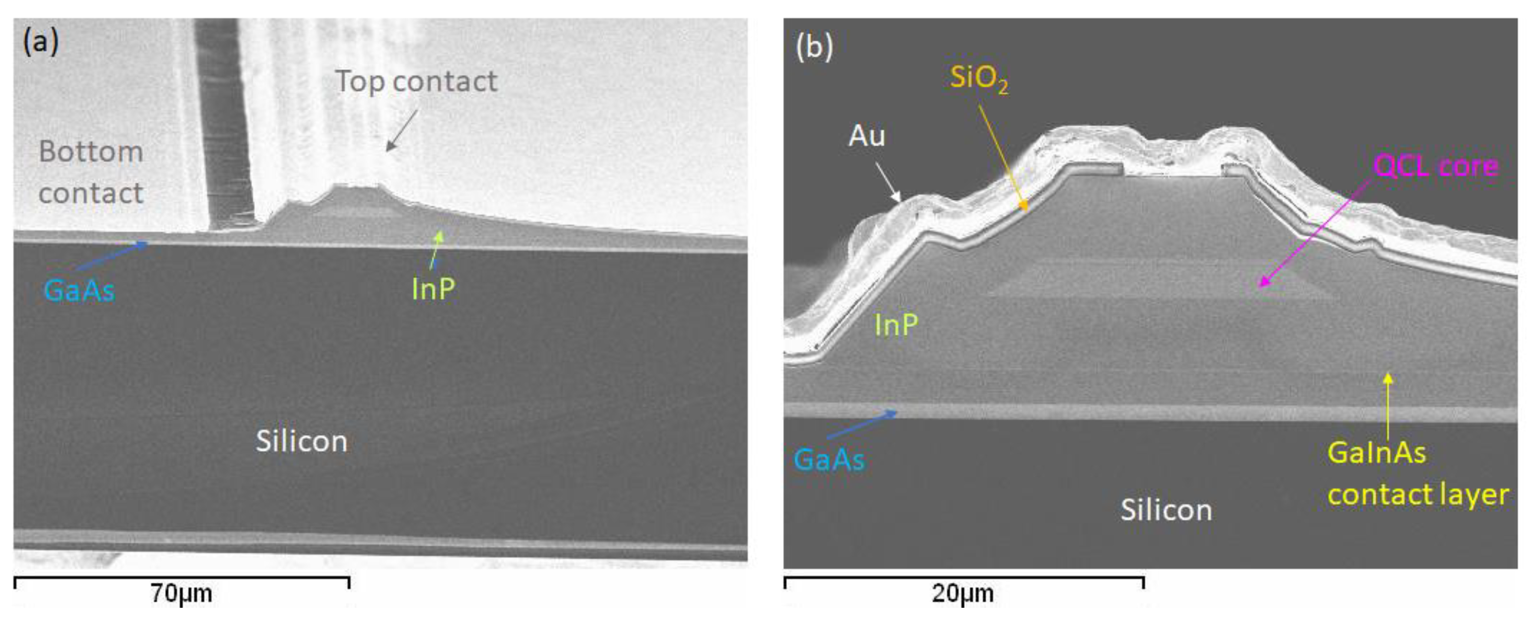
The complete wafer was processed into a buried heterostructure waveguide with a core width of ~17 μm. After chemically etching the waveguide core, semi-insulating Fe-doped InP was regrown around the core using LP-MOCVD. SiO
2 is used as an insulator everywhere except on the very top of the waveguide and in the bottom contact region, which is ~25 μm away from the laser core. Current travels vertically through the laser core from the top contact and laterally from the core to the bottom contact. The Fe-doped InP is used to reduce the lateral waveguide losses due to sidewall scattering at the SiO
2/ Au interface. The contact metal is Ti/Au which is then electroplated with a thick (~2 μm) Au layer. Prior to cleaving the wafer into discrete devices, the Si wafer was thinned to ~65 μm. Oblique and cross-sectional views of a cleaved laser facet, measured by a scanning electron microscope (SEM) are shown in
Figure 1. Clear demarcations between the Si substrate, GaAs buffer, and InP-based layers are observed, and the cleaved laser facet is extremely flat near the laser core.
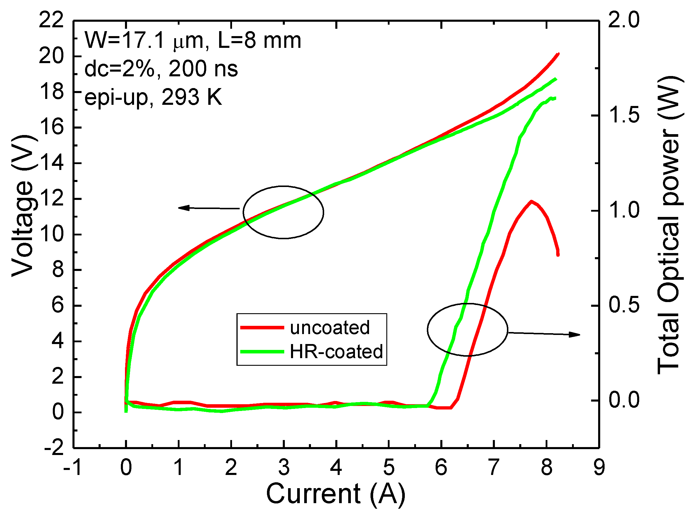
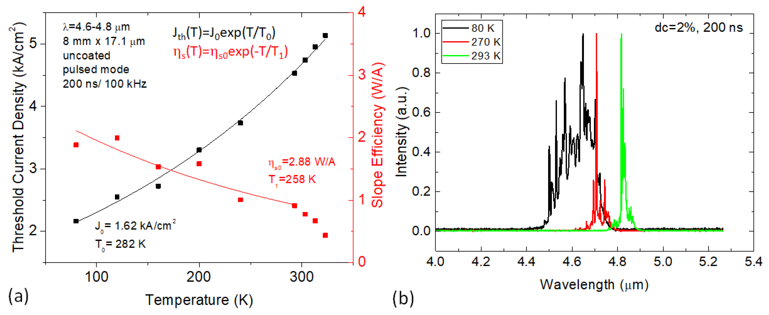
For testing, an 8 mm long laser bar was cleaved, and some of the lasers had the rear mirror facet high reflection (HR) coated with Y2O3/Ti/Au. Laser bars were mounted epilayer-up with indium to copper heat sinks. For cryogenic testing (80–293 K), the laser was placed in a liquid nitrogen cryostat) and power was collected through an anti-reflection coated ZnSe window. At temperatures of 293 K and above, the laser heat sink was mounted on a thermoelectric stage, and the temperature was monitored by a thermistor.
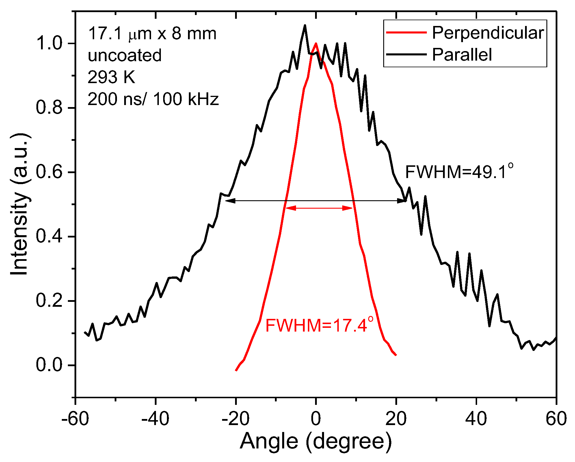
Laser testing was done in pulsed mode using 200 ns pulses at a repetition rate of 100 kHz. Average power is measured by a calibrated thermopile detector placed in close proximity to the front laser facet. Peak power is calculated by dividing average power by the pulsed duty cycle (0.02). For uncoated lasers, the total power from both mirror facets is calculated by multiplying the measured power by 2. Spectral measurements are also done in pulsed mode, using a high resolution (0.125 cm−1) Bruker IFS 66v/S FTIR and a deuterated triglycine sulfate (DTGS) detector. For measurements of the laser far field emission, the laser was centered on a rotating stage and measured with a HgCdTe detector with a 1.5 mm aperture at a distance of 30 cm.
4. Discussion
These results represent a significant improvement over past results [
6,
7] for mid-infrared QCLs on Si, with about a 180 K increase in operating temperature. However, the current density is generally too high to support continuous wave operation at this time. It is likely that the rougher surface observed on the completed wafer is an indication of a gradual breakdown in the superlattice structure during the laser core growth. This may or may not be influenced by the strain-balanced laser core, in which relaxation may be facilitated by a high dislocation density (>10
8 cm
−2) still present on the wafer surface. The breakdown in the superlattice structure would gradually lead to broadening of the intersubband gain curve and an increase in free carrier absorption within the laser core. In this case, the laser would exhibit a reduced differential gain and increased threshold current density, as seen above. Another consequence of this situation would be a possible decrease in carrier confinement, due a reduced barrier height, which could lead to the lower T
0 and T
1 values observed. Nevertheless, the fact that the laser worked so well in the presence of such a high dislocation density shows some evidence that an intersubband laser may be more tolerant of dislocations than a traditional interband diode laser.
It is clear that some improvement is needed to stabilize the laser core during growth. The first goal is to produce a smoother wafer surface, with fewer dislocations, on which to grow the laser core superlattice. A typical InP-based QCL core has an rms roughness of <0.2 nm. The QCL on GaAs developed in Ref. [
8], which also had very good performance, had an rms roughness of around 2 nm. These are both significantly lower than the 9.4 nm rms roughness exhibited by the current wafer. However, roughness is not the only variable, as the laser from Ref. [
7] had roughness of only 3.8 nm but failed to operate above 170 K. This problem needs to be studied further.
Through additional optimization of the InP-on-Si template, laser core growth conditions, and possible modification of the strain level in the laser core, it is expected that the rms roughness of the laser core can be reduced to below 1 nm with a dislocation density in the 107 cm−2 range. In this case, it is believed that laser performance can be improved significantly.


