Communication

Improved Tunneling Property of p+Si Nanomembrane/n+GaAs Heterostructures through Ultraviolet/Ozone Interface Treatment

1
School of Electronics and Information Engineering, Korea Aerospace University, Goyang 10540, Republic of Korea
2
School of Electronics Engineering, Kyungpook National University, Daegu 41566, Republic of Korea
*
Authors to whom correspondence should be addressed.
Inorganics 2022, 10(12), 228; https://doi.org/10.3390/inorganics10120228
Submission received: 27 September 2022 / Revised: 22 November 2022 / Accepted: 25 November 2022 / Published: 28 November 2022
(This article belongs to the Section Inorganic Materials)

Abstract

:
Here, heterostructures composed of p+Si nanomembranes (NM)/n+GaAs were fabricated by ultraviolet/ozone (UV/O3, UVO) treatment, and their tunneling properties were investigated. The hydrogen (H)-terminated Si NM was bonded to the oxygen (O)-terminated GaAs substrate, leading to Si/GaAs tunnel junctions (TJs). The atomic-scale features of the H-O-terminated Si/GaAs TJ were analyzed and compared to those of Si/GaAs heterojunctions with no UVO treatment. The electrical characteristics demonstrated the emergence of negative differential resistance, with an average peak-to-valley current ratio of 3.49, which was examined based on the band-to-band tunneling and thermionic emission theories.

Graphical Abstract

1. Introduction

In recent years, the demands for low-power electronic devices have increased due to the realization of artificial intelligence (AI) technology. A tunnel junction (TJ) diode is a representative source of low-power circuits with a negative differential resistance (NDR) phenomenon via the quantum mechanical tunneling of carriers passing through the energy bands [1,2,3,4,5]. To realize the TJ, the construction of energy bandgaps of highly doped, staggered (II), or broken (III) types is necessary. Several experiments have attempted to acquire crystalline Si/GaAs heterostructures for application in high-speed operation [6,7,8,9]. Since there exist crystal dislocations at the epitaxially grown Si/GaAs interface due to a lattice mismatch, junction bonding techniques were adopted to achieve the heterostructure. The nanomembrane (NM) transfer printing technique allows one to obtain a deterministic assembly of semiconductors with different lattice constants and doping concentrations, leading to the construction of heterojunctions with diverse material combinations and designed bandgap structures [6,10,11,12,13,14]. The main issue that impedes the conduction of heterojunctions is the generation of the interface layer during the bonding process, which deforms the energy bandgap and obstructs the carriers’ injection. The ultraviolet/ozone (UV/O3, UVO) treatment is a multipurpose process that is proven to be an effective surface passivation method for Ga-based compound semiconductors [15,16,17]. It was proved that the surface energy and interface state density were improved through the UVO treatment.
In this work, TJ diodes comprised of p+Si NM/n+GaAs were fabricated by UVO treatment, and the mechanism for the improved tunneling property was investigated. The hydrogen (H)-terminated Si NM was laminated on the oxygen (O)-terminated GaAs substrate for the formation of the H-O interface. The atomic features of the Si/GaAs interface developed by UVO treatment were inspected by scanning transmission electron microscopy (STEM). The electrical characteristics of the Si/GaAs TJs exhibited an NDR region with an improved tunneling property, which was explained according to the band-to-band tunneling (BTBT) and thermionic emission (TE) principles.

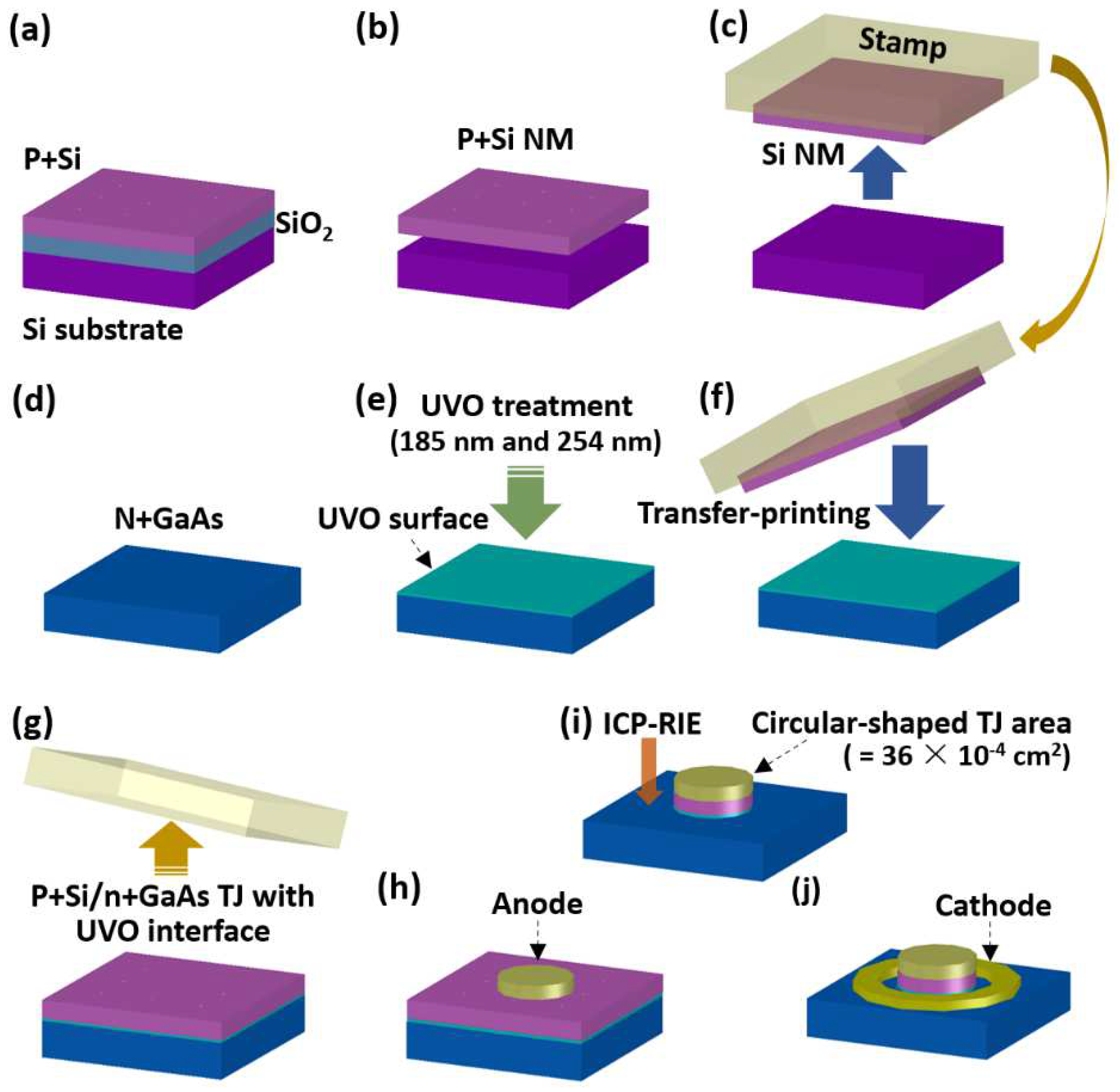
2. Results and Discussion

Figure 1a depicts the vertical crystalline properties of the Si/GaAs TJ interface subjected to UVO treatment. The Si and GaAs comprise of crystal structures of diamond cubic with a lattice constant of 5.43 Å and zinc blende with a lattice constant of 5.65 Å, respectively. Due to the high energy difference due to the lattice mismatch at the TJ interface, it is preferable to develop an interlayer that binds the junction interface, so that this causes the state of the interface energy to be stable [10]. Previous results for Si/GaAs heterojunctions with no UVO treatment demonstrated the growth of the amorphous interlayer, which causes the interface energy to be lower than that of the other structures, such as poly-crystals and single crystals [6]. However, the amorphous layer can work as an energy barrier that impedes the carriers’ flow across the TJ energy bands, obstructing the performance of the TJ. To enhance the tunneling property of the heterostructure, the growth of the interlayer should be minimized. Since the density of the coincident lattice sites at the Si/GaAs interface is low and the spacing of the screw dislocations is short, the position of the interfacial atoms was rearranged into a shape that could enable covalent bonding on the surfaces during the Si/GaAs bonding. The UVO treatment was employed to modify the surface morphology and termination of the GaAs, which affect the growth of the interlayer of the Si/GaAs heterostructure. It was reported that the surface roughness of the GaAs was improved with the UVO treatment due to the absorption of O atoms adjacent to the GaAs surface [18]. The improvement of the surface morphology can lower the density and location of the screw dislocations on the GaAs surface, which can increase the density of the coincident lattice sites at the Si/GaAs interface and lessen the necessity for the energetical generation of an amorphous interlayer.
Figure 1b exhibits the STEM image of the Si/GaAs interface subjected to UVO treatment. Though previous research demonstrated that an approximately 2 nm-thick amorphous layer was formed at the interface with no UVO treatment, here, few atomic layers were observed at the Si/GaAs interface, presumably owing to the increased density of the coincident lattice sites at the Si/GaAs interface due to the UVO treatment. The diffusion of the elements into the interlayer is likely to be negligible at the 375 °C bonding temperature. The twist angle between the atomic lattices of Si and GaAs was generated during the junction bonding, which affected the resolution of the atomic properties at the interface.
Based on the van der Waals (vdW) acoustic mismatch model (AMM), the ITR was associated with phonon transport through the interfaces [12,19,20]. Several results confirmed that the higher operating temperature decreased the tunneling properties of the tunnel diodes, including a decreased peak-to-valley current ratio (PVCR) value [21,22,23]. To improve the tunneling performance of the Si/GaAs TJ, a low ITR value at the junction interface is preferred. It was reported that the bonding energy at the vdW-bonded Si/Si H-O interface (60 mJ/m2) was higher than that of the H-H interface (30 mJ/m2), and the corresponding ITR at the H-O interface (2.8 m2K/GW) was lower than that of the H-H interface (9.2 m2K/GW) [12]. Since the Si/GaAs heterostructure consists of H-terminated Si and O-terminated GaAs, the Si/GaAs TJ features an H-O interface and lower ITR than that of the non-UVO-treated interface.
The electrical characteristics (J-V) of the Si/GaAs TJs were explored in the bias range from −2 V to 2 V at room temperature, in which the different conduction mechanisms for the charge carriers’ flow were observed according to the input bias (Figure 2a). The ohmic contact characteristics of the individual anode and cathode were confirmed prior to the analysis of the tunneling conduction at the TJ interface. Two regions appeared: BTBT under the bias of 1.07 V (A) and TE over the bias of 1.10 V (B). There existed an NDR area between the BTBT and TE regions, where the average PVCR was determined to be 3.49 (Figure 2b). The emergence of the NDR was ascribed to the charge carriers’ tunneling across the energy bands of the Si/GaAs heterostructure. The improvement of 50.4% in the PVCR value compared to the value of the Si/GaAs TJ with no UVO treatment (2.32) in the previous study was confirmed, which can possibly be attributed to the suppressed interlayer growth and the decreased ITR at the Si/GaAs interface due to the UVO treatment. Compared to the PCVR values reported by other groups, with values of 1.30 for Si TJ and 1.45 for GaN/AlN TJ, the PVCR in this work verifies the improvement of the tunneling property through the interface treatment [24,25].
For the further analysis of the charge carriers’ behavior in the individual conduction regions of the p+Si/n+GaAs abrupt TJs, the J-V curve was divided into A and B regions, and fitting was performed using software on the assumption that the same conduction principle was maintained throughout the whole bias range. The BTBT curve in Figure 2c with the red dashed line, plotted by the fitting out of the bias range from the BTBT region, shows the odd function behavior due to the interchangeable direction of the carriers’ injection across the energy bands. The TE curve in Figure 2d displayed with the red dashed line, plotted by fitting, represents the exponential function behavior due to the carriers’ flow along the energy bands. The insets in Figure 2c,d represent the direction of the carriers’ injection across the energy band in the diagrams.

3. Materials and Methods

Si features a high hole mobility (≤450 cm2/V∙s) and quantum phenomenon associated with its thickness, in addition to the low-cost production capability and complementary metal-oxide-semiconductor process compatibility. A GaAs that is a compound semiconductor has a high electron mobility (≤8500 cm2/V∙s) and high-speed applications, such as monolithic microwave integrated circuits and heterostructure-based transistors. Through the formation of p+Si and n+GaAs heterojunctions with high doping concentrations and carrier mobilities, the production of TJs with abrupt energy bands and bipolar junctions, together with high-speed operations, is feasible. The processing steps for p+Si/n+GaAs TJs created by UVO treatment start with the preparation of a Si-on-insulator wafer (SOI, Si/SiO2 = 100/1000 nm) with a boron doping concentration of 1 × 1019 cm–3 (Figure 3a). Here, the undercutting of the sacrificial oxide layer was carried out by dipping NM-patterned SOI into a 49% hydrofluoric acid (HF) solution for 10 min (Figure 3b). The single-crystalline Si NM on the Si substrate was gathered using an elastomeric stamp prior to transfer printing (Figure 3c). The H-terminated surface appeared on the bottom side of Si NM after the HF undercut. The GaAs substrate was grown by metal-organic chemical vapor deposition with a Si doping concentration of 1 × 1019 cm−3 (Figure 3d). The GaAs was loaded into a process chamber to undergo UVO treatment under active wavelengths of 185 nm and 254 nm of the hot cathode and a low-pressure mercury lamp, respectively, with an O2 dose rate of 7 mg/L for 6 min. The 185 nm UV light dissociates molecular O2 into triplet atomic O (3P) that forms O3 by combination with the molecular O2. The 254 nm UV light then dissociates the O3 into molecular O2 and single atomic O (1D) that reacts with the GaAs surface (Figure 3e). The O-terminated surface was formed on the top side of the GaAs after the UVO treatment. The deterministic transfer printing was performed by laminating the hydrogen-terminated Si NM on the target spot of the oxygen-terminated GaAs (Figure 3f), leading to the formation of crystalline UVO-treated p+Si/n+GaAs heterostructures (Figure 3g). The hydrophilicity induced by the UVO treatment changes the surface energy and junction bonding strength [17]. The Si/GaAs TJs were bonded in the rapid thermal annealing chamber at 375 °C for 5 min. To define the tunneling region, the circular-shaped TJ area of 36 × 10−4 cm2 was patterned on the Si/GaAs heterojunctions using a mask aligner for photolithography, followed by the deposition of Ni/Au on the anode electrode (Figure 3h). The mesa-structure of the cathode was formed by inductively coupled plasma-reactive ion etching (Figure 3i), followed by the patterning of the ground electrode and deposition of the Pd/Ge/Au, with subsequent ohmic annealing at 375 °C for 5 min (Figure 3j).

4. Conclusions

The improved tunneling property of the p+Si NM/n+GaAs heterostructures with UVO-treated interfaces was investigated, and the principles of the conduction were analyzed based on the BTBT and TE. The suppressed growth of the interlayer can possibly be ascribed to the increased density of the coincident lattice sites at the Si/GaAs interface due to the change in the GaAs surface morphology due to the UVO treatment. The atomic-scale properties of the Si/GaAs interface were analyzed using STEM. The Si/GaAs junction interface of the H-O termination may lead to a decreased ITR with respect to that of the non-UVO-treated interface. Compared to the previous research on Si/GaAs TJs with no interface treatment, this work demonstrated the effects of UVO interface treatment on the tunneling property of the Si/GaAs heterostructure through the analysis of the restrained growth of the interlayer and conduction principles. The mechanism of the improved tunneling property was explained by the changes in the density of the dislocations and thermal capability at the interface. The results of the improved tunneling performance through the UVO treatment are applicable to the construction of electronic devices with interfaces comprised of different crystal structures.

Author Contributions

Conceptualization, K.K. and J.J.; investigation, K.K. and J.J.; writing, K.K. and J.J.; project administration, K.K. All authors have read and agreed to the published version of the manuscript.

Funding

This research was funded by the National Research Foundation of Korea (NRF) Grant, funded by the Korean Government (MSIT) under grant 2020R1F1A1066175. This research was funded by 2021 Korea Aerospace University Faculty Research Grant.

Institutional Review Board Statement

Not applicable.

Informed Consent Statement

Not applicable.

Conflicts of Interest

The authors declare no conflict of interest.

References

  1. Wang, X.; Wang, J. Ferroelectric tunnel junctions with high tunnelling electroresistance. Nat. Electron. 2020, 3, 440. [Google Scholar] [CrossRef]
  2. Hase, Y.; Komori, Y.; Kusumoto, T.; Harada, T.; Seki, J.; Shiga, T.; Kamiya, K.; Nakanishi, S. Negative differential resistance as a critical indicator for the discharge capacity of lithium-oxygen batteries. Nat. Commun. 2019, 10, 596. [Google Scholar] [CrossRef] [Green Version]
  3. Shim, J.; Oh, S.; Kang, D.-H.; Jo, S.-H.; Ali, M.H.; Choi, W.-Y.; Heo, K.; Jeon, J.; Lee, S.; Kim, M.; et al. Phosphorene/rhenium disulfide heterojunction-based negative differential resistance device for multi-valued logic. Nat. Commun. 2016, 7, 13413. [Google Scholar] [CrossRef] [PubMed] [Green Version]
  4. Yan, R.; Fathipour, S.; Han, Y.; Song, B.; Xiao, S.; Li, M.; Ma, N.; Protasenko, V.; Muller, D.A.; Jena, D.; et al. Esaki diodes in van der Waals heterojunctions with broken-gap energy band alignment. Nano Lett. 2015, 15, 5791. [Google Scholar] [CrossRef] [Green Version]
  5. Liu, X.; Qu, D.; Li, H.-M.; Moon, I.; Ahmed, F.; Kim, C.; Lee, M.; Choi, Y.; Cho, J.H.; Hone, J.C.; et al. Modulation of quantum tunneling via a vertical two-dimensional black phosphorus and molybdenum disulfide p-n junction. ACS Nano 2017, 11, 9143. [Google Scholar] [CrossRef]
  6. Kim, K.; Jang, J.; Kim, H. Negative differential resistance in Si/GaAs tunnel junction formed by single crystalline nanomembrane transfer method. Results Phys. 2021, 25, 104279. [Google Scholar] [CrossRef]
  7. Liang, J.; Miyazaki, T.; Morimoto, M.; Nishida, S.; Watanabe, N.; Shigekawa, N. Electrical properties of Si/Si interfaces by using surface-activated bonding. Appl. Phys. Express 2013, 6, 021801. [Google Scholar] [CrossRef]
  8. Zhao, Y.; Bao, W.L.; Yang, F.; Wang, X. Plasma-activated GaAs/Si wafer bonding with high mechanical strength and electrical conductivity. Mater. Sci. Semicond. 2022, 143, 106481. [Google Scholar] [CrossRef]
  9. Zhou, Y.C.; Zhu, Z.H.; Crouse, D.; Lo, Y.H. Electrical properties of wafer-bonded GaAs/Si heterojunctions. Appl. Phys. Lett. 1998, 73, 2337. [Google Scholar] [CrossRef]
  10. Kiefer, A.M.; Paskiewicz, D.M.; Clausen, A.M.; Buchwald, W.R.; Soref, R.A.; Lagally, M.G. Si/Ge Junctions Formed by Nanomembrane Bonding. ACS Nano 2011, 5, 1179. [Google Scholar] [CrossRef] [PubMed]
  11. Liu, T.C.; Kabuyanagi, S.; Nishimura, T.; Yajima, T.; Toriumi, A. n+Si/pGe heterojunctions fabricated by low temperature ribbon bonding with passivating interlayer. IEEE Electron. Device Lett. 2017, 38, 716. [Google Scholar] [CrossRef]
  12. Schroeder, D.P.; Aksamija, Z.; Rath, A.; Voyles, P.M.; Lagally, M.G.; Eriksson, M.A. Thermal resistance of transferred-silicon-nanomembrane interfaces. Phys. Rev. Lett. 2015, 115, 256101. [Google Scholar] [CrossRef] [Green Version]
  13. Hwang, S.-W.; Lee, C.H.; Cheng, H.; Jeong, J.-W.; Kang, S.-K.; Kim, J.-H.; Shin, J.; Yang, J.; Liu, Z.; Ameer, G.A.; et al. Biodegradable elastomers and silicon nanomembranes/nanoribbons for stretchable, transient electronics, and biosensors. Nano Lett. 2015, 15, 2801. [Google Scholar] [CrossRef]
  14. Tai, Y.-C.; Yeh, P.-L.; An, S.; Cheng, H.-H.; Kim, M.; Chang, G.-E. Strain-free GeSn nanomembranes enabled by transfer-printing techniques for advanced optoelectronic applications. Nanotechnology 2020, 31, 445301. [Google Scholar] [CrossRef]
  15. Kim, K.; Kim, T.J.; Zhang, H.; Liu, D.; Jung, Y.H.; Gong, J.; Ma, Z. AlGaN/GaN Schottky-Gate HEMTs with UV/O3-Treated Gate Interface. IEEE Electron. Device Lett. 2020, 41, 1488. [Google Scholar] [CrossRef]
  16. Kim, K.; Liu, D.; Gong, J.; Ma, Z. Reduction of leakage current in GaN Schottky diodes through ultraviolet/ozone plasma treatment. IEEE Electron. Device Lett. 2019, 40, 1796. [Google Scholar] [CrossRef]
  17. Kim, K.; Kim, J.; Gong, J.; Liu, D.; Ma, Z. Metal-Al2O3-GaN capacitors with an ultraviolet/ozone plasma-treated interface. Jpn. J. Appl. Phys. 2020, 59, 030908. [Google Scholar] [CrossRef]
  18. Gao, J.; Xiao, C.; Feng, C.; Wu, L.; Yu, B.; Qian, L.; Kim, S.H. Oxidation-induced changes of mechanochemical reactions at GaAs-SiO2 interface: The competitive roles of water adsorption, mechanical property, and oxidized structure. Appl. Surf. Sci. 2021, 548, 149205. [Google Scholar] [CrossRef]
  19. Aksamija, Z.; Knezevic, I. Thermal conductivity of Si1-xGex/Si1-yGey superlattices: Competition between interfacial and internal scattering. Phys. Rev. B 2013, 88, 155318. [Google Scholar] [CrossRef] [Green Version]
  20. Prasher, R. Acoustic mismatch model for thermal contact resistance of van der Waals contacts. Appl. Phys. Lett. 2009, 94, 041905. [Google Scholar] [CrossRef]
  21. El-Basit, W.A.; Awad, Z.I.M.; Kamh, S.A.; Soliman, F.A.S. Temperature dependence of backward tunnel diode oscillator circuit. Microelectron. J. 2020, 99, 104756. [Google Scholar] [CrossRef]
  22. Wilson, A.A.; Jankowski, N.R.; Nouketcha, F.; Tompkins, R. Kapitza Resistance at the Two-Dimensional Electron Gas Interface. In Proceedings of the Intersociety Conference on Thermal and Thermomechanical Phenomena in Electronic Systems, Las Vegas, NV, USA, 28–30 May 2019. [Google Scholar]
  23. Lee, J.; Choi, S.; Yang, K. Temperature dependence characteristics of InP RTD based CML-mobile D-flip flop IC. In Proceedings of the 2009 IEEE International Conference on Indium Phosphide & Related Materials, Newport Beach, CA, USA, 10–14 May 2009. [Google Scholar]
  24. Dashiell, M.W.; Troeger, R.T.; Rommel, S.L.; Adam, T.N.; Berger, P.R.; Guedj, C.; Kolodzey, J.; Seabaugh, A.C. Current-voltage characteristics of high current density silicon Esaki diodes grown by molecular beam epitaxy and the influence of thermal annealing. IEEE Trans. Electron. Devices 2000, 47, 1707. [Google Scholar] [CrossRef] [Green Version]
  25. Growden, T.A.; Zhang, W.; Brown, E.R.; Storm, D.F.; Hansen, K.; Fakhimi, P.; Meyer, D.J.; Berger, P.R. 431 kA/cm2 peak tunneling current density in GaN/AlN resonant tunneling diodes. Appl. Phys. Lett. 2018, 112, 033508. [Google Scholar] [CrossRef]
Figure 1. Atomic-scale features of the ultraviolet/ozone (UV/O3, UVO)-treated Si/GaAs heterojunction. (a) Schematic of the crystalline property of the Si/GaAs interface, in which the hydrogen (H)-terminated diamond cubic Si and oxygen (O)-terminated zinc blende GaAs are interfaced with the UVO-treated surface. a denotes the lattice constant. (b) Scanning transmission electron microscopy image of the Si/GaAs heterostructure formed by nanomembrane (NM) transfer printing with UVO treatment (Scale bar = 2 nm). The thickness of the interlayer was not quantified due to the presence of substrate rotation.
Inorganics 10 00228 g001
Figure 2. Electrical properties of the UVO-treated Si/GaAs heterojunctions at room temperature. (a) I–V curves of the UVO-treated Si/GaAs TJs. The curve is divided into A: band-to-band tunneling (BTBT) and B: thermionic emission (TE) regions. S1, S2, and S3 denote sample 1, sample 2 and sample 3. (b) Enlarged region for negative differential resistances with an average peak-to-valley current ratio of 3.49. Curve fitting (red dashed lines) for (c) A: BTBT and (d) B: TE. The insets in (c,d) represent the injection of charge carriers in the energy band diagram of the UVO-treated p+Si/n+GaAs TJs under different biases, respectively.
Inorganics 10 00228 g002
Figure 3. Process steps for p+Si/n+GaAs TJ diodes with UVO-treated interface. (a) Preparation of p+Si on the insulator wafer, (b) undercut sacrificial SiO2 layer, leading to the formation of the H-terminated p+Si NM, (c) gathering of Si NM using an elastomeric stamp, (d) preparation of the n+GaAs substrate, (e) formation of O-terminated n+GaAs through UVO treatment, (f) transfer printing of the Si NM on the UVO-treated GaAs, (g) formation of p+Si/n+GaAs TJs with a UVO interface, followed by junction bonding, (h) deposition of the anode metal, (i) formation of mesa by inductively coupled plasma-reactive ion etching, and (j) deposition of the cathode metal.
Inorganics 10 00228 g003
Publisher’s Note: MDPI stays neutral with regard to jurisdictional claims in published maps and institutional affiliations.

