Article

Cu-Doped TiO2 Thin Films by Spin Coating: Investigation of Structural and Optical Properties

by
Syrine Sassi
1,2,*,
Amal Bouich
1,*,
Anouar Hajjaji
2,
Lotfi Khezami
3,
Brahim Bessais
2 and
Bernabé Mari Soucase
1
1
Departamento de Fisica Aplicada, School of Design Engineering, Universitat Politecnica de Valencia, Cami de Vera, 46022 València, Spain
2
Laboratoire de Photovoltaïque, Centre de Recherches et des Technologies de l’Energie, Technopole de Borj Cédria, BP 95, Hammam-Lif 2050, Tunisia
3
Department of Chemistry, College of Sciences, Imam Mohammad Ibn Saud Islamic University (IMSIU), Riyadh 13318, Saudi Arabia
*
Authors to whom correspondence should be addressed.
Inorganics 2024, 12(7), 188; https://doi.org/10.3390/inorganics12070188
Submission received: 21 April 2024 / Revised: 24 June 2024 / Accepted: 3 July 2024 / Published: 8 July 2024
(This article belongs to the Special Issue Feature Papers in Inorganic Materials 2024)

Abstract

:
Cu-doped TiO2 films were synthesized directly on FTO glass with a spin coating method. With a variation in copper amount, samples were prepared with 0%, 1%, 2%, 4% and 8% of dopant concentrations. Morphological and structural characterization of undoped and Cu-doped TiO2 samples were investigated and the obtained results showed the small, spherical shapes of the nanoparticles forming a thin film on top of FTO glass and their preferred orientation of TiO2 anatase (101), which is the same for each sample. However, this peak exhibited a slight shift for the 2% sample, related to the inflation of the microstrain compared to the other samples. For the optical properties, the 4% sample displayed the highest transmittance whereas the 2% sample exhibited the lowest band gap energy of 2.96 eV. Moreover, the PL intensity seems to be at its highest for the 2% sample due to the present peaking defects in the structure, whereas the 8% sample shows a whole new signal that is related to copper oxide. These properties make this material a potential candidate to perform as an electron transport layer (ETL) in solar cells and enhance their power conversion efficiency.

1. Introduction

Renewable energy sources are witnessing an immense growth in industrial developments and technologies, as they started with conventional solar cells and biomass combustion and progressed to innovative hydrogen production systems that are still to this day under assessment [1]. Solar cells have their share in spreading and reinforcing renewable energy technologies into industry and their flourishing success [2]. Moreover, solar panels have been expanding and diverting over the years; they were pioneered with different materials and different systems, as you can find monocrystalline and polycrystalline as well as amorphous silicon solar cells, plasmonic, multi-junction, thin films, quantum dots, dye-sensitized, perovskite and organic–inorganic hybrid solar cells [3,4,5]. All of these types of solar panels have received great feedback on their efficiency and yielding [6]. Among the third generation, perovskite solar cells (PSCs) have gained a lot of recognition due to their high power conversion efficiency (PCE), which was recently reported to have increased from 3.8% in 2009 to 25.2% in 2020 [7], which is very close to the notional Shockley–Queisser efficiency limit (~33%), and also, perovskite materials possess a narrow direct band gap, leading to a high optical absorption coefficient and broadband absorption and thus a long charge carrier lifetime and high mobility, and they also offer a simple, low-cost and effective synthesis methods [8]; several types of perovskite have been developed to create a better absorber with excellent optoelectronic properties, like a slow recombination rate of e/h+ pairs [9], and the ABX3 formula is the most used one, where A is an organic (CH3NH3+ or MA and FA) or alkali metal, B is a bivalent metal (Pb, Sn and Ge) and X is a halide anion, and this formula is called organic–inorganic metal halide perovskite [10], and we can also find other types like RP phase layered perovskite and ACI-type perovskite. From all of these types, it seems that the Pb2+-based perovskite is needed for exhibiting excellent photoelectric properties [11]. After all of these successful achievements of perovskite solar cells, they are still deteriorated by the issue of charge carrier recombination [12]. So, engineering the lane of carriers between the perovskite active layer and the electron transport layer (ETL) is vital to enhance the PCE [13]. However, many factors affect the power conversion efficiency (PCE) of PSCs with an n-i-p structure or inverted p-i-n structure, and it seems that the most crucial is the charge carrier transfer procedure at the interfaces [14], such as the interface between electron transport layer (ETL) and perovskite and hole transport layer (HTL); it is better to construct a contact interface that reduces charge carrier trapping at the interface, which leads to their recombination. Some researchers have focused on engineering the ETL and HTL separately to optimize their electrical and optical properties, since the chemical stability of these layers as well as the thickness, absorption spectrum, doping and interfacial defects can badly effect the extraction and transportation of the photogenerated charge carriers from the perovskite absorber layer, leading to a reduction in the PCE [15,16,17]. The most commonly used metal oxides for an ETL are TiO2, ZnO, SnO2 and ZrO2. But TiO2 is frequently selected due to its low cost, great chemical stability, suitable conduction band and high electric conductivity [18]; even a solar cell with a TiO2 ETL reported a 24.66% PCE. But the drawbacks presented by TiO2 mainly consist of the large energy barrier at the perovskite/TiO2 interface and its limited UV light absorption which hinders efficient charge transfer, causing researchers to turn to other metal oxides [19,20]. To overcome these drawbacks, tuning the energy levels is the optimal choice either via doping or/and inserting an interlayer between the ETL and perovskite layer to achieve a prime energy alignment. To create a smooth contact interface, some researchers have resorted to adding Cl ions to expand the electron diffusion length; S. D. Stranks et al. reported the aftermath of adding Cl ions to the perovskite solar cells, as the PCE went from 4.2% to 12.2% [21]. As for the alteration of TiO2 ETL properties, for instance the Fermi level, band gap and electrical conductivity, the doping process has been highly suggested [22]; furthermore, many metals have been proposed as a supreme dopant candidate for a TiO2 ETL in PSCs, namely Sn, Zn, Ag, Nb and W [23]. Shih-Husan Chen et al. reported that for PSCs with a meso-Sn-doped TiO2 ETL, the PEC was improved from 16.86% to 20.55% due to the decrease in defect states and a slight upward shifting of the conduction band and valence, leading to improved carrier extraction and transport [24]. Also, Sadiq Shahriyar Nishat et al. reported a 16.44% PEC for a 4.17 mol% Zn-doped TiO2 ETL in a PSC, which is considered slightly lower compared to the same amount of 4.17 mol% Sn-doped TiO2 that showed a 0.63% higher PCE [22]. Chen et al. reported that a mesoporous Ag-doped TiO2 ETL in PSCs exhibits a great PEC of 17.7% [25]. Among the transition metals, Cu has never been used in any research report for doping a TiO2 ETL in a perovskite solar cell, even considering its high conductivity and abundance, but it has been widely studied in dye-sensitized solar cells (DSSCs) [26] and it shows great yielding in different doping concentrations of TiO2 photoanodes and photocatalysis applications [27,28,29,30]. T. Raguram et al. revealed a maximum efficiency of 3.90% for 0.1 M Cu-TiO2 for DSSC application and 97.12% for Rhodamine B photocatalytic degradation; the 0.1 M Cu-TiO2 synthesized with the sol–gel method showed a great impact on the structural, optical, morphological and electrical properties of TiO2, as if the incorporation of Cu concentrations perfectly tailored the optical band gap and crystallinity of TiO2 nanoparticles, as it shifted from 3.2 eV to 2.3 eV with the addition of copper concentration [31]. A lot of methods exist for Cu-TiO2 synthetization and deposition on FTO glass substrate that have accrued throughout the years, as each process gives the material a specific size, morphology and other typical properties. The electrodeposition [32], sol–gel [33], spin coating [34], hydrothermal [35] and spray pyrolysis [36] methods are the most commonly used, especially the spin coating process since it is a very simple, cost effective and easy to manipulate method without any dissipations of energy and resources [37]; its consistency of a homogeneous dispersion of nanoparticles on the surface of FTO glass is the main cause of its vast utilization in wide range of research reports [38]. Ying-Han Liao et al. fabricated a perovskite solar cell CH3NH3PbI3−xClx/(Sn/TiO2)/FTO with the spin coating method with a variation in the concentration of dopant Sn, with a PCE of 14.4% for the 1.0 mol% Sn/TiO2 sample; all the samples showed a successful decrease in band gap and an increase in charge carrier mobility [39].
Herein, we will prepare an electron transport layer (ETL) that consists of Cu-doped TiO2 for a perovskite solar cell with the spin coating method, while varying the dopant concentration; we will study the effect on the morphology, crystallinity and the optical properties of TiO2, and thus the effect on e/h+ mobility and recombination. To observe the power conversion efficiency of the PSCs and the impact of the copper concentration after the characterization, the samples will be integrated as an ETL in an efficient and famous perovskite solar cell, as is shown in Figure 1, where a SCAPS simulation will be used in future work to foretell the PCE of each sample.

2. Results and Discussion

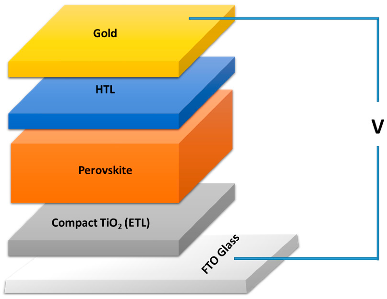
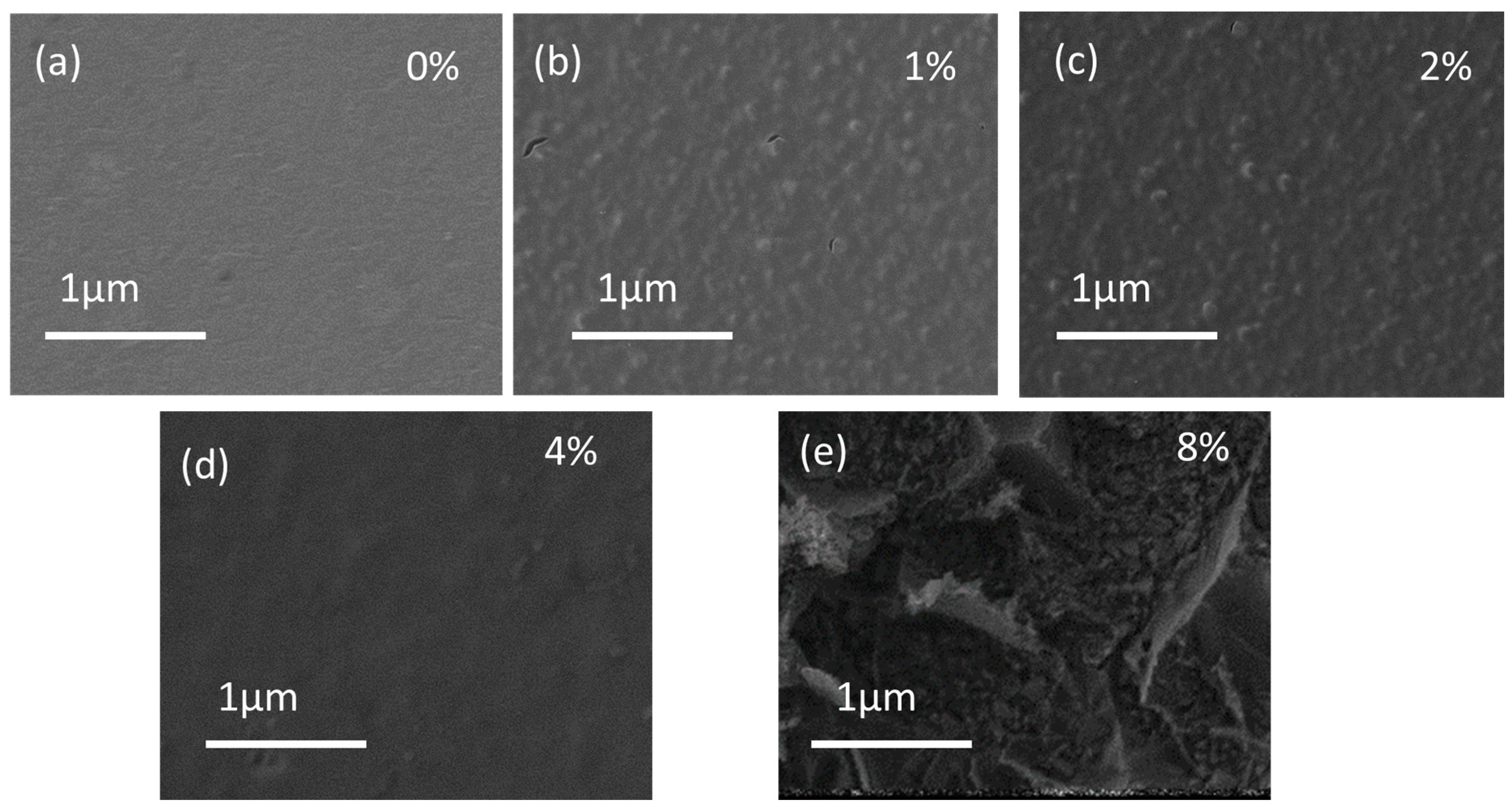
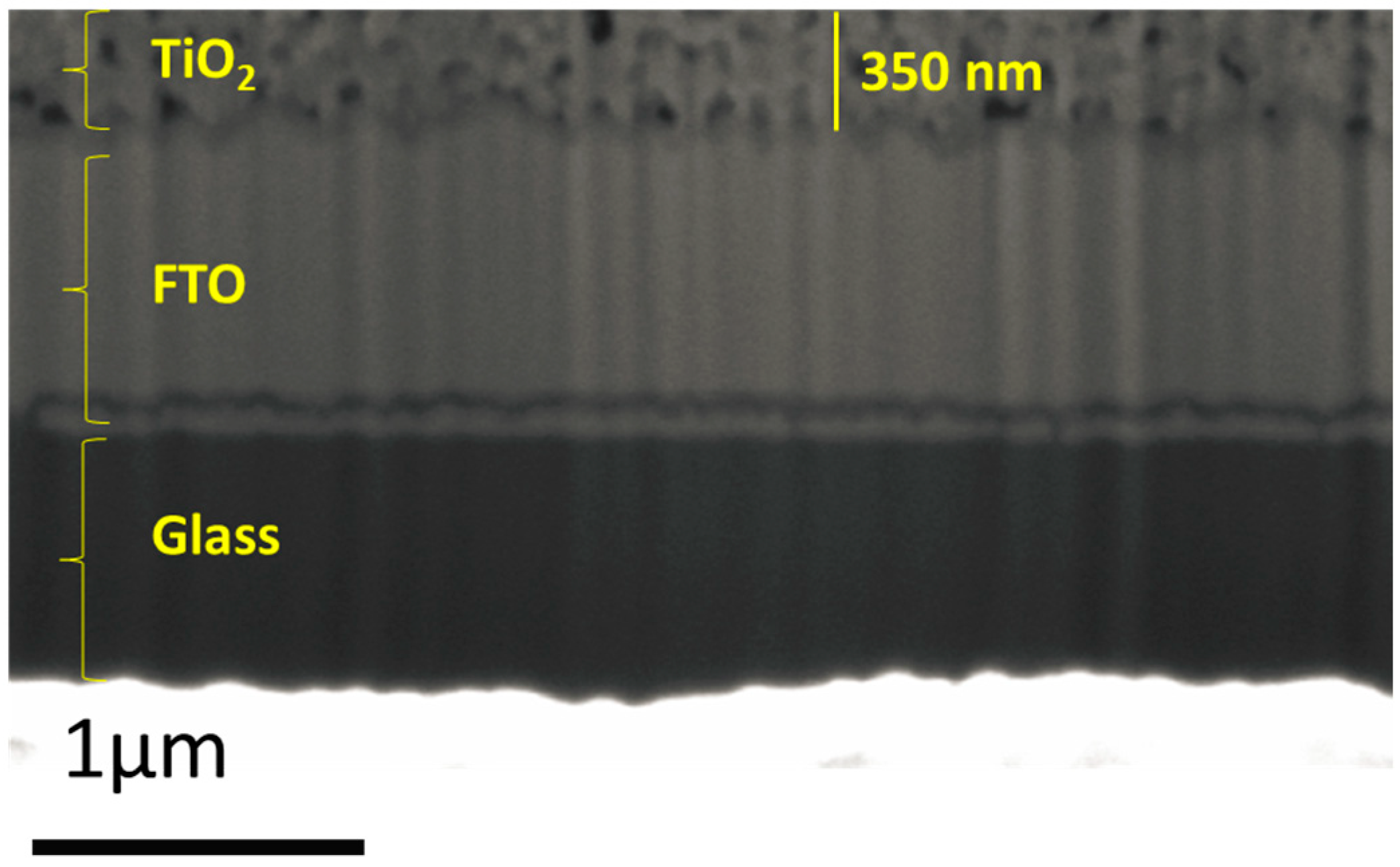
2.1. Morphological Properties

Figure 2 shows the SEM images of pure and doped TiO2. The TiO2 thin films demonstrate small spherical nanoparticles at a range of 200–500 nm that are orderly dispersed on the surface of the FTO glass to form a homogenous film. It seems that the addition of copper dopant to the TiO2 nanoparticles has no effect on the morphology of the TiO2 nanoparticles; all films depict a granular nanostructure, and with the increase in dopant concentration percentage, some regions show a microstructural defect with the presence of bumps and holes.
Figure 3 shows the cross-sectional SEM image of the TiO2 thin films with a thickness of 350 nm deposited on FTO glass. The thickness of the sample remains the same since the deposition parameters of the spin coating were sustained with same speed, solution quantity and duration. Moreover, the thickness seems to range between 340 and 380 nm for the different dopant concentrations.

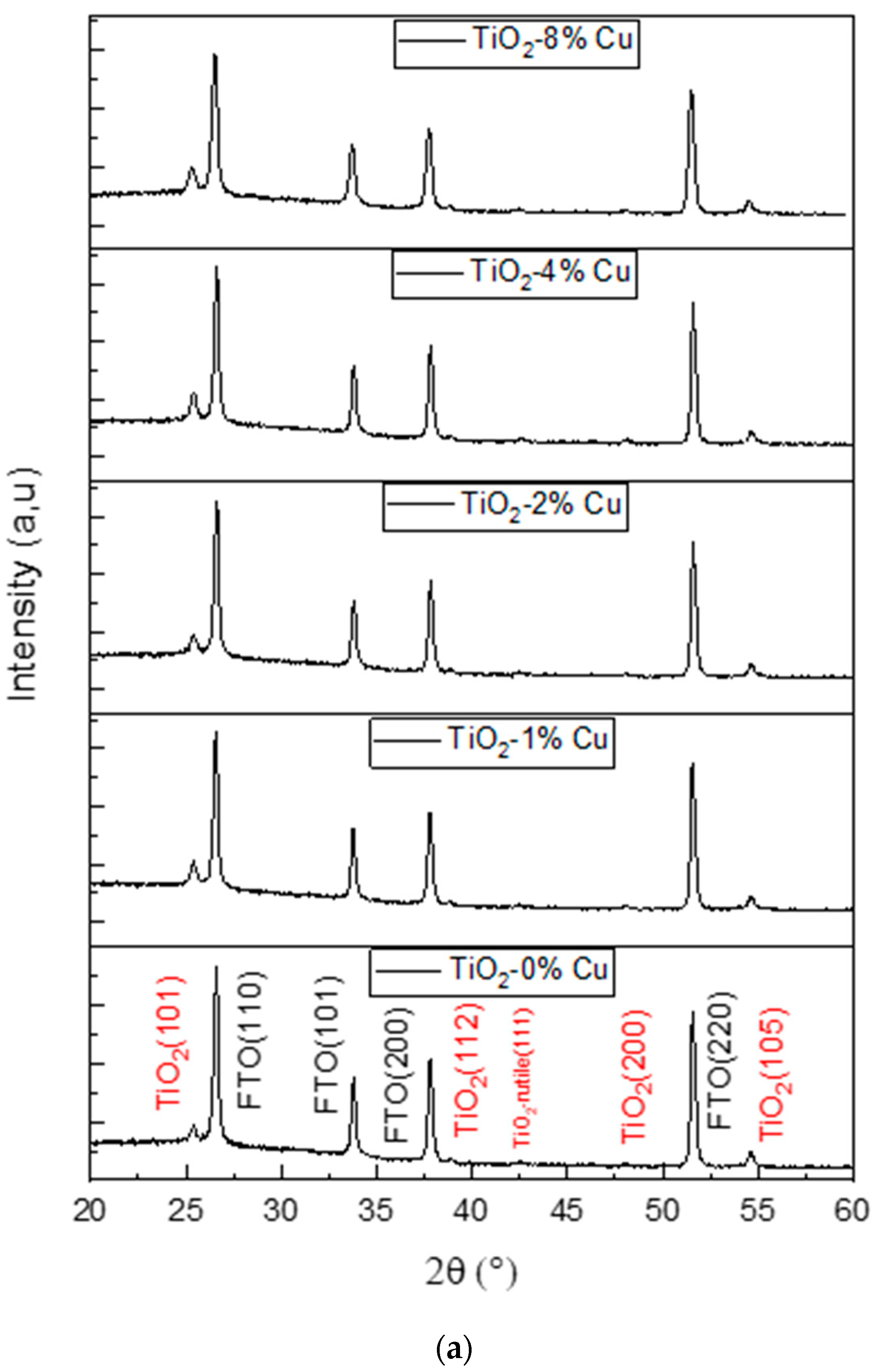
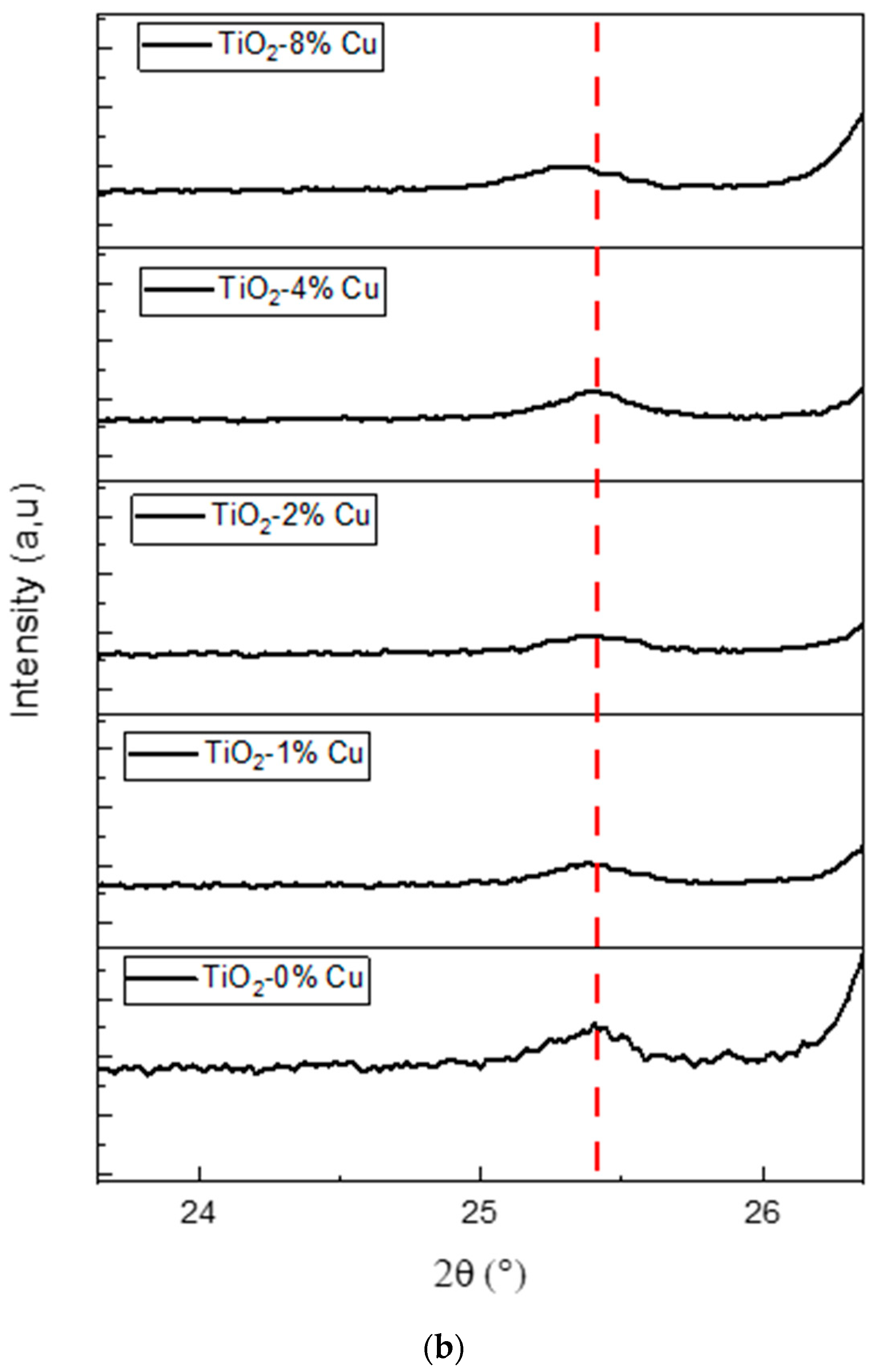
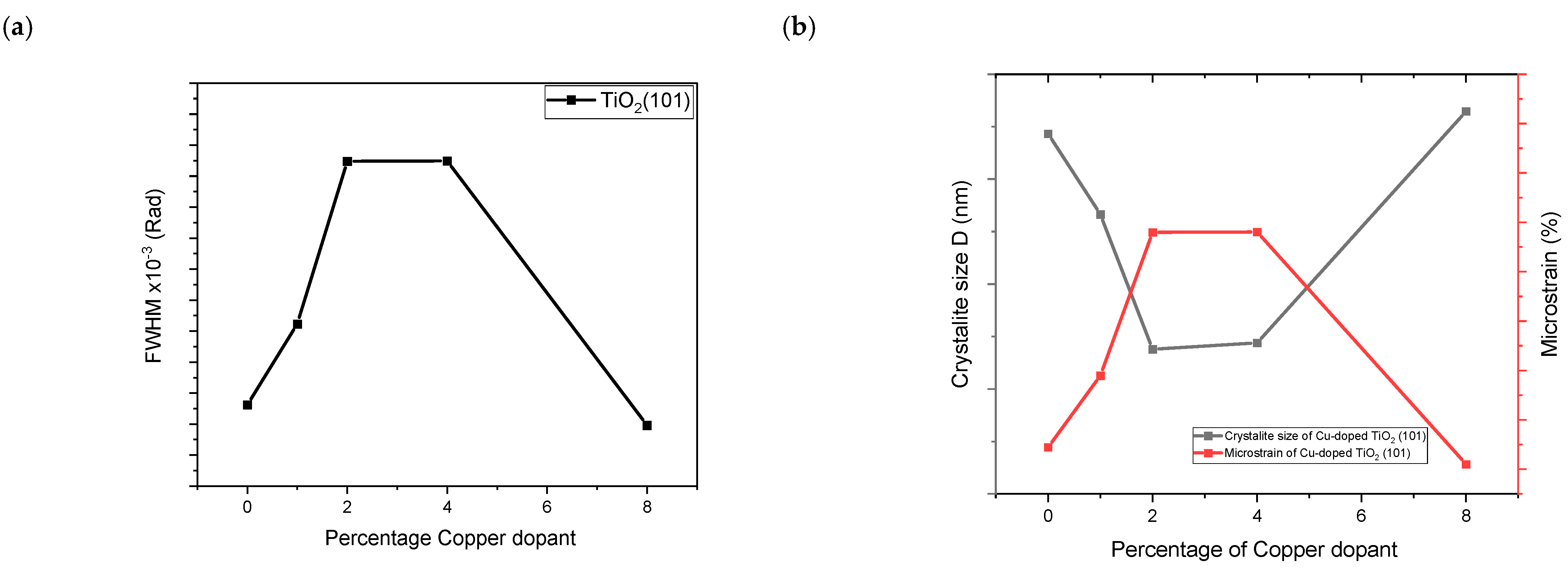
2.2. Structural Properties

The X-ray diffraction can provide information about the structural properties of the as-prepared samples. Figure 4a depicts a diffractogram with the visible crystalline patterns of undoped and Cu-doped TiO2 nanoparticles deposited on FTO glass with a preferred orientation at 2ϴ = 25.389° that correspond to anatase TiO2 (101), according to the reference card (JCPDS Card 21-1272) [40], and a small peak, with the other intense peaks corresponding to FTO glass (110), (101), (200) and (211); however, no Cu-related peaks were observable, which could mean the substitution with the Cu ion was successfully carried out without interstitial growth [41]. Moreover, the intensity of the anatase (101) peak increases with the increase in the dopant percentages. This could be due to the high incorporation of copper into the TiO2 structure, which in turn induces physical stressing on the lattice. From the used precursors, we can confirm the formation of Cu2+ in the solution and according to the literature the ionic radius of Cu2+ is (86 pm) and Ti4+ is (74.5 pm) [42]. According to Figure 4b, it seems that as we increase the percentage of the dopant the TiO2 (101) peak vaguely shifts to lower angles, especially for 8% sample. This could be better interpreted by the calculation of the crystallite size, lattice strain and microstrain, which are presented below.
The Scherrer equation for crystallite size and lattice strain determination is [43]
D = K λ β cos θ
1 D
The Wilson equation for microstrain determination is [43]
ε = β 4 t a n ( θ )
According to Figure 5 and the calculation in Table 1, it seems that the crystallite size is at its lowest values for the 2% and 4% samples and according to proportionality these samples also exhibits a high lattice strain and microstrain, which provides information on the degree of distortion, dislocations and defects present in the crystalline lattice; this could affect the photosensitivity of TiO2 nanoparticle thin films by inducing the density of charge carriers [44].

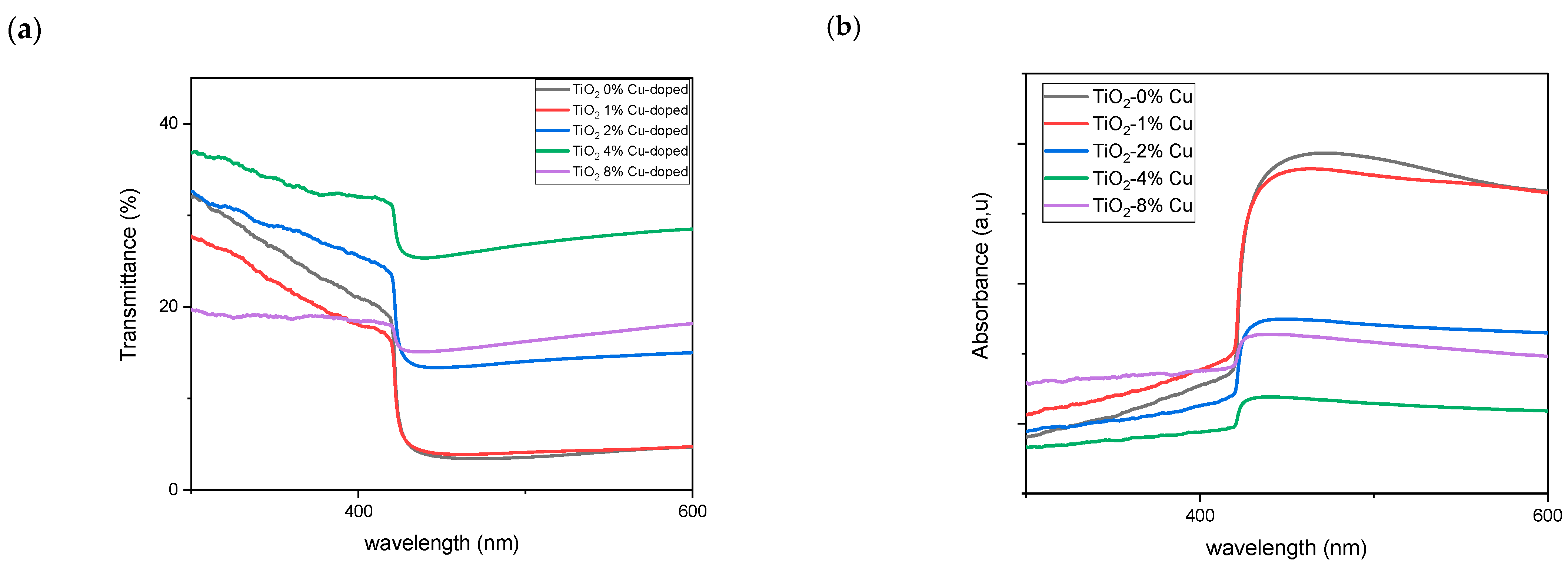
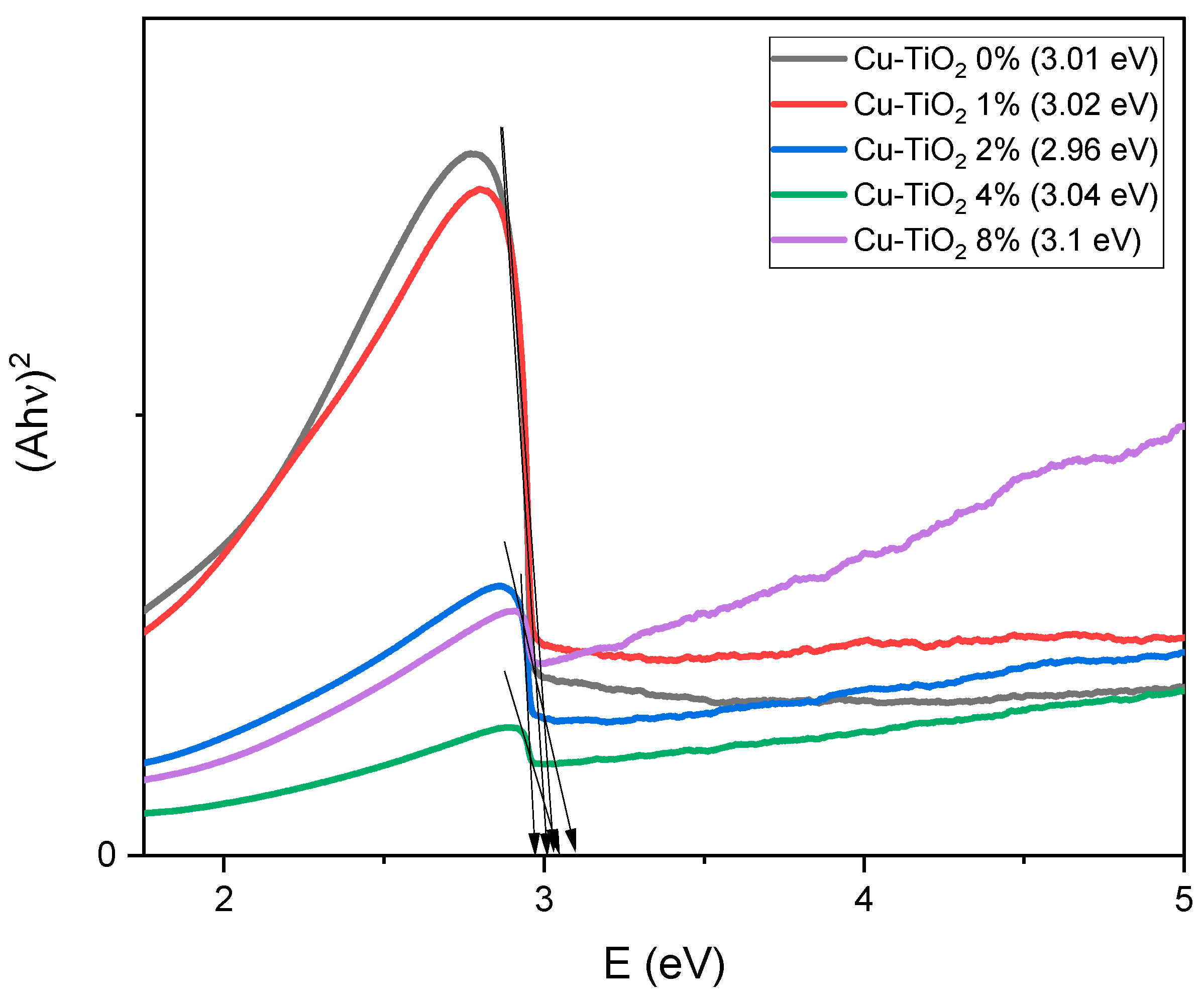
2.3. Optical Properties

To acknowledge the effect of Cu doping on the optical properties of the TiO2 nanoparticle thin film, we used UV–Vis spectroscopy and obtained transmittance and absorbance spectra (Figure 6). Figure 6a depicts the transmittance of each sample, and it seems that the 4% copper dopant TiO2 presents more light transmission than the other samples, followed by the 2% copper dopant TiO2; this could positively affect the charge mobility and the performance of TiO2 as an electron transport layer [45]. Figure 6b shows the absorption spectra of the samples, and it seems that at the range 300–400 nm, the sample with 8% copper dopant has a high absorbance value compared to the other samples; as for the 2% and 4% samples, they have a low absorbance value, even lower than the undoped TiO2, but unexpectedly the 1% sample presents a higher light absorption than the undoped and 2% and 4% Cu-doped TiO2.
To better understand the effect of doping with copper on the optical band gap of the samples, we used the Tauc formula below [46]
(Ahʋ)1/n = C(hʋ − Eg)
where A is the absorption coefficient, C is a constant, Eg is the average band gap of the material and n depends on the type of the transition. After examination of the obtained Tauc plots (Ahʋ)2 vs. hʋ (Figure 7), the difference in the optical band gap is clear. If we exclude the 2% sample, it is noticeable that by increasing the copper doping percentage (the concentration of dopant) the optical band gap increases from 3.01 eV for undoped TiO2 to 3.1 eV for 8% copper-doped TiO2. But it is obvious to state that the optical band gap for the sample of 2% Cu-doped TiO2 decreases in comparison with undoped and the other doped samples to a value of 2.96 eV. This is in accordance with Nair et al., who studied the effect of doping and crystalline properties on the band gap of nanoparticles and concluded that clearly there is a correlation between the particle size, strain and band gap [47]. Considering the calculated values in Table 1 and the obtained results from the Figure 5, the 2% Cu-doped TiO2 nanoparticle sample presents the lowest crystallite size, the highest microstrain and the lowest bang gap. So, in short, and as they reported, when the particle is extremely small, pressure surface increases, meaning lattice strain increases and thus the band gap decreases [48]. So, as reported, Red shift or a decrease in optical band gap with a decrease in particle size arises due to the surface and interface effect and Blue shift or an increase in energy is due to the quantum size effect, which is the case for 1%, 4% and 8% copper-doped TiO2.

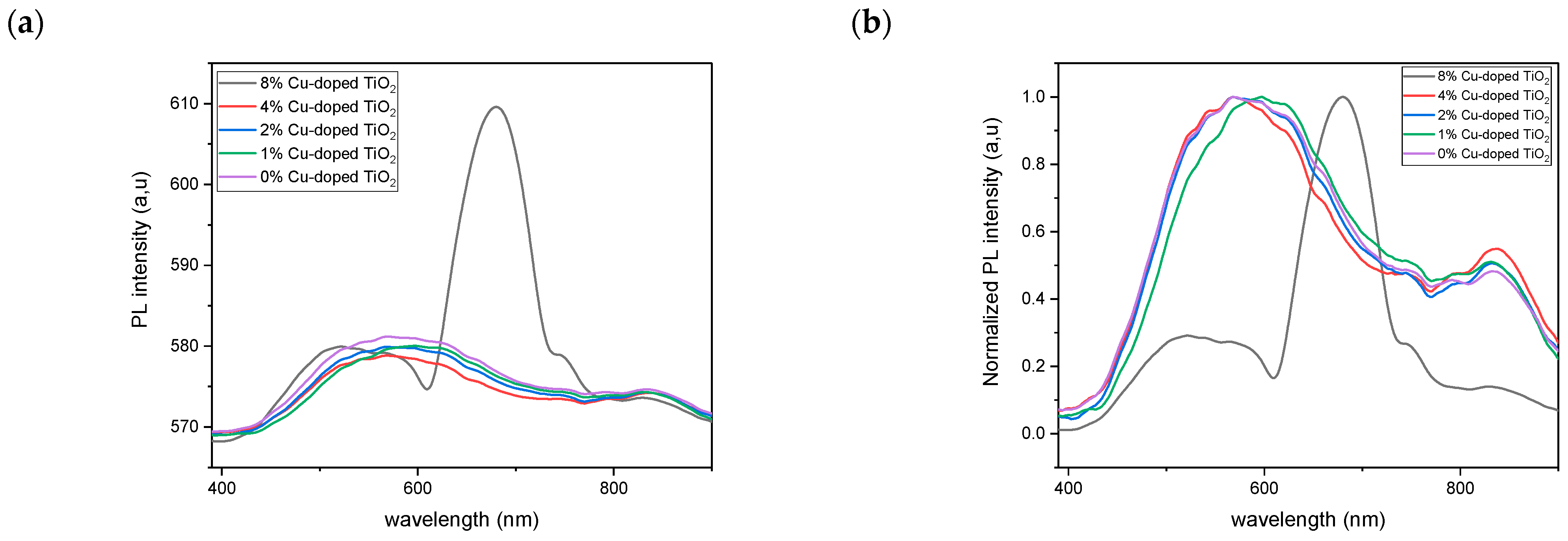
2.4. Photoluminescence

We investigated the recombination of charge carriers for undoped and Cu-doped TiO2 nanoparticles. All samples were optically characterized with photoluminescence spectroscopy. As Figure 8 depicts, TiO2 nanoparticles are not photoluminescent, since the PL spectra did not show any peak around the absorption wavelength that corresponds to the calculated band gap ranging from 2.96 to 3.1 eV (420–401 nm). The observed peak collection between 450 and 700 nm is related to the oxygen vacancies in the TiO2 structure [49]. The peak appears to be decreasing with the increase in dopant concentration, which means a decrease in the recombination rate of charge carriers e/h+, hence fast electronic transport and better photoactivity, except for the 8% and 2% samples, which give a higher PL intensity which could be due the high formation of defects, while the 4% sample presents the lowest PL intensity; also, it is clear that the doped samples present the same spectra shape as the undoped one, which means that Cu doping does not induce any PL signals. The significant peak of the 8% Cu-doped TiO2 nanoparticles at 780 nm corresponds to the band gap of CuO (1.6 eV) according to the literature. But this hypothesis cannot be right since the XRD analysis did not show any peaks related to copper oxide structure, unless it also means that the formed copper oxide nanoparticles are extremely well dispersed on TiO2 nanoparticles and that is why they are undetectable by the X-ray diffractometer.

3. Experimental Details Materials and Methods

3.1. Materials

All chemicals and reagents were used directly without further purification as received. Absolute ethanol, isopropyl alcohol, acetone, FTO, Titanium diisopropoxide bis(acetylacetonante) 75 wt.% in isopropanol (C16H32O6Ti) and Cupric Acetate Monohydrate (Copper (II) Acetate Monohydrate) pure, 98% (C4H8CuO5). All the products were bought from Sigma-Aldrich (St. Louis, MO, USA).

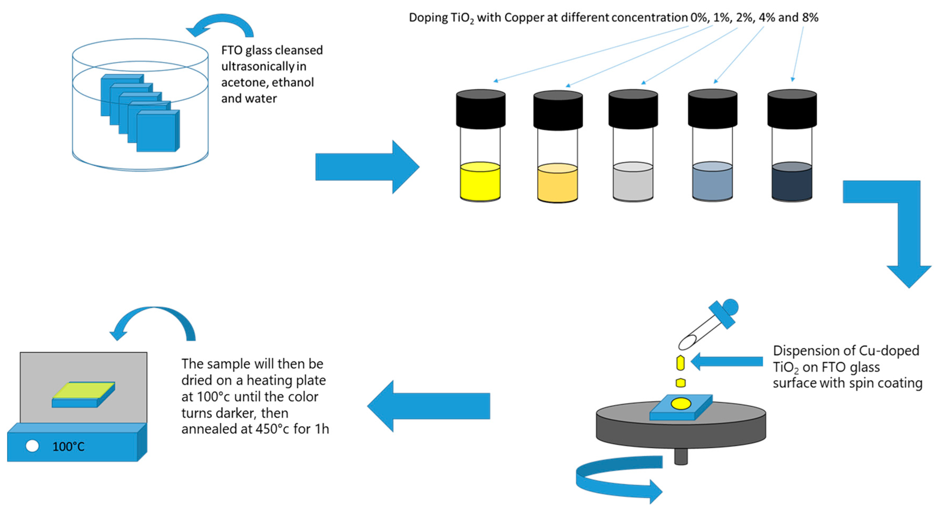
3.2. Pure and Cu-Doped TiO2 Film Elaboration

Firstly, the FTO glass was cleaned with acetone, ethanol and distilled water. Then, to deposit the TiO2 nanoparticles on the surface of the FTO glass, a simple cost-free method was used: spin coating, which consists of coating the FTO glass surface with a solution of titanium precursor. To study the effect of doping, we added a portion of copper precursor, while varying the amount of copper from 0%, 1%, 2%, 4% to 8%. After the deposition of the Cu dopant TiO2 thin film with spin coating, the as-prepared samples were annealed at 450 °C for 1 h and then naturally cooled down for morphological, structural and optical characterization. All of the steps are illustrated in Figure 9.

3.3. Characterization Techniques

The samples were morphologically characterized using scanning electron microscopy (SEM, FEI XL30 ESEM Company, Hillsboro, OR, USA). As for the structural stability and crystallographic formation of the phase, X-ray diffraction (XRD) was performed using a Philips X’PERT-MPD diffractometer equipped with CuKα radiation (λ = 1.5406 Å), with the diffraction patterns in the range of 20–80°. To determine the gap energy of each sample and its transmittance and absorbance properties, we used a UV–Vis spectrophotometer and photoluminescence (PL) spectroscopy in the range of 200 and 1200 nm by equipping a PerkinElmer Lambda 950.

4. Conclusions

TiO2 nanoparticles doped with copper were synthesized with a simple method of spin coating, which consists of dispersing the prepared solution on FTO glass at high speed, and these samples of Cu-doped TiO2 at 0%, 1%, 2%, 4% and 8% were characterized morphologically, structurally and optically and the acquired results reveal that the 4% sample has the highest transmittance, while the 2% is the second highest; these samples could be perfect candidates for electron transport. The 2% sample exhibited the lowest band gap energy of 2.96 eV, whereas the 8% samples exhibit the highest at 3.05 eV; the 8% sample also showed a new PL peak compared to the other samples, which could be related to the copper oxide.

Author Contributions

Conceptualization, A.H. and B.B.; Methodology, L.K.; Software, S.S. and L.K.; Validation, A.B. and B.M.S.; Formal analysis, S.S. and L.K.; Investigation, A.B.; Resources, B.B.; Data curation, S.S.; Writing—original draft, S.S.; Writing—review & editing, A.B., A.H., L.K. and B.M.S.; Visualization, A.B.; Supervision, A.H., B.B. and B.M.S.; Funding acquisition, B.B. and B.M.S. All authors have read and agreed to the published version of the manuscript.

Funding

Syrine Sassi acknowledged Erasmus plus for the grant, the author Amal Bouich acknowledges MCIN for funding support through MS Fellowship (MCIN/AEI/10.13039/501100011033) and UE NextGeneration. This research was funded by the Ministerio de Ciencia e Innovación (Spain) and by the Spanish Agencia Estatal de Investigación through projects BESTMAT PID2019-107137RB-C21/AEI/10.13039/5011000 11033 and PID2019-107137RB-C22/AEI/10.13039/501100011033 and by ERDF under the funding “A way of making Europe”.

Data Availability Statement

The original contributions presented in the study are included in the article, further inquiries can be directed to the corresponding authors.

Conflicts of Interest

The authors declare no conflict of interest.

References

  1. Hsu, A.; Rosengarten, C.; Weinfurter, A.; Xie, Y. Renewable Energy and Energy Efficiency in Developing Countries: Contributions to Reducing Global Emissions; United Nations Environment Programme: New York, NY, USA, 2017. [Google Scholar]
  2. Green, M.A.; Emery, K.; Hishikawa, Y.; Warta, W.; Dunlop, E.D. Solar cell efficiency tables (Version 45). Prog. Photovolt. Res. Appl. 2015, 23, 1–9. [Google Scholar] [CrossRef]
  3. Saïdi, H.; Boujmil, M.F.; Durand, B.; Lazzari, J.L.; Bouaïcha, M. Elaboration and characterization of CuInSe2 thin films using one-step electrodeposition method on silicon substrate for photovoltaic application. Mater. Res. Express 2018, 5, 016414. [Google Scholar] [CrossRef]
  4. Rathore, N.; Panwar, N.L.; Yettou, F.; Gama, A. A comprehensive review of different types of solar photovoltaic cells and their applications. Int. J. Ambient. Energy 2021, 42, 1200–1217. [Google Scholar] [CrossRef]
  5. Dong, Y.; Yang, Y.; Qiu, L.; Dong, G.; Xia, D.; Liu, X.; Li, M.; Fan, R. Polyoxometalate-Based Inorganic-Organic Hybrid [Cu(phen)2]2[(α-Mo8O26)]: A New Additive to Spiro-OMeTAD for Efficient and Stable Perovskite Solar Cells. ACS Appl. Energy Mater. 2019, 2, 4224–4233. [Google Scholar] [CrossRef]
  6. Wu, M.C.; Chan, S.H.; Lee, K.M.; Chen, S.H.; Jao, M.H.; Chen, Y.F.; Su, W.F. Enhancing the efficiency of perovskite solar cells using mesoscopic zinc-doped TiO2 as the electron extraction layer through band alignment. Mater. Chem. A 2018, 6, 16920–16931. [Google Scholar] [CrossRef]
  7. Teimouri, R.; Heydari, Z.; Ghaziani, M.P.; Madani, M.; Abdy, H.; Kolahdouz, M.; Asl-Soleimani, E. Synthesizing Li doped TiO2 electron transport layers for highly efficient planar perovskite solar cell. Superlattices Microstruct. 2020, 145, 106627. [Google Scholar] [CrossRef]
  8. Mohammad, A.; Mahjabeen, F. Promises and Challenges of Perovskite Solar Cells: A Comprehensive Review. BULLET J. Multidisiplin. Ilmu 2023, 2, 1147–1157. [Google Scholar]
  9. Ma, T.; Wang, S.; Zhang, Y.; Zhang, K. Yi, The development of all-inorganic CsPbX3 perovskite solar cells. J. Mater. Sci. 2020, 55, 464–479. [Google Scholar] [CrossRef]
  10. Bouich, A.; Torres, J.C.; Khattak, Y.H.; Baig, F.; Marí-Guaita, J.; Soucase, B.M.; Mendez-Blas, A.; Palacios, P. Bright future by controlling α/δ phase junction of formamidinium lead iodide doped by imidazolium for solar cells: Insight from experimental, DFT calculations and SCAPS simulation. Surf. Interfaces 2023, 40, 103159. [Google Scholar] [CrossRef]
  11. Ding, M.; Sun, L.; Chen, X.; Luo, T.; Ye, T.; Zhao, C.; Zhang, W.; Chang, H. Airprocessed, large grain perovskite films with low trap density from perovskite crystal engineering for high-performance perovskite solar cells with improved ambient stability. J. Mater. Sci. 2019, 54, 12000–12011. [Google Scholar] [CrossRef]
  12. Bouich, A.; Marí-Guaita, J.; Soucase, B.M.; Palacios, P. Bright future by enhancing the stability of methylammonium lead triiodideperovskites thin films through Rb, Cs and Li as dopants. Mater. Res. Bull. 2023, 163, 112213. [Google Scholar] [CrossRef]
  13. Hossain, M.K.; Samajdar, D.P.; Das, R.C.; Arnab, A.A.; Rahman, M.F.; Rubel, M.H.; Islam, M.R.; Bencherif, H.; Pandey, R.; Madan, J.; et al. Design and simulation of Cs2BiAgI6 double perovskite solar cells with different electron transport layers for efficiency enhancement. Energy Fuels 2023, 37, 3957–3979. [Google Scholar] [CrossRef]
  14. Mukametkali, T.M.; Ilyassov, B.R.; Aimukhanov, A.K.; Serikov, T.M.; Baltabekov, A.S.; Aldasheva, L.S.; Zeinidenov, A.K. Effect of the TiO2 electron transport layer thickness on charge transfer processes in perovskite solar cells. Phys. B Condens. Matter 2023, 659, 414784. [Google Scholar] [CrossRef]
  15. Cheng, M.; Zuo, C.; Wu, Y.; Li, Z.; Xu, B.; Hua, Y.; Ding, L. Charge-transport layer engineering in perovskite solar cells. Sci. Bull. 2020, 65, 1237–1241. [Google Scholar] [CrossRef] [PubMed]
  16. Lin, L.; Jones, T.W.; Yang, T.C.; Duffy, N.W.; Li, J.; Zhao, L.; Chi, B.; Wang, X.; Wilson, G.J. Inorganic electron transport materials in perovskite solar cells. Adv. Funct. Mater. 2021, 31, 2008300. [Google Scholar] [CrossRef]
  17. Li, F.; Shen, Z.; Weng, Y.; Lou, Q.; Chen, C.; Shen, L.; Guo, W.; Li, G. Novel electron transport layer material for perovskite solar cells with over 22% efficiency and long-term stability. Adv. Funct. Mater. 2020, 30, 2004933. [Google Scholar] [CrossRef]
  18. Valadi, K.; Gharibi, S.; Taheri-Ledari, R.; Akin, S.; Maleki, A.; Shalan, A.E. Metal oxide electron transport materials for perovskite solar cells: A review. Environ. Chem. Lett. 2021, 19, 2185–2207. [Google Scholar] [CrossRef]
  19. Zhen, C.; Wu, T.; Chen, R.; Wang, L.; Liu, G.; Cheng, H.M. Strategies for Modifying TiO2 Based Electron Transport Layers to Boost Perovskite Solar Cells. ACS Sustain. Chem. Eng. 2019, 7, 4586–4618. [Google Scholar] [CrossRef]
  20. Kaewprajak, A.; Kumnorkaew, P.; Lohawet, K.; Duong, B.; Chonsut, T.; Kayunkid, N.; Saranrom, N.; Promarak, V. An unconventional blade coating for low-cost fabrication of PCDTBT: PC70BM polymer and CH3NH3PbIxCl3-x perovskite solar cells. Surf. Interfaces 2021, 23, 100969. [Google Scholar] [CrossRef]
  21. Stranks, S.D.; Eperon, G.E.; Grancini, G.; Menelaou, C.; Alcocer, M.J.; Leijtens, T.; Herz, L.M.; Petrozza, A.; Snaith, H.J. Electron-hole diffusion lengths exceeding 1 micrometer in an organometal trihalide perovskite absorber. Science 2013, 342, 341–344. [Google Scholar] [CrossRef]
  22. Nishat, S.S.; Hossain, M.J.; Mullick, F.E.; Kabir, A.; Chowdhury, S.; Islam, S.; Hossain, M. Performance analysis of perovskite solar cells using DFT-extracted parameters of metal-doped TiO2 electron transport layer. J. Phys. Chem. C 2021, 125, 13158–13166. [Google Scholar] [CrossRef]
  23. Che Halin, D.S.; Azhari, A.W.; Mohd Salleh, M.A.; Muhammad Nadzri, N.I.; Vizureanu, P.; Abdullah, M.M.; Wahab, J.A.; Sandu, A.V. Metal-Doped TiO2 Thin Film as an Electron Transfer Layer for Perovskite Solar Cells: A Review. Coatings 2022, 13, 4. [Google Scholar] [CrossRef]
  24. Chen, S.H.; Ho, C.M.; Chang, Y.H.; Lee, K.M.; Wu, M.C. Efficient perovskite solar cells with low J-V hysteretic behavior based on mesoporous Sn-doped TiO2 electron extraction layer. Chem. Eng. J. 2022, 445, 136761. [Google Scholar] [CrossRef]
  25. Chen, S.H.; Chan, S.H.; Lin, Y.T.; Wu, M.C. Enhanced power conversion efficiency of perovskite solar cells based on mesoscopic Ag-doped TiO2 electron transport layer. Appl. Surf. Sci. 2019, 469, 18–26. [Google Scholar]
  26. Dahlan, D.; Saad, S.K.; Berli, A.U.; Bajili, A.; Umar, A.A. Synthesis of two-dimensional nanowall of Cu-Doped TiO2 and its application as photoanode in DSSCs. Phys. E Low-Dimens. Syst. Nanostructures 2017, 91, 185–189. [Google Scholar] [CrossRef]
  27. Abbas, M.M.; Rasheed, M. Investigation of structural, Mechanical, Thermal and Optical Properties of Cu Doped TiO2. Iraqi J. Phys. 2021, 19, 1–9. [Google Scholar] [CrossRef]
  28. Bhattacharyya, K.; Mane, G.P.; Rane, V.; Tripathi, A.K.; Tyagi, A.K. Selective CO2 photoreduction with Cu-doped TiO2 photocatalyst: Delineating the crucial role of Cu-oxidation state and oxygen vacancies. J. Phys. Chem. C 2021, 125, 1793–1810. [Google Scholar] [CrossRef]
  29. Dhonde, M.; Sahu, K.; Murty, V.V. Cu-doped TiO2 nanoparticles/graphene composites for efficient dye-sensitized solar cells. Sol. Energy 2021, 220, 418–424. [Google Scholar] [CrossRef]
  30. Deng, Z.; Li, L.; Ren, Y.; Ma, C.; Liang, J.; Dong, K.; Liu, Q.; Luo, Y.; Li, T.; Tang, B.; et al. Highly efficient two-electron electroreduction of oxygen into hydrogen peroxide over Cu-doped TiO2. Nano Res. 2022, 15, 3880–3885. [Google Scholar] [CrossRef]
  31. Raguram, T.; Rajni, K.S. Synthesis and characterisation of Cu-Doped TiO2 nanoparticles for DSSC and photocatalytic applications. Int. J. Hydrog. Energy 2022, 47, 4674–4689. [Google Scholar] [CrossRef]
  32. He, Z.; Zhang, S.; Yin, L.; Hayat, M.D.; Cao, P. Cu–TiO2 nanocomposite coatings prepared from sol-enhanced electrodeposition. Int. J. Mod. Phys. B 2020, 34, 2040038. [Google Scholar] [CrossRef]
  33. Reda, S.M.; Khairy, M.; Mousa, M.A. Photocatalytic activity of nitrogen and copper doped TiO2 nanoparticles prepared by microwave-assisted sol-gel process. Arab. J. Chem. 2020, 13, 86–95. [Google Scholar] [CrossRef]
  34. Farzaneh, A.; Javidani, M.; Esrafili, M.D.; Mermer, O. Optical and photocatalytic characteristics of Al and Cu doped TiO2: Experimental assessments and DFT calculations. J. Phys. Chem. Solids 2022, 161, 110404. [Google Scholar] [CrossRef]
  35. Sahu, K.; Dhonde, M.; Murty, V.V. Microwave-assisted hydrothermal synthesis of Cu-doped TiO2 nanoparticles for efficient dye-sensitized solar cell with improved open-circuit voltage. Int. J. Energy Res. 2021, 45, 5423–5432. [Google Scholar] [CrossRef]
  36. Jasima, F.H.; Shakirb, H.R.; Chiada, S.S.; Habubic, N.F.; Mosad, Z.S.; Kadhime, Y.H.; Jadanf, M. Characterizations of sprayed TiO2 and Cu doped TiO2 thin films prepared by spray pyrolysis method. Dig. J. Nanomater. Biostructures (DJNB) 2023, 18, 1385–1393. [Google Scholar] [CrossRef]
  37. Lukong, V.T.; Ukoba, K.; Jen, T.C. Review of self-cleaning TiO2 thin films deposited with spin coating. Int. J. Adv. Manuf. Technol. 2022, 122, 3525–3546. [Google Scholar] [CrossRef]
  38. Liu, J.; Yang, Z.; Gong, Z.; Shen, Z.; Ye, Y.; Yang, B.; Qiu, Y.; Ye, B.; Xu, L.; Guo, T.; et al. Weak light-stimulated synaptic hybrid phototransistors based on islandlike perovskite films prepared by spin coating. ACS Appl. Mater. Interfaces 2021, 13, 13362–13371. [Google Scholar] [CrossRef]
  39. Liao, Y.H.; Chang, Y.H.; Lin, T.H.; Chan, S.H.; Lee, K.M.; Hsu, K.H.; Hsu, J.F.; Wu, M.C. Boosting the power conversion efficiency of perovskite solar cells based on Sn doped TiO2 electron extraction layer via modification the TiO2 phase junction. Sol. Energy 2020, 205, 390–398. [Google Scholar] [CrossRef]
  40. Hajjaji, M.A.; Missaoui, K.; Trabelsi, K.; Bouzaza, A.; Bessais, B.; Hajjaji, A.; Assadi, A.A. Electrodeposited Platinum Nanoparticles on Highly Ordered Titanium Dioxide Nanotubes for Photocatalytic Application: Enhancement of Photocatalytic Degradation of Amido Black Dye. Catal. Lett. 2023, 154, 1242–1254. [Google Scholar] [CrossRef]
  41. Nguyen, T.M.; Bark, C.W. Synthesis of Cobalt-Doped TiO2 Based on Metal-Organic Frameworks as an Effective Electron Transport Material in Perovskite Solar Cells. ACS Omega 2020, 5, 2280–2286. [Google Scholar] [CrossRef] [PubMed]
  42. Bensouici, F.; Bououdina, M.; Dakhel, A.A.; Tala-Ighil, R.; Tounane, M.; Iratni, A.; Souier, T.; Liu, S.; Cai, W.J. Optical, structural and photocatalysis properties of Cu-doped TiO2 thin films. J. Appl. Sci. 2017, 395, 110–116. [Google Scholar]
  43. Sassi, S.; Trabelsi, K.; El Jery, A.; Abidi, M.; Hajjaji, A.; Khezami, L.; Karrech, A.; Gaidi, M.; Soucase, B.M.; Bessais, B. Synergistic effect of CuxOy-NPs/TiO2-NTs heterostructure on the photodegradation of amido black staining. Optik 2023, 272, 170234. [Google Scholar] [CrossRef]
  44. Trabelsi, K.; Jemai, S.; El Jery, A.; Sassi, S.; Guesmi, A.; Khezami, L.; Hajjaji, A.; Gaidi, M.; Bessais, B. Ag-NPs coating influence on TiO2-NTs photocatalytic performances on Amido Black staining. Res. Sq. 2022. [Google Scholar] [CrossRef]
  45. Sławek, A.; Starowicz, Z.; Lipiński, M. The influence of the thickness of compact TiO2 electron transport layer on the performance of planar CH3NH3PbI3 perovskite solar cells. Materials 2021, 14, 3295. [Google Scholar] [CrossRef]
  46. Bouich, A.; Torres, J.C.; Chfii, H.; Marí-Guaita, J.; Khattak, Y.H.; Baig, F.; Soucase, B.M.; Palacios, P. Delafossite as hole transport layer a new pathway for efficient perovskite-based solar cells: Insight from experimental, DFT and numerical analysis. Sol. Energy 2023, 250, 18–32. [Google Scholar] [CrossRef]
  47. Nair, S.S.; Mathews, M.; Anantharaman, M.R. Anantharaman. Evidence for blueshift by weak exciton confinement and tuning of bandgap in superparamagnetic nanocomposites. Chem. Phys. Lett. 2005, 406, 398–403. [Google Scholar] [CrossRef]
  48. Deotale, A.J.; Nandedkar, R.V. Correlation between particle size, strain and band gap of iron oxide nanoparticles. Mater. Today Proc. 2016, 3, 2069–2076. [Google Scholar] [CrossRef]
  49. Komaraiah, D.; Radha, E.; Kalarikkal, N.; Sivakumar, J.; Reddy, M.R.; Sayanna, R. Structural, optical and photoluminescence studies of sol-gel synthesized pure and iron doped TiO2 photocatalysts. Ceram. Int. 2019, 45, 25060–25068. [Google Scholar] [CrossRef]
Figure 1. Schematic of perovskite solar cell.
Inorganics 12 00188 g001
Figure 2. SEM images of the (a) undoped and (b) 1%, (c) 2%, (d) 4% and (e) 8% Cu-doped TiO2 nanoparticle thin films.
Inorganics 12 00188 g002
Figure 3. Cross-sectional SEM image of TiO2 thin films on FTO glass.
Inorganics 12 00188 g003
Figure 4. (a) XRD diffractogram of the undoped and 1%, 2%, 4% and 8% Cu-doped TiO2 nanoparticle thin films. (b) A close-up of the TiO2 (101) peak.
Inorganics 12 00188 g004aInorganics 12 00188 g004b
Figure 5. Variation in (a) FWHM and (b) crystallite size and microstrain of the undoped and 1%, 2%, 4% and 8% Cu-doped TiO2 nanoparticle thin films.
Inorganics 12 00188 g005
Figure 6. (a) Transmittance and (b) absorbance spectra of the undoped and 1%, 2%, 4% and 8% Cu-doped TiO2 nanoparticle thin films.
Inorganics 12 00188 g006
Figure 7. Tauc plots of the undoped and 1%, 2%, 4% and 8% Cu-doped TiO2 nanoparticle thin films.
Inorganics 12 00188 g007
Figure 8. (a) Photoluminescence and (b) normalized PL spectra of the undoped and 1%, 2%, 4% and 8% Cu-doped TiO2 nanoparticle thin films.
Inorganics 12 00188 g008
Figure 9. Illustration of the steps for sample preparation of 0%, 1%, 2%, 4% and 8% Cu-doped TiO2 nanoparticle thin films.
Inorganics 12 00188 g009
Table 1. Crystallite size, lattice strain and microstrain calculations of the undoped and 1%, 2%, 4% and 8% Cu-doped TiO2 at the preferred orientation (101).
Cu-Doped TiO2 (101)2ϴ (deg)d(101) (Å)FWHM (rad)D (nm)1/D (nm−1)Ԑ (%) × 10−3
0% Cu25.3893.5069340.00296247.160.02123.289
1% Cu25.3883.5155070.00322343.330.0233.579
2% Cu25.3973.4726650.00374836.90.02714.16
4% Cu25.403.5137340.00374937.20.02684.161
8% Cu25.323.5089710.00289648.230.02073.22
Disclaimer/Publisher’s Note: The statements, opinions and data contained in all publications are solely those of the individual author(s) and contributor(s) and not of MDPI and/or the editor(s). MDPI and/or the editor(s) disclaim responsibility for any injury to people or property resulting from any ideas, methods, instructions or products referred to in the content.

