
Promoted Formation of Photoactive α-Formamidinium Cesium Lead Triiodide Perovskite Crystals by Germanium Addition


Abstract
:1. Introduction
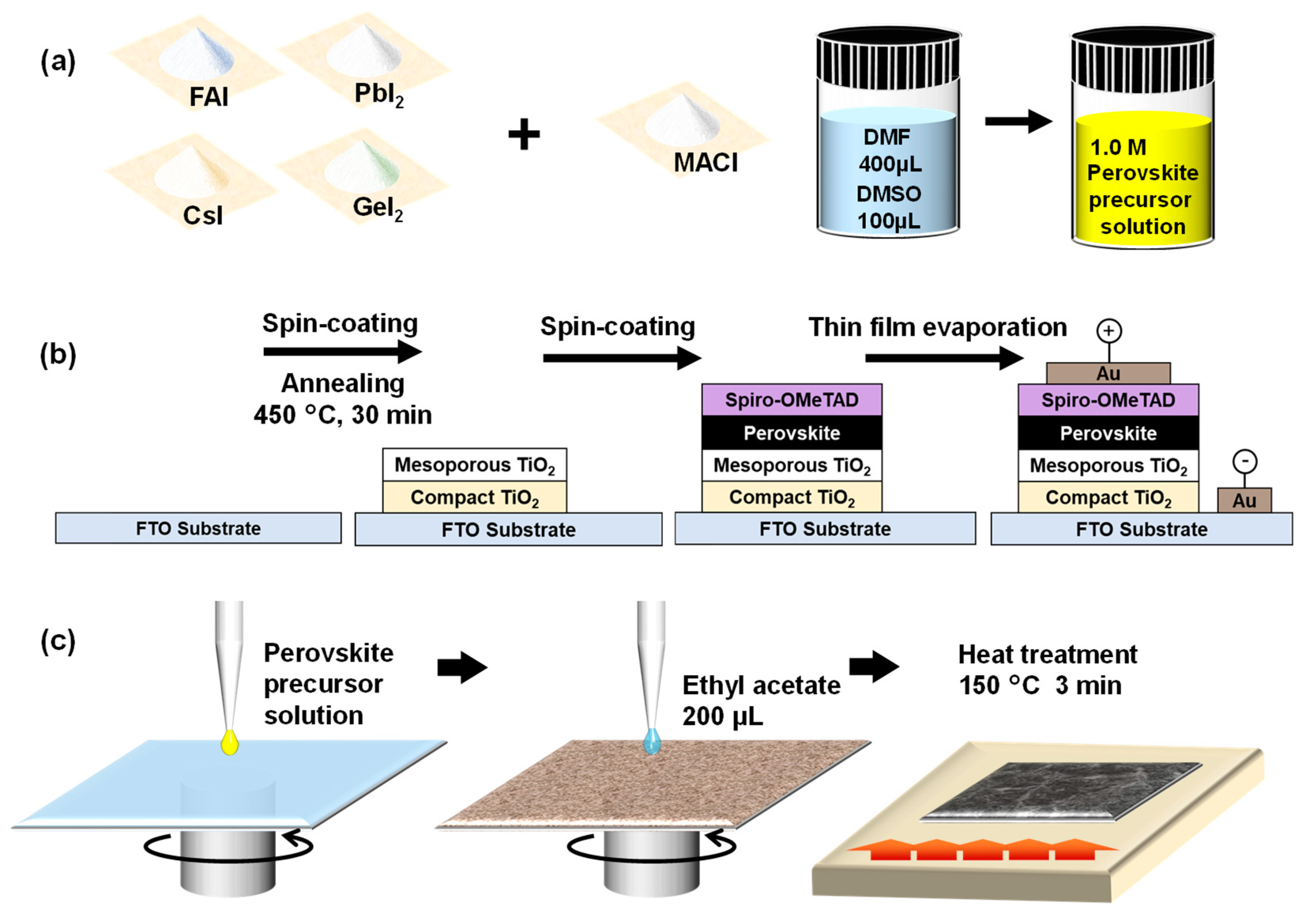
2. Experimental Procedures
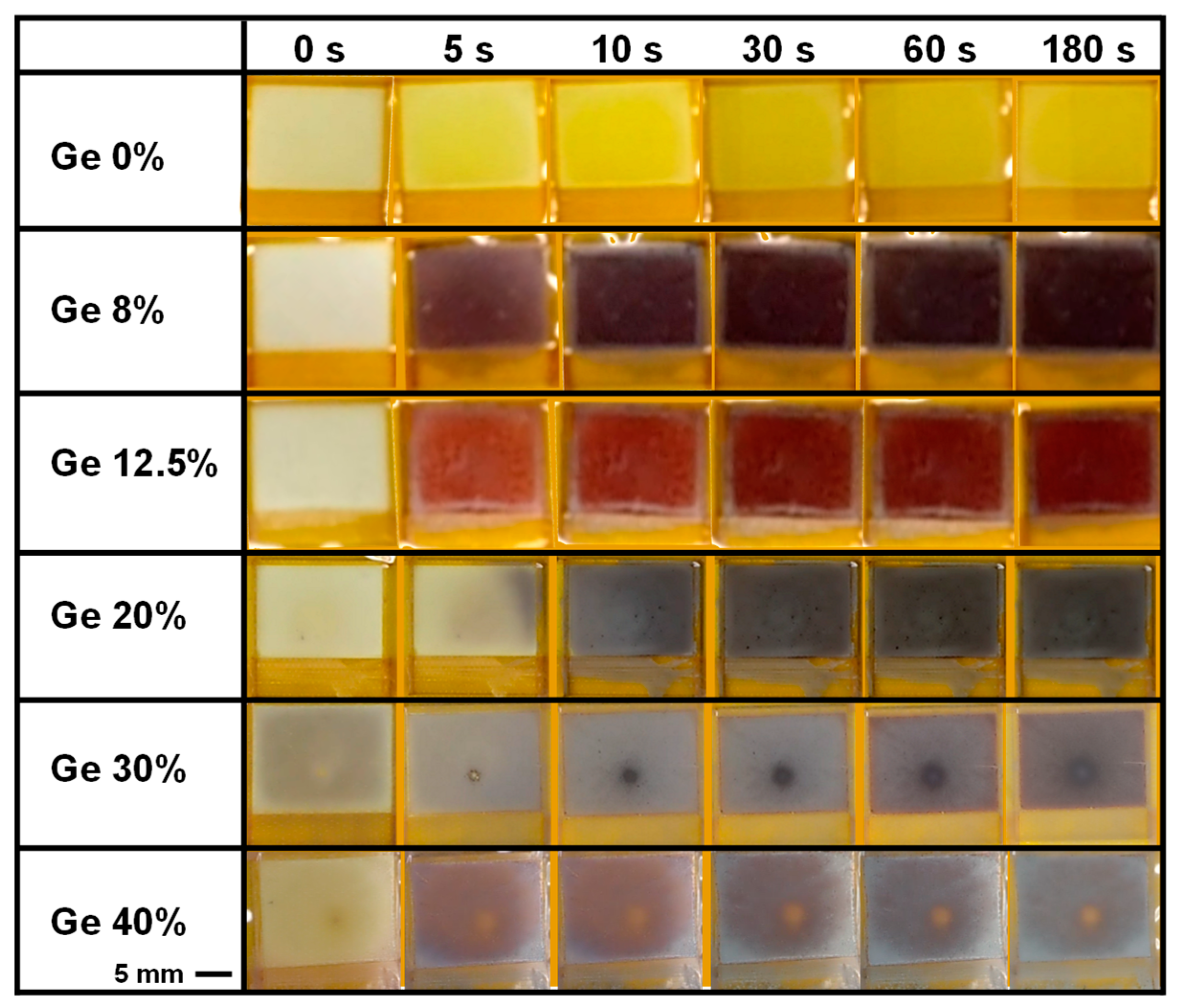
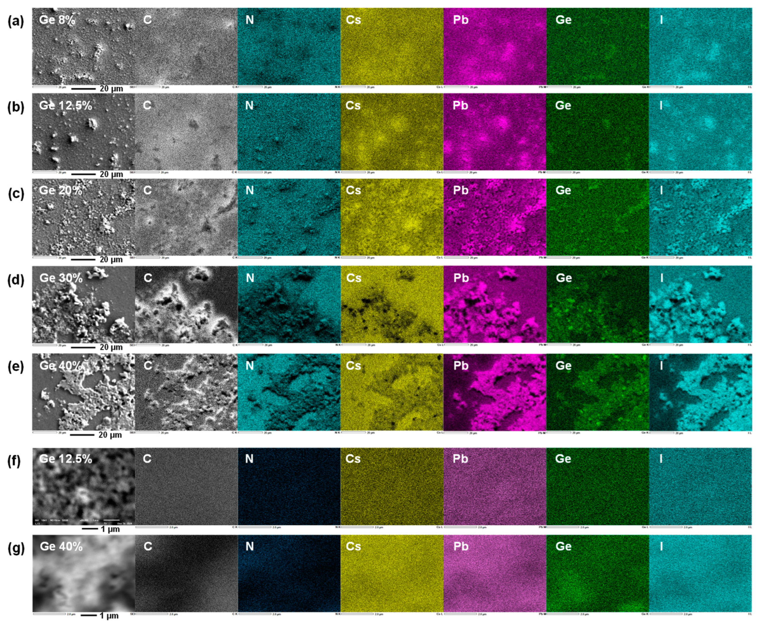
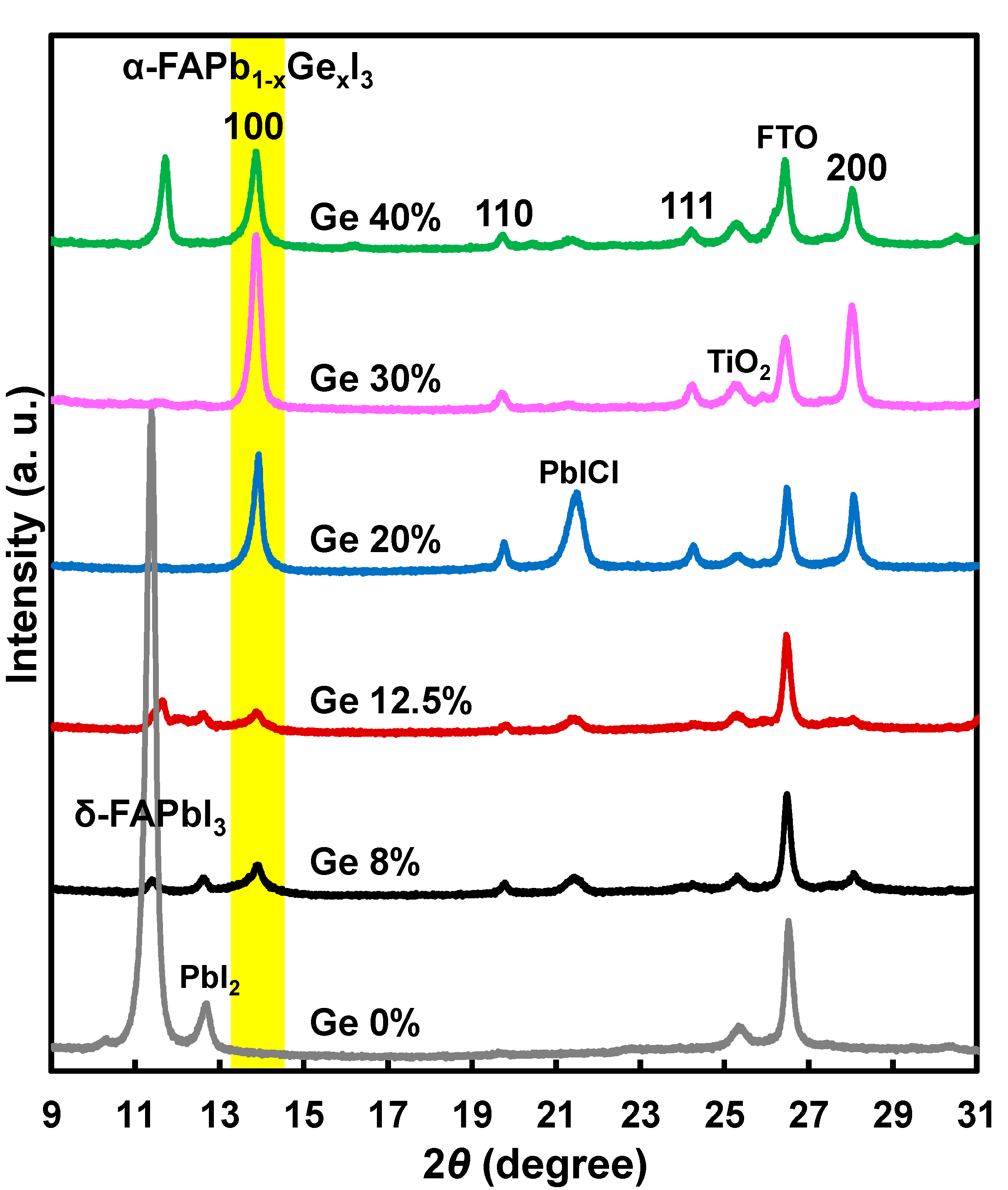
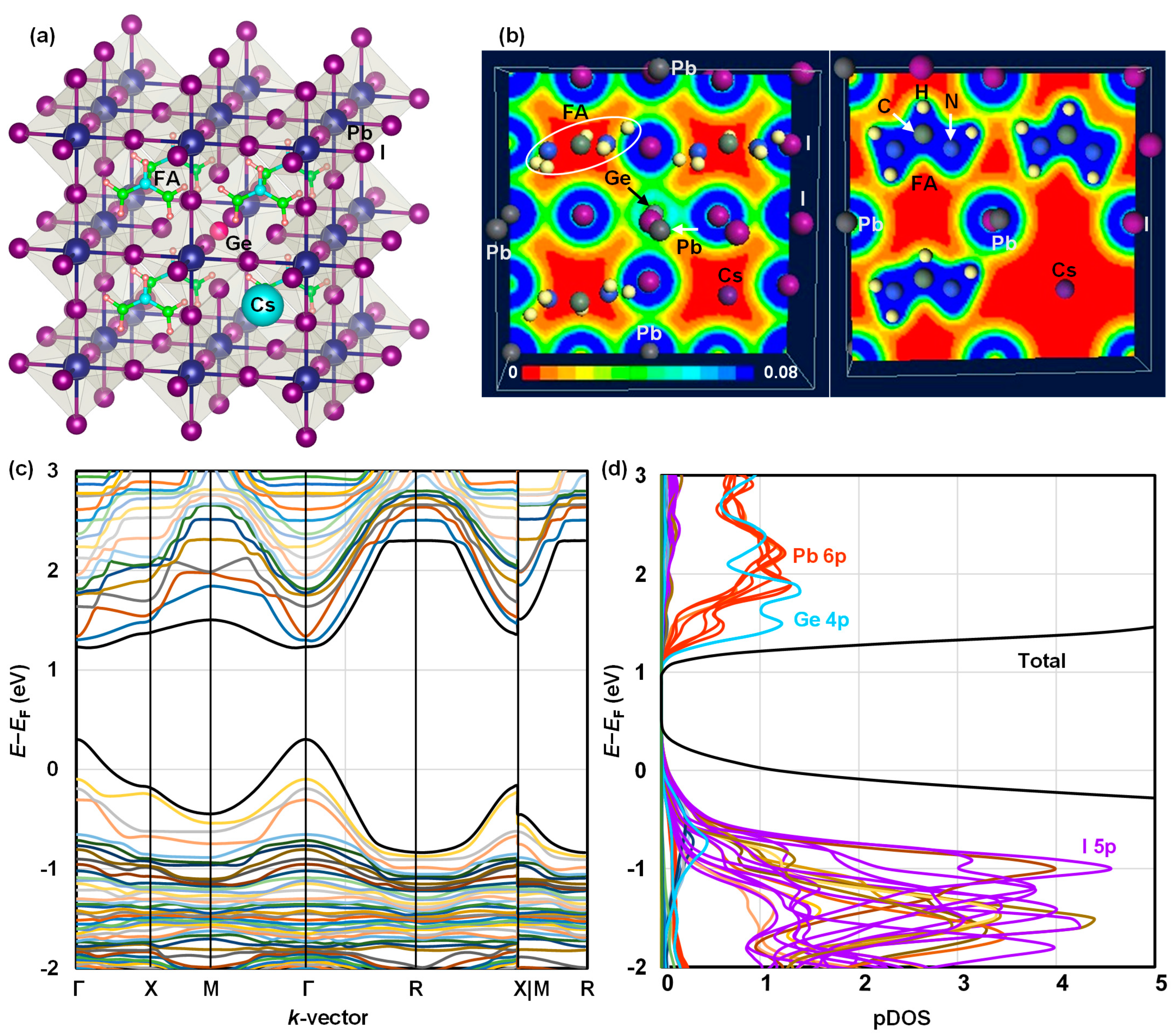
3. Results and Discussion
4. Conclusions
Author Contributions
Funding
Institutional Review Board Statement
Informed Consent Statement
Data Availability Statement
Acknowledgments
Conflicts of Interest
References
- Zhang, H.; Ji, X.; Yao, H.; Fan, Q.; Yu, B.; Li, J. Review on efficiency improvement effort of perovskite solar cell. Sol. Energy 2022, 233, 421–434. [Google Scholar] [CrossRef]
- Sharma, R.; Sharma, A.; Agarwal, S.; Dhaka, M.S. Stability and efficiency issues, solutions and advancements in perovskite solar cells: A review. Sol. Energy 2022, 244, 516–535. [Google Scholar] [CrossRef]
- Park, J.; Kim, J.; Yun, H.-S.; Paik, M.J.; Noh, E.; Mun, H.J.; Kim, M.G.; Shin, T.J.; Seok, S.I. Controlled growth of perovskite layers with volatile alkylammonium chlorides. Nature 2023, 616, 724–730. [Google Scholar] [CrossRef] [PubMed]
- Najarian, M.; Dinic, F.; Chen, H.; Sabatini, R.; Zheng, C.; Lough, A.; Maris, T.; Saidaminov, M.I.; García de Arquer, F.P.; Voznyy, O.; et al. Homomeric chains of intermolecular bonds scaffold octahedral germanium perovskites. Nature 2023, 620, 328–335. [Google Scholar] [CrossRef]
- Rao, M.K.; Sangeetha, D.N.; Selvakumar, M.; Sudhakar, Y.N.; Mahesha, M.G. Review on persistent challenges of perovskite solar cells’ stability. Sol. Energy 2021, 218, 469–491. [Google Scholar] [CrossRef]
- Magdalin, A.E.; Nixon, P.D.; Jayaseelan, E.; Sivakumar, M.; Devi, S.K.N.; Subathra, M.S.P.; Kumar, N.M.; Ananthi, N. Development of lead-free perovskite solar cells: Opportunities, challenges, and future technologies. Results Eng. 2023, 20, 101438. [Google Scholar] [CrossRef]
- Oku, T. Crystal structures of perovskite halide compounds used for solar cells. Rev. Adv. Mater. Sci. 2020, 59, 264–305. [Google Scholar] [CrossRef]
- Bu, T.; Li, J.; Li, H.; Tian, C.; Su, J.; Tong, G.; Ono, L.K.; Wang, C.; Lin, Z.; Chai, N.; et al. Lead halide–templated crystallization of methylamine-free perovskite for efficient photovoltaic modules. Science 2021, 372, 1327–1332. [Google Scholar] [CrossRef] [PubMed]
- Chen, S.; Pan, L.; Ye, T.; Lei, N.; Yang, Y.; Wang, X. The lattice reconstruction of Cs-introduced FAPbI1.80Br1.20 enables improved stability for perovskite solar cells. RSC Adv. 2021, 11, 3997–4005. [Google Scholar] [CrossRef] [PubMed]
- Khadka, D.B.; Shirai, Y.; Yanagida, M.; Tadano, T.; Miyano, K. Interfacial embedding for high-efficiency and stable methylammonium-free perovskite solar cells with fluoroarene hydrazine. Adv. Energy Mater. 2022, 12, 2202029. [Google Scholar] [CrossRef]
- Jeong, J.; Kim, M.; Seo, J.; Lu, H.; Ahlawat, P.; Mishra, A.; Yang, Y.; Hope, M.A.; Eickemeyer, F.T.; Kim, M.; et al. Pseudo-halide anion engineering for α-FAPbI3 perovskite solar cells. Nature 2021, 592, 381–385. [Google Scholar] [CrossRef] [PubMed]
- Chen, H.; Chen, Y.; Zhang, T.; Liu, X.; Wang, X.; Zhao, Y. Advances to high-performance black-phase FAPbI3 perovskite for efficient and stable photovoltaics. Small Struct. 2021, 2, 2000130. [Google Scholar] [CrossRef]
- Masi, S.; Gualdrón-Reyes, A.F.; Mora-Seró, I. Stabilization of Black Perovskite Phase in FAPbI3 and CsPbI3. ACS Energy Lett. 2020, 5, 1974–1985. [Google Scholar] [CrossRef]
- Li, R.; Song, J.; Peng, J.; Tian, X.; Xu, Y.; Huang, H.; Bai, S.; Li, Y.; Yao, F.; Lin, Q. Temperature-dependent performance metrics of tin-doped perovskite photodetectors. J. Mater. Chem. C 2022, 10, 1625–1631. [Google Scholar] [CrossRef]
- Enomoto, A.; Suzuki, A.; Oku, T.; Fukunishi, S.; Tachikawa, T.; Hasegawa, T. First-principles calculations and device characterizations of formamidiniumcesium lead triiodide perovskite crystals stabilized by germanium or copper. Jpn. J. Appl. Phys. 2023, 62, SK1015. [Google Scholar] [CrossRef]
- Kogo, A.; Yamamoto, K.; Murakami, T.N. Germanium ion doping of CsPbI3 to obtain inorganic perovskite solar cells with low temperature processing. Jpn. J. Appl. Phys. 2022, 61, 020904. [Google Scholar] [CrossRef]
- Yang, F.; Hirotani, D.; Kapil, G.; Kamarudin, M.A.; Ng, C.H.; Zhang, Y.; Shen, Q.; Hayase, S. All-inorganic CsPb1−xGexI2Br perovskite with enhanced phase stability and photovoltaic performance. Angew. Chem. Int. Ed. 2018, 57, 12745–12749. [Google Scholar] [CrossRef] [PubMed]
- Kim, G.M.; Ishii, A.; Öz, S.; Miyasaka, T. MACl-assisted Ge doping of Pb-hybrid perovskite: A universal route to stabilize high performance perovskite solar cells. Adv. Energy Mater. 2020, 10, 1903299. [Google Scholar] [CrossRef]
- Oku, T.; Ohishi, Y.; Ueoka, N. Highly (100)-oriented CH3NH3PbI3(Cl) perovskite solar cells prepared with NH4Cl using an air blow method. RSC Adv. 2018, 8, 10389–10395. [Google Scholar] [CrossRef]
- Zhang, W.; Li, Y.; Liu, X.; Tang, D.; Li, X.; Yuan, X. Ethyl acetate green antisolvent process for high-performance planar low-temperature SnO2-based perovskite solar cells made in ambient air. Chem. Eng. J. 2020, 379, 122298. [Google Scholar] [CrossRef]
- Liu, X.; Luo, D.; Lu, Z.-H.; Yun, J.S.; Saliba, M.; Seok, S.I.; Zhang, W. Stabilization of photoactive phases for perovskite photovoltaics. Nat. Rev. Chem. 2023, 7, 462–479. [Google Scholar] [CrossRef] [PubMed]
- Oku, T.; Taguchi, M.; Suzuki, A.; Kitagawa, K.; Asakawa, Y.; Yoshida, S.; Okita, M.; Minami, S.; Fukunishi, S.; Tachikawa, T. Effects of polysilane addition to chlorobenzene and high temperature annealing on CH3NH3PbI3 perovskite photovoltaic devices. Coatings 2021, 11, 665. [Google Scholar] [CrossRef]
- Ono, I.; Oku, T.; Genko, Y.; Okumura, R.; Nasu, T.; Mizuno, S.; Tachikawa, T.; Hasegawa, T.; Fukunishi, S. Stable decaphenylcyclopentasilane hole transport layers for double-stacked perovskite photovoltaic devices fabricated under ambient atmosphere. Chem. Inorg. Mater. 2024, 4, 100066. [Google Scholar] [CrossRef]
- Kuo, Y.-C.; Oku, T.; Suzuki, A.; Ono, I.; Okumura, R. Electronic structures of lead-free Sn- or Ge-hybrid perovskite halides studied by first-principles calculation. Hybrid Adv. 2024, 5, 100174. [Google Scholar] [CrossRef]
- Okumura, R.; Oku, T.; Suzuki, A. Accelerated formation of photoactive formamidinium-based lead triiodide perovskite crystals by the addition of copper iodide. Chem. Inorg. Mater. 2024, 3, 100052. [Google Scholar] [CrossRef]
- Zhang, T.; Chen, Y.; Kan, M.; Xu, S.; Miao, Y.; Wang, X.; Ren, M.; Chen, H.; Liu, X.; Zhao, Y. MA cation-induced diffusional growth of low-bandgap FA-Cs perovskites driven by natural gradient annealing. Research 2021, 2021, 9765106. [Google Scholar] [CrossRef] [PubMed]
- Yang, S.; Wu, M.; Lei, X.; Wang, J.; Han, Y.; He, X.; Liu, S.; Liu, Z. Ultra-high 1.27 V VOC of pure CsPbI3 perovskite solar cells with an efficiency of 21.8%. ACS Energy Lett. 2024, 9, 4817–4826. [Google Scholar] [CrossRef]

| Ge (%) | Solution Composition | FAI (mg) | PbI2 (mg) | GeI2 (mg) | MACl (mg) |
|---|---|---|---|---|---|
| 0 | FA0.95Cs0.05PbI3 | 81.7 | 230.5 | 0.0 | 13.5 |
| 8 | FA0.95Cs0.05Pb0.92Ge0.08I3 | 81.7 | 212.1 | 13.1 | 13.5 |
| 12.5 | FA0.95Cs0.05Pb0.875Ge0.125I3 | 81.7 | 201.7 | 20.4 | 13.5 |
| 20 | FA0.95Cs0.05Pb0.80Ge0.20I3 | 81.7 | 184.4 | 32.6 | 13.5 |
| 30 | FA0.95Cs0.05Pb0.7Ge0.30I3 | 81.7 | 161.4 | 49.0 | 13.5 |
| 40 | FA0.95Cs0.05Pb0.60Ge0.40I3 | 81.7 | 138.3 | 65.3 | 13.5 |
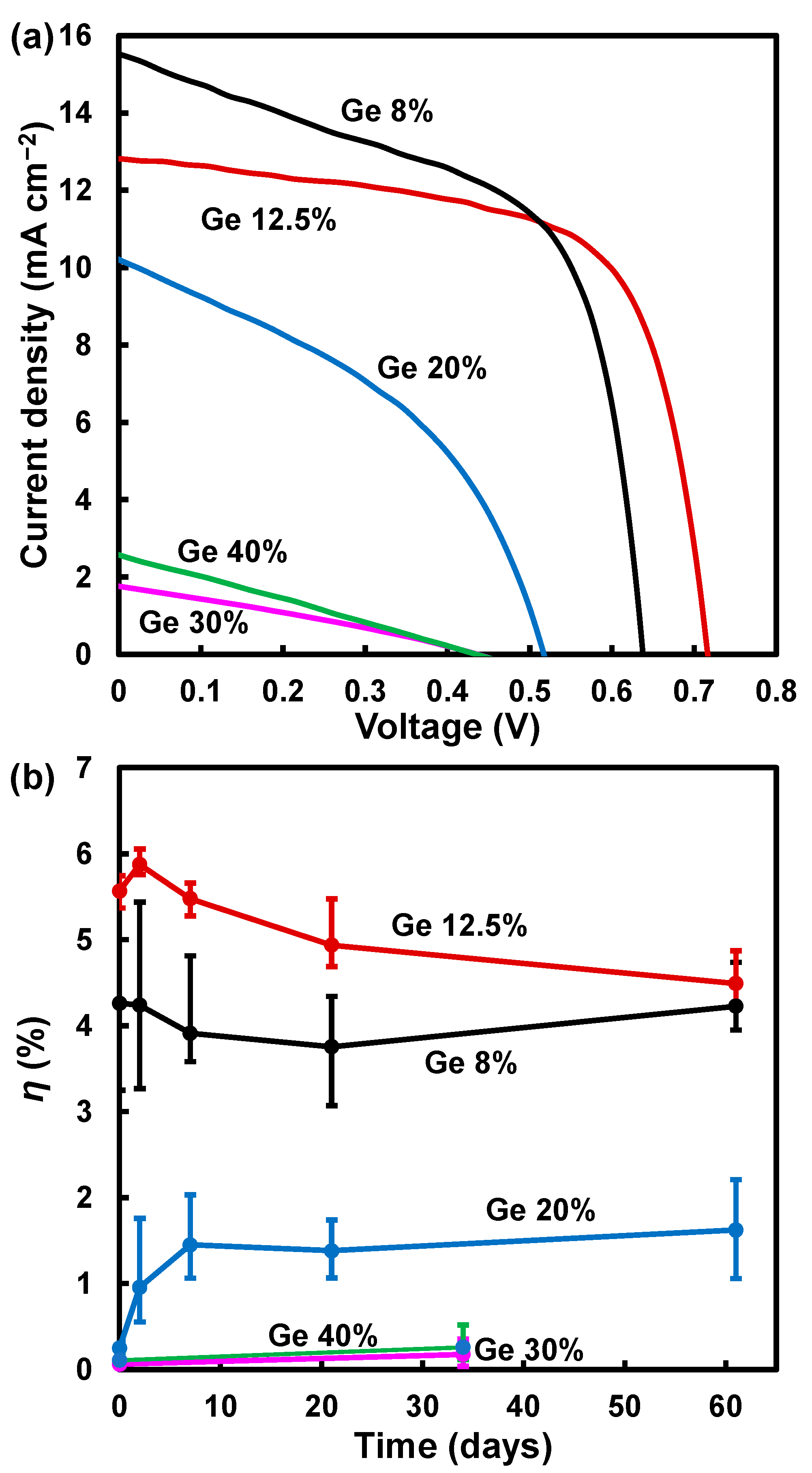
| Devices Ge (%) | JSC (mA cm−2) | VOC (V) | FF | η (%) | ηave (%) | a (Å) |
|---|---|---|---|---|---|---|
| 8 | 15.5 | 0.641 | 0.581 | 5.74 | 4.26 | 6.354(1) |
| 12.5 | 12.4 | 0.705 | 0.659 | 5.74 | 5.56 | 6.355(1) |
| 20 | 5.61 | 0.323 | 0.247 | 0.448 | 0.250 | 6.354(0) |
| 30 | 1.28 | 0.415 | 0.292 | 0.155 | 0.0923 | 6.362(8) |
| 40 | 1.78 | 0.451 | 0.258 | 0.207 | 0.0989 | 6.361(1) |
| After 2 days | ||||||
| 8 | 16.5 | 0.615 | 0.557 | 5.66 | 4.24 | - |
| 12.5 | 12.8 | 0.716 | 0.657 | 6.05 | 5.87 | - |
| 20 | 8.62 | 0.491 | 0.274 | 1.76 | 0.957 | - |
| After 7 days | ||||||
| 8 | 16.0 | 0.566 | 0.527 | 4.78 | 3.91 | - |
| 12.5 | 12.5 | 0.704 | 0.643 | 5.66 | 5.48 | - |
| 20 | 9.39 | 0.540 | 0.421 | 2.14 | 1.45 | - |
| After 21 days | ||||||
| 8 | 15.9 | 0.532 | 0.509 | 4.31 | 3.76 | |
| 12.5 | 12.6 | 0.694 | 0.627 | 5.48 | 4.93 | |
| 20 | 9.70 | 0.472 | 0.380 | 1.74 | 1.38 | |
| After 34 days | ||||||
| 30 | 2.83 | 0.545 | 0.311 | 0.479 | 0.303 | - |
| 40 | 3.93 | 0.460 | 0.232 | 0.420 | 0.166 | - |
| After 61 days | ||||||
| 8 | 15.4 | 0.573 | 0.535 | 4.72 | 4.23 | - |
| 12.5 | 11.6 | 0.684 | 0.616 | 4.87 | 4.49 | - |
| 20 | 10.2 | 0.516 | 0.418 | 2.20 | 1.62 | - |
Disclaimer/Publisher’s Note: The statements, opinions and data contained in all publications are solely those of the individual author(s) and contributor(s) and not of MDPI and/or the editor(s). MDPI and/or the editor(s) disclaim responsibility for any injury to people or property resulting from any ideas, methods, instructions or products referred to in the content. |
© 2025 by the authors. Licensee MDPI, Basel, Switzerland. This article is an open access article distributed under the terms and conditions of the Creative Commons Attribution (CC BY) license (https://creativecommons.org/licenses/by/4.0/).
Share and Cite
Enomoto, A.; Suzuki, A.; Oku, T.; Shimada, H. Promoted Formation of Photoactive α-Formamidinium Cesium Lead Triiodide Perovskite Crystals by Germanium Addition. Inorganics 2025, 13, 15. https://doi.org/10.3390/inorganics13010015
Enomoto A, Suzuki A, Oku T, Shimada H. Promoted Formation of Photoactive α-Formamidinium Cesium Lead Triiodide Perovskite Crystals by Germanium Addition. Inorganics. 2025; 13(1):15. https://doi.org/10.3390/inorganics13010015
Chicago/Turabian StyleEnomoto, Ayu, Atsushi Suzuki, Takeo Oku, and Haruto Shimada. 2025. "Promoted Formation of Photoactive α-Formamidinium Cesium Lead Triiodide Perovskite Crystals by Germanium Addition" Inorganics 13, no. 1: 15. https://doi.org/10.3390/inorganics13010015
APA StyleEnomoto, A., Suzuki, A., Oku, T., & Shimada, H. (2025). Promoted Formation of Photoactive α-Formamidinium Cesium Lead Triiodide Perovskite Crystals by Germanium Addition. Inorganics, 13(1), 15. https://doi.org/10.3390/inorganics13010015