Abstract
As devices become more miniaturized and integrated, the heat flux density has increased, highlighting the issue of heat concentration, especially for low thermal conductivity gallium oxide (Ga2O3). This study utilizes diamond composite substrates with an AlN transition layer to assist Ga2O3 in rapid thermal dissipation. All samples were prepared using pulsed laser deposition (PLD) and annealed at 600–1000 °C. The microstructure, surface morphology, vacancy defects, and thermal characteristics of post-annealed Ga2O3 were then thoroughly investigated to determine the mechanism by which annealing temperature influences the heat transfer of heterostructures. The results demonstrate that increasing the annealing temperature can improve the crystallinity of Ga2O3 while also reducing oxygen vacancy defects from 20.6% to 9.9%. As the temperature rises to 1000 °C, the thermal conductivity of Ga2O3 reaches a maximum of 12.25 W/(m·K). However, the interface microstructure has no direct correlation with annealing temperature. At 700 °C, Ga2O3/diamond exhibits a maximum thermal boundary conductance of 127.06 MW/(m2·K). Higher temperatures (>800 °C) cause irregular mixtures to form near the heterointerface, intensifying phonon interface scattering and sharply deteriorating interfacial heat transfer. These findings contribute to a better understanding of the heterointerface thermal transfer influence mechanism and provide theoretical guidance for the thermal management design and physical analysis of Ga2O3-based power devices.
1. Introduction
Electric vehicles (EVs) are rapidly expanding due to the consumers’ demand for energy conservation and emission reduction. Semiconductors, as the core of electronic products and the foundation of modern technology, may help to advance the development of EVs. Therefore, wide and ultra-wide bandgap semiconductor materials have received widespread attention. In contrast to the currently industrialized silicon carbide (SiC) and gallium nitride (GaN), emerging gallium oxide (Ga2O3) has an ultra-wide bandgap width (4.5–4.9 eV) and an ultra-high critical breakdown field (8 MV/cm), thus resulting in a higher voltage resistance and a lower power loss [1]. In addition, β-Ga2O3 prevails over other wide bandgap materials like SiC and GaN due to its low cost and scalable melting growth techniques, including edge-defined film-fed growth (EFG) and Czochralski methods [2,3]. Therefore, the growth rate of Ga2O3 single-crystal substrates is faster, the iteration cycle is shorter, and the manufacturing cost can be 78% less than SiC using iridium-free technology [4]. These characteristics have driven the development of β-Ga2O3-based power devices. In 2012, the National Institute of Information and Communications Technology (NICT) [5] demonstrated the first Ga2O3 metal-semiconductor field-effect transistors (MESFETs). Breakthroughs have continued to occur as research has progressed [5,6,7,8,9,10,11,12,13,14,15].
However, with the increasing power density, its extremely low natural thermal conductivity (10–27 W/m·K), only 1/30 of SiC and 1/10 of GaN [16], brings unavoidable issues of heat dissipation. Furthermore, Ga2O3 with thin films or nanowire structures can increase phonon-boundary scattering, further deteriorating its thermal conductivity [1,17,18]. Such low thermal conductance has become one of the technical bottlenecks in its application and promotion, and the resulting self-heating effect (SHE) can lead to an increase in the near-junction temperature of power devices and uneven distribution of dissipated power, resulting in the restricted stability, decreased device reliability, and shortened lifetime [19]. Thus, an effective thermal management strategy is urgently required. At present, a hetero-integration method has been proposed to minimize the SHE of β-Ga2O3 MOSFETs. This involves ion bonding or heterojunction growth of Ga2O3 with high thermal conductivity materials. The effectiveness of hetero-integration schemes in improving the high-temperature characteristics of Ga2O3 power devices has also been verified experimentally. In 2019, the Shanghai Institute of Microsystems [20] used an ion-cutting process to achieve hetero-integration of single-crystal Ga2O3 and SiC through bonding and prepared the high-temperature characteristics of switch devices. The electrical characterization results showed that SiC-based Ga2O3 devices had significantly higher thermal stability than Ga2O3-based Ga2O3 devices, including stable on-resistance, forward saturation current, and reverse leakage current being significantly advanced. In 2024, the same research group [21] achieved higher thermal conductivity of Ga2O3 and lower thermal boundary resistance (TBR) by introducing an Al2O3 intermediate layer and post-annealing to improve the quality of Ga2O3 films and the heterointerfaces. Although single-crystal Ga2O3 can be directly transferred to a high thermal conductivity substrate through mechanical exfoliation and ion bonding, this method has obvious limitations and is only suitable for research purposes, not for future industrial development. In contrast, heterogeneous growth with flexible process compatibility has a greater potential. When growing Ga2O3 directly on a high thermal conductivity substrate, it is important to consider the lattice mismatch between Ga2O3 and the high thermal conductivity substrate [4,22]. A larger lattice mismatch will generate a large number of defects and voids at the interface, further increasing thermal resistance and limiting interfacial heat transfer [4,22]. In addition, large differences in thermal expansion coefficients may generate large residual stress in the Ga2O3 layer, causing it to rupture during the heating and cooling process. These issues can be further addressed by using appropriate thermal interface materials (TIMs, proper lattice matching, thermal expansion coefficient, thickness, thermal conductivity, and crystal plane orientation) to reduce the thermal boundary resistance between the heterostructures [23,24,25].
The simulation results show that the higher the thermal conductivity of a substrate material as a heat sink, the greater the heat dissipation effect on the low thermal conductivity materials (such as GaN and Ga2O3) [26,27]. Diamond’s high thermal conductivity (1000–2000 W/(m·K)) makes it a popular choice for managing heat in low thermal conductivity materials and improving device performance [27]. In addition, transitions between different semiconductor materials are frequently carried out via intermediate layers to reduce various physical mismatches such as lattice mismatch, crystal type mismatch, interdiffusion, and antiphase domains between different semiconductor materials. Due to a large lattice mismatch of 11% between GaN and diamond, SiN and AlN are commonly used as interlayers, and a number of systematic studies have been conducted to investigate the thermal properties and influence mechanisms of GaN on diamonds with and without SiN and AlN interlayers [27]. It was found [28] that the introduction of the SiN intermediate layer can result in smooth interfaces without too much disorder, effectively reducing phonon scattering and obtaining an extremely low TBR of 6.5 m2·K/GW. Similarly, Jia et al. [29] further confirmed that forming a silicon–carbon–nitrogen (Si-C-N) layer between GaN and diamond results in a strong adhesion with a SiN interlayer and a lower TBR (<10 m2·K/GW). To reduce the impact of a significant mismatch of Ga2O3 with diamond, AlN was selected as the thermal interface material for Ga2O3/diamond. The published work mainly focuses on the optimization of the growth processes of Ga2O3 films on diamond composite substrates; however, the effect of these optimizations is limited [30].
The key to efficiently utilizing the high thermal conductivity of diamond is to optimize interface heat transfer and thus enhance overall heat dissipation performance. It is reported that thermal annealing technology has advanced significantly and has been widely used for material heat treatment. Such a post-treatment process can effectively improve the quality of the films and heterointerface by stress relaxation and recrystallization, thus further improving their thermal properties [21]. Zhe Cheng et al. [31] found that 800 °C annealing treatment can effectively remove the injection-induced strain in the film, and increase the thermal conductivity of β-Ga2O3 by more than twice. Michael et al. [32] obtained an enhanced thermal boundary conductance (TBC) of Ga2O3/4H-SiC from 66 MW/(m2·K) to 77 MW/(m2·K) after annealing at 800 °C for 1 h. Xu et al. [1] further employed a thinner 20 nm Al2O3 intermediate layer to form a Ga2O3/Al2O3/4H-SiC composite structure and then annealed at an even higher temperature of 900 °C, achieving a higher TBC of ~130 MW/m2·K. Recently, similar work has started to get on with Ga2O3/diamond. Seo et al. [33] adopted the mist chemical vapor deposition (CVD) method to prepare Ga2O3 on the diamond. They found that at a growth temperature of 500 °C, Ga2O3 becomes polycrystalline, and interface separation occurs. However, at higher temperatures (550 °C and 600 °C), only β phase Ga2O3 exists, and the interface adhesion remains stable after thermal treatment at 800 °C. These reports present an effective method to improve the heterointerface microstructure and thermal properties, but so far, few investigations involve the enhancement of Ga2O3/diamond interfacial thermal transport using thermal treatment, and the related influence mechanisms of heat transfer and regulation are yet to be fully figured out, so further research is required.
In the current work, diamond composite substrates consist of a ~180 nm thick AlN film and a ~300 um diamond bulk. AlN films were pre-grown using an RF magnetron sputtering system, and then Ga2O3 thin films were deposited using pulsed laser deposition (PLD). After deposition, post-annealing treatment was performed for comparative investigations to compare the effects of growth temperature on the microstructure, defect concentration, and thermal properties of Ga2O3 thin films on diamond composite substrates. By comprehensively exploring the element mixing, structural disorder, interface binding force, chemical bonding, crystal orientation, and roughness of heterointerfaces, the influence mechanism of annealing temperature on heat transfer at non-uniform interfaces is revealed.
2. Materials and Methods
2.1. Sample Preparations
The AlN film was prepared by radio frequency magnetron sputtering method at a growth pressure of 0.2 Pa and a growth temperature of 400 °C. After preparing the AlN films, they were vacuum encapsulated. Ga2O3 was then grown on the aforementioned diamond composite substrate using a Coherent COMPex 102 PLD system equipped with a KrF excimer laser source (wavelength of 248 nm, pulse width of 25 ns; Santa Clara, CA, USA). The Ga2O3 ceramic targets were made from high-purity Ga2O3 polycrystalline powder (99.999%, Alfa Aesar (China) Chemical Co., Ltd., Shanghai, China) by cold pressing andsintering in air at 1350 °C for 24 h [34]. The irradiation pulse laser frequency was 10 Hz, and the energy density was 1.0 J/cm2. The distance between the substrate and the Ga2O3 target was 50 mm. The growth pressure was 1 Pa, and the growth temperature was 650 °C. After 32,000 laser pulses, an appropriate amount of pure O2 was introduced to maintain the pressure at 200 Pa, and the temperature was lowered to 550 °C for in situ annealing for 30 min.
2.2. Characterizations
After the sample preparation was completed, multiple characterizations including X-ray diffraction (XRD), atomic force microscopy (AFM), X-ray photoelectron spectroscopy (XPS), high-resolution transmission electron microscopy (HRTEM), and time-domain thermal reflection (TDTR) were performed. A comprehensive study was conducted on the microstructure, chemical state, and thermal conductivity of Ga2O3, establishing the intrinsic relationship between post-annealing conditions and heterostructure quality. The formation and control mechanisms of defects were identified. Specifically, the crystallinity and crystal structure were evaluated using a Bruker D8 DISCOVER XRD spectrometer (Billerica, MA, USA) equipped with a 40 kV, 30 mA, and 1.54 Å Cu Ka radiation source. The surface morphology is characterized by the Brxuker Dimension ICON AFM system (Billerica, MA, USA) in tapping mode. Thermo FEI Talos F200S G2 TEM (Waltham, MA, USA), equipped with an energy-dispersive spectrometer (EDS), was used to extract cross-sectional information. The electronic structure was determined using Thermo ESALAB 250xi XPS (Waltham, MA, USA) with a monochromatic Al K α line as the radiation source (photon energy of 1486.6 eV). The standard C1s nuclear energy peak (binding energy of 284.80 eV) was used as the absolute binding energy scale. The AUTINST Pione-01 TDTR system (Shanghai, China) was used to collect thermal characteristics, which employs titanium: sapphire femtosecond lines as the laser source. The laser wavelength, pulse, energy, and frequency are 1064 nm, 80 fs, 25 nJ, and 80 MHz, respectively.
3. Results and Discussion
3.1. Surface and Interface Microstructure and Morphology Variation
XRD, AFM, and TEM were used to extract structural data, surface morphology, and sectional information to understand the effect of annealing temperature on the microstructure evolution behavior of Ga2O3 films, as well as the fundamental mechanism involved.
Figure 1a shows the XRD patterns of Ga2O3 thin films deposited and annealed on diamond composite substrates under different atmospheres at 900 °C. The Ga2O3 films annealed in Ar and N2 atmospheres at 900 °C were denoted as Ar-900 and N2-900, respectively. Several obvious diffraction peaks were detected. The peaks at 36.1°, 43.92°, 75.26°, and 76.25° belong to the peaks of AlN and diamond [31,35], while other peaks belong to the diffraction peaks of Ga2O3. The deposited Ga2O3 has poor crystallization behavior, whereas the annealed ones are polycrystalline. Annealed Ga2O3 samples have three diffraction peaks corresponding to the β phase: (−201), (−402), and (−603) [31]. It can be observed that after annealing in N2 and Ar atmospheres, the detected diffraction peaks of Ga2O3 have been enhanced. In addition, the peak enhancement is more pronounced and the FWHM is narrower in N2, which indicates that high-temperature annealing in N2 is more effective at improving the crystallinity of Ga2O3.
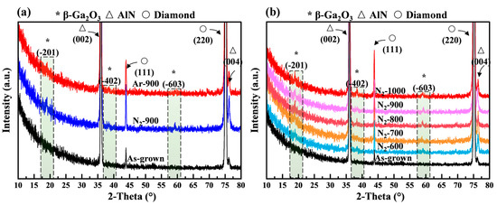
Figure 1.
XRD patterns of Ga2O3 on diamond composite substrates at different (a) ambients and (b) annealing temperatures.
Figure 1b shows the XRD patterns of Ga2O3 thin films on diamond composite substrates before and after annealing in an N2 ambient, indicating the structural evolution as a function of annealing temperature. The Ga2O3 films annealed in N2 atmosphere at 600 °C, 700 °C, 800 °C, 900 °C, and 1000 °C were denoted as N2-600, N2-700, N2-800, N2-900, and N2-1000, respectively. The β-Ga2O3 films are mostly (−201)-oriented, with peaks increasing with annealing temperature. Furthermore, it can be observed that as the annealing temperature increases, the FWHM slightly decreases, indicating that high temperature favors the improvement of film crystallinity. This is mainly because high-temperature annealing increases the kinetic energy of Ga and O atoms. Thus, the migration of atoms in the film can be accelerated to an appropriate level [36]. Meanwhile, the stress caused by lattice mismatch or distortion can be released, thereby promoting the preferred orientation of the crystal and improving the crystallinity of the films.
AFM micrographs were used to observe the surface morphology evolution of Ga2O3 films during high-temperature annealing, as shown in Figure 2 and Figure S1 (Supporting Information). The surface of deposited Ga2O3 is relatively rough (RMS of 7.43 nm) and contains small grains, mainly due to the high temperature providing sufficient energy for surface atoms to further migrate and condense, especially when annealed under N2, which shows a more noticeable increase than when annealed in Ar [36].
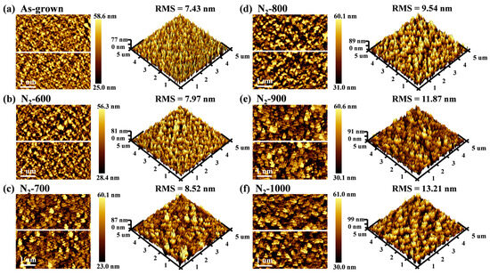
Figure 2.
AFM images of Ga2O3 films on diamond composite substrates at different annealing temperatures: (a) as-grown; (b) 600 °C; (c) 700 °C; (d) 800 °C; (e) 900 °C; (f) 1000 °C.
In addition, at elevated temperatures, evolved grain structures were observed in the 3D micrographs. The variation in surface morphology with annealing temperature is shown in Figure 2. As the annealing temperature increases, the phenomenon of grain aggregation becomes more pronounced, but overall three-dimensional growth dominates, and roughness increases steadily. At low annealing temperatures (600–700 °C), the increase in roughness is not minimal; however, when the temperature exceeds 800 °C, the roughness increases sharply. When the temperature reached 900 °C and 1000 °C, the roughness increased to 11.87 nm and 13.21 nm, respectively, showing an increase of 4.44 nm and 5.78 nm compared to the unannealed Ga2O3. The roughness rises with temperature. The increase in roughness with temperature may be due to local stress caused by crystallization within the film. Therefore, the increase in surface roughness at higher temperatures can be attributed to the combined effect of high temperatures and crystallization-induced stress in the nanocrystalline Ga2O3 film [37].
Figure 3 depicts the cross-sectional images and related electron diffraction patterns used to study microscopic changes in the interface quality of Ga2O3 heterostructures on diamond composite substrates with annealing temperature. Figure 3a shows the unannealed AlN/diamond interface. The presence of various crystal planes, and the deviation of the optical axis during the measurement, results in wrinkled stripes near the interface (within the rectangular box), which directly indicates that the crystal structure near the interface is relatively complex. In Figure 3b, the high-precision transmission electron microscopy (HRTEM) image of the Ga2O3/AlN heterostructure shows that the crystallinity of Ga2O3 is poor and presents polycrystalline, while AlN is similar to a single crystal. It was also found that there is a 3–5 nm disordered layer near the interface, and the signal superposition near the Ga2O3-AlN interface provides additional evidence. Figure 3c demonstrates that the horizontal lattice plane spacing in Ga2O3 is about 2.49 Å, which corresponds to the Ga2O3 (−402) plane [38].
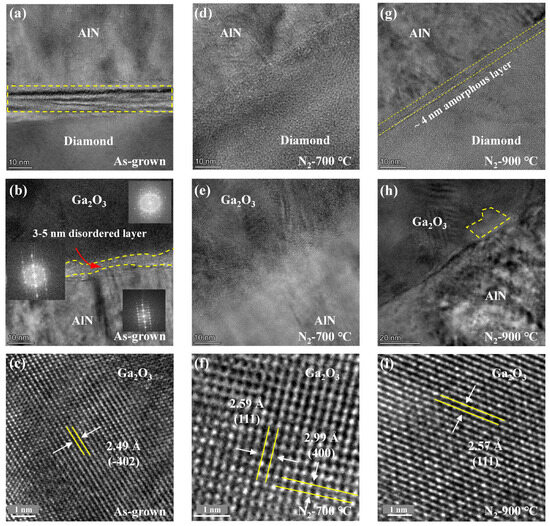
Figure 3.
HRTEM patterns of interface microstructure of Ga2O3 on diamond composite substrates at different annealing temperatures: (a–c) deposited state; (d–f) 700 °C; (g–i) 900 °C. Inserts in (b): FFT results of Ga2O3, Ga2O3/AlN, and AlN.
In a comparison of the HRTEM images of AlN and diamond interfaces after annealing, it can be found that wrinkled stripes disappear at 700 °C (Figure 3d). However, at 900 °C (Figure 3g), an amorphous layer with a thickness of ~4 nm is visible near the interface. By comparing the Ga2O3 and AlN interfaces after annealing, when the annealing temperature is 700 °C, the disordered layer near the interface almost disappears, as shown in Figure 3e. However, at 900 °C, abnormal areas appear near the interface, as shown in the yellow dashed line in Figure 3h. When comparing the interior of Ga2O3, as shown in Figure 3f,i, the measured interplanar spacing belongs to the β phase of Ga2O3, and the higher the annealing, the fewer types of diffraction fringes and the better the crystallinity. Herein, the interplanar spacings of 2.59 Å and 2.57 Å belong to the Ga2O3 (111) plane [39], while the interplanar spacing of 2.99 Å corresponds to the Ga2O3 (400) plane [40].
Figure 4 shows a detailed analysis of the abnormal changes near the Ga2O3-AlN interface at 900 °C in Figure 3h. Figure 4a–c show that the Ga2O3 heterointerface on the diamond composite substrate under HAADF mode has a significant interface mutation at unannealed and 700 °C. However, at 900 °C, it is evident that there are some unknown structures densely arranged near the interface that extend into the interior of Ga2O3. For further analysis, this section focuses on one of the small areas as shown in Figure 4d. The elemental composition of the thin film cross-section was determined using the EDS technique. Figure 4e depicts the mapping images of O, Ga, Al, and N elements, which qualitatively shows the constituent elements. Figure 4e provides further quantitative analysis of the abnormal region: the yellow region contains 11.50%, 41.00%, 23.45%, and 24.05% of Ga, O, Al, and N atoms, respectively. It can be seen that in the abnormal area, some AlN penetrates the interior of Ga2O3 and forms a mixture with it.
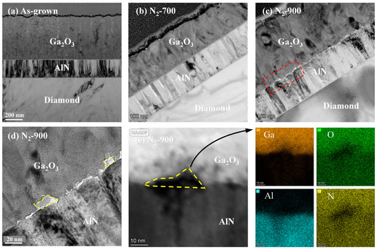
Figure 4.
TEM images of interface microstructure of Ga2O3 on diamond composite substrates at different annealing temperatures: (a) as-grown; (b) 700 °C; (c–e) 900 °C. (e) Distribution of Ga, O, Al, and N elements within the yellow dashed line.
3.2. Surface Vacancy Defects Analysis
The chemical composition and elemental state of Ga2O3 thin films before and after annealing were determined using XPS. To eliminate the charge effect, the C1s peak at 284.80 eV was used to calibrate the binding energy [35,41,42]. Figure 5a–c show the surface chemical composition of Ga2O3 before and after annealing, as well as the fine spectra of O 1s and Ga 3d. It can be seen that the elements detected on the surface are mainly composed of Ga, O, and C.
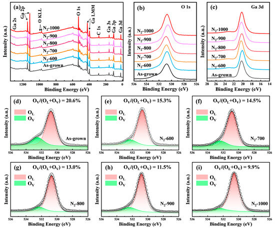
Figure 5.
(a) XPS survey, (b) O 1s, and (c) Ga 3d of Ga2O3 films on diamond composite substrates at different annealing temperatures. (d–i) O 1s peak fitting.
Figure 5d–i show that the O 1s core level of all samples was deconvoluted into OL (centered at 530.8 eV) and OV (centered at 532.1 eV), with the former corresponding to Ga-O bonds, and the latter related to oxygen vacancies [43]. Comparing the oxygen vacancy defects’ dependence on the annealing ambients, Figure S2 (Supporting Information) shows that the proportion of OV defects significantly decreased after annealing, with the lowest concentration of vacancy defects obtained by annealing in the N2 ambient. This is mainly due to N atoms occupying some oxygen vacancy defects. Further, Figure 5d–i also show the proportion of oxygen vacancy (OV/(OL + OV)), which decreases as the N2 annealing temperature increases. This can be partially explained by the fact that N atoms occupy some oxygen vacancies at a high temperature by forming Ga-N bonds, as verified by the slight shift of Ga 3d spectra toward a low-energy direction, and thus reduce the proportion of oxygen vacancies [44]. However, in such a severely oxygen-deficient atmosphere, the huge reduction from 20.6% to 9.9% is not reasonable. A non-pure N2 annealing atmosphere can be responsible for the results. Before annealing, the air inside the furnace tube might be not completely expelled, resulting in an air and N2 mixture annealing atmosphere. A high temperature allows oxygen atoms to obtain sufficient energy to participate in the formation of Ga2O3 [42]. As the temperature increases, the remaining oxygen atoms are nearly exhausted, and then a slight reduction of VO is contributed by a small amount of N atoms doped into Ga2O3. This work has not continuously tracked the root cause of this result. In the future, comparative experiments will be designed and will strictly control the mixing ratio of air and N2 to reveal the physical influence mechanism.
3.3. Thermal Properties Measurements
After preliminary analysis of the microstructure and defects after annealing in different environments, it was discovered that the quality of Ga2O3 after N2 annealing is improved. Time-domain thermal reflectance (TDTR) measurements were conducted to investigate the thermal conductivity characteristics of Ga2O3 heterostructures on diamond composite substrates before and after annealing. TDTR is a high-precision and high temporal resolution measurement technique, widely used to study the thermal properties of various materials, including the thermal conductivity (κ) and heat capacity of single-layer and multi-layer films, and liquid materials, as well as the thermal boundary conductance (TBC) at solid–solid, solid–liquid, and microstructural interfaces [45]. In this study, the AUTINST Pioneer-01 time-domain thermal reflectance (TDTR) system was employed to quantify the κ of Ga2O3, as well as the TBC of Ga2O3/AlN and AlN/diamond interfaces. A schematic representation of a typical TDTR setup is depicted in Figure 6. Specifically, the sample is rapidly heated by irradiating its surface with a stronger laser pulse (pump pulse). Subsequently, weaker pulses (probe pulses) are applied to the same location at varying time delays, and the intensity of the reflected probe pulses is measured. By analyzing both the amplitude and phase shift of these reflected pulses, the temperature decay is tracked, thus determining the material’s reflectivity changes. Through further analysis of the reflectance variation and fitting the data to a thermal model, key parameters such as thermal conductivity, specific heat capacity, and TBC are extracted. Additionally, by minimizing the discrepancy between the TDTR signal and a heat transfer model, the required thermal performance metrics can be accurately estimated [46,47].
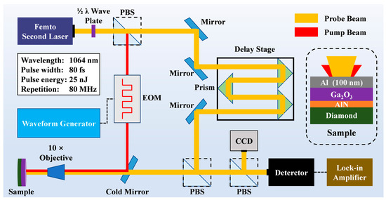
Figure 6.
Schematic of the typical TDTR setup. The acronyms EOM and PBS stand for electro-optic modulator and polarizing beam splitter, respectively.
Before measuring, aluminum films were first deposited onto the surface of samples to act as a transducer layer. The data fitting starts from the liner region, and to accurately fit, the relevant thermophysical parameters were taken from the literature [48,49,50]. Figure S3 (Supporting Information) gives the TDTR experimental data for each sample. The thermal conductivity of Ga2O3 (κGaO) and thermal boundary conductance of Ga2O3/diamond (TBCGaO-dia) without annealing were determined through numerical fitting to be 7.80 W/(m·K) and 31.34 MW/(m2·K), respectively. In contrast, after annealing in N2, the values were 11.09 W/(m·K) and 62.69 MW/(m2·K), respectively. After annealing in Ar, the values were 9.04 W/(m·K) and 59.43 MW/(m2·K), respectively. The thermal conductivity change of Ga2O3 corresponds to changes in crystallinity and defect concentration. Annealing at high temperatures in N2 improves both κGaO and TBCGaO-dia.
Characterizing and analyzing the physical and chemical properties of Ga2O3 on diamond composite substrates under the influence of N2 annealing temperature leads to the conclusion that the higher the annealing temperature, the better the quality of Ga2O3. On the one hand, the introduction of vacancies results in a mass disorder relative to β-Ga2O3 with the perfect unit cell, due to the missing O atom at the vacancy site. This contributes to a change in the effective reduced mass [51], while atomic-level defects result in the scattering of phonons due to differences in mass or the generation of strain fields. The scattering cross-sections follow Rayleigh scattering in different phonon modes. Furthermore, the existence of vacancy sites has been observed to increase phonon scattering, suppress the intensity of vibrational modes, and reduce the phonon mean free paths, which ultimately leads to a reduction in thermal conductivity.
On the other hand, vacancy defects can intensify the scattering effect between phonons and defects, expand the phonon dispersion curve of the material (Figure 7), and abbreviate the phonon relaxation time while impeding the participation rate of phonon vibration modes, thereby reducing the thermal conductivity [51].
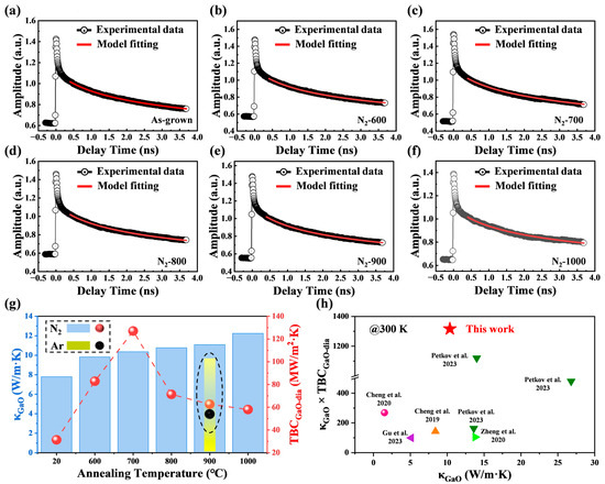
Figure 7.
TDTR signal intensity versus delay time at different annealing temperatures: (a) as-grown; (b) 600 °C; (c) 700 °C; (d) 800 °C; (e) 900 °C; (f) 1000 °C. (g) The variation in thermal characteristics parameters of Ga2O3 on diamond composite substrates versus annealing temperature. (h) Summary of κGaO versus (κGaO × TBCGaO-dia) reported in the literature [16,35,52,53,54].
However, the changes near the heterostructure interface are not linearly related to the annealing temperature. To investigate the effect of annealing on the thermal conductivity of heterostructures, Figure 7a–f show the TDTR measurement data along with fitting curves. Figure 7g shows the thermal conductivity of Ga2O3 on diamond composite substrates and the variation in Ga2O3 diamond interface thermal conductivity as functions of annealing temperature. The thermal conductivity (κGaO) of Ga2O3 monotonically increases with annealing temperature, indicating a positive correlation between the quality of Ga2O3 and the annealing temperature. However, as the annealing temperature increases, the interfacial thermal conductance reaches a critical point. Specifically, when the temperature increases from room temperature to 700 °C, the TBCGaO-dia increases until it reaches its maximum value. However, when the temperature exceeds 800 °C, TBCGaO-dia begins to decrease monotonically, indicating that the higher the temperature, the harder the interfacial thermal transfer. According to the above interface microstructure analysis, at lower temperatures, the microstructure near the interface undergoes a positive transformation, with the interface atoms gradually becoming more ordered. However, at high annealing temperatures, negative changes occur near the interface, such as the formation of an amorphous layer and irregular mixture, which results in enhanced phonon boundary scattering and thus hinders interface heat transfer. The high temperature helps to improve the thermal characteristics of heterostructures, but an excessive temperature can have adverse effects on heterostructures. In this study, the optimal process parameter for high thermal conductivity and interface heat conduction is 700 °C. Furthermore, to facilitate comparison, we defined (κGaO × TBCGaO-dia) as a dimensionless parameter. Figure 7h shows that, when compared to the literature [16,35,52,53,54], this study has the highest value for this parameter at 300 K.
4. Conclusions
This study investigates how annealing temperature influences the thermal properties of Ga2O3 thin films on diamond composite substrates. As the temperature increases, the crystallinity of Ga2O3 thin films on diamond composite substrates improves, and more N atoms are incorporated, effectively suppressing oxygen vacancy defects. The quality of Ga2O3 films is positively correlated with annealing temperature, reaching a maximum value of 12.25 W/(m·K) at 1000 °C. The thermal boundary conductance of Ga2O3/diamond heterojunction fluctuates greatly under the influence of high temperatures, with TBCGaO-dia showing significant enhancement in the range of 600–700 °C. However, at high temperatures (>800 °C), the interfacial thermal transport between Ga2O3 and diamond is hindered by the amorphous layers and the irregular mixtures, resulting in a decreasing trend in TBCGaO-dia. In summary, a compromise was achieved at 700 °C with a relatively high κGaO of 10.36 W/(m·K) and a maximum TBCGaO-dia of 127.06 MW/(m2·K), making it an optimal process parameter. These findings represent a promising method to enhance interfacial thermal transport across Ga2O3-diamond, deepen our understanding of how interface microstructure influences interfacial heat transfer, and provide guidance for designing and optimizing thermal management of Ga2O3 and other materials.
Supplementary Materials
The following supporting information can be downloaded at: https://www.mdpi.com/article/10.3390/c10030080/s1, Figure S1: AFM images of Ga2O3 films on diamond composite substrates at different annealing atmospheres: (a) as-grown; (b) Ar; (c) N2. Figure S2: (a) XPS survey, (b) O 1s, and (c) Ga 3d of Ga2O3 films on diamond composite substrates at different annealing atmospheres. (d–i) O 1s peak fitting. Figure S3. TDTR signal intensity versus delay time at different annealing atmospheres: (a) as-grown; (b) N2; (c) Ar.
Author Contributions
Conceptualization, H.M. and Q.Z.; methodology, H.M., Q.Z. and L.G.; software, Y.Z.; formal analysis, L.G.; investigation, Y.S. and W.C.; resources, Q.Z.; writing—original draft, L.G.; writing—review and editing, H.M. and Q.Z.; visualization, L.G.; supervision, H.M.; project administration, H.M. and Q.Z.; funding acquisition, H.M. and Q.Z. All authors have read and agreed to the published version of the manuscript.
Funding
This research was funded by the Science and Technology Innovation Plan of Shanghai Science and Technology Commission (No. 21DZ1100800, 23ZR1405300, 20501110700, and 20501110702).
Data Availability Statement
The raw/processed data required to reproduce these findings cannot be shared at this time as the data also forms part of an ongoing study.
Conflicts of Interest
The authors declare no conflicts of interest.
References
- Xu, W.; You, T.; Wang, Y.; Shen, Z.; Liu, K.; Zhang, L.; Sun, H.; Qian, R.; An, Z.; Mu, F.; et al. Efficient thermal dissipation in wafer-scale heterogeneous integration of single-crystalline β-Ga2O3 thin film on SiC. Fundam. Res. 2021, 1, 691–696. [Google Scholar] [CrossRef]
- Mu, W.; Jia, Z.; Yin, Y.; Hu, Q.; Li, Y.; Wu, B.; Zhang, J.; Tao, X. High quality crystal growth and anisotropic physical characterization of β-Ga2O3 single crystals grown by EFG method. J. Alloys Compd. 2017, 714, 453–458. [Google Scholar] [CrossRef]
- Galazka, Z.; Fiedler, A.; Popp, A.; Ganschow, S.; Kwasniewski, A.; Seyidov, P.; Pietsch, M.; Dittmar, A.; Anooz, S.B.; Irmscher, K.; et al. Bulk single crystals and physical properties of β-(AlxGa1−x)2O3 (x = 0–0.35) grown by the Czochralski method. J. Appl. Phys. 2023, 133, 035702. [Google Scholar] [CrossRef]
- Yan, Y.; Jin, Z.; Zhang, H.; Yang, D. Recent progresses in thermal treatment of β-Ga2O3 single crystals and devices. Int. J. Miner. 2024, 31, 1659–1677. [Google Scholar] [CrossRef]
- Higashiwaki, M.; Sasaki, K.; Kuramata, A.; Masui, T.; Yamakoshi, S. Gallium oxide (Ga2O3) metal-semiconductor field-effect transistors on single-crystal β-Ga2O3 (010) substrates. Appl. Phys. Lett. 2012, 100, 013504. [Google Scholar] [CrossRef]
- Zeng, K.; Vaidya, A.; Singisetti, U. 1.85 kV Breakdown Voltage in Lateral Field-Plated Ga2O3 MOSFETs. IEEE Electron Device Lett. 2018, 39, 1385–1388. [Google Scholar] [CrossRef]
- Green, A.J.; Chabak, K.D.; Heller, E.R.; Fitch, R.C.; Baldini, M.; Fiedler, A.; Irmscher, K.; Wagner, G.; Galazka, Z.; Tetlak, S.E.; et al. 3.8-MV/cm Breakdown Strength of MOVPE-Grown Sn-Doped Ga2O3 MOSFETs. IEEE Electron Device Lett. 2016, 37, 902–905. [Google Scholar] [CrossRef]
- Wang, C.; Gong, H.; Lei, W.; Cai, Y.; Hu, Z.; Xu, S.; Liu, Z.; Feng, Q.; Zhou, H.; Ye, J.; et al. Demonstration of the p-NiOx/n-Ga2O3 Heterojunction Gate FETs and Diodes With BV2/Ron,sp Figures of Merit of 0.39 GW/cm2 and 1.38 GW/cm2. IEEE Electron Device Lett. 2021, 42, 485–488. [Google Scholar] [CrossRef]
- Higashiwaki, M.; Sasaki, K.; Wong, M.H.; Kamimura, T.; Krishnamurthy, D.; Kuramata, A.; Masuio, T.; Yamakoshi, S. Depletion-mode Ga2O3 metal-oxide-semiconductor field-effect transistors on β-Ga2O3 (010) substrates and temperature dependence of their device characteristics. Appl. Phys. Lett. 2013, 103, 123511. [Google Scholar] [CrossRef]
- Lv, Y.; Zhou, X.; Long, S.; Wang, Y.; Song, X.; Zhou, X.; Xu, G.; Liang, S.; Feng, Z.; Cai, S.; et al. Enhancement-Mode β-Ga2O3 Metal-Oxide-Semiconductor Field-Effect Transistor with High Breakdown Voltage over 3000 V Realized by Oxygen Annealing. Phys. Status Solidi-R 2019, 14, 1900586. [Google Scholar] [CrossRef]
- Wong, M.H.; Sasaki, K.; Kuramata, A.; Yamakoshi, S.; Higashiwaki, M. Field-Plated Ga2O3 MOSFETs With a Breakdown Voltage of Over 750 V. IEEE Electron Device Lett. 2016, 37, 212–215. [Google Scholar] [CrossRef]
- Sharma, S.; Zeng, K.; Saha, S.; Singisetti, U. Field-Plated Lateral Ga2O3 MOSFETs With Polymer Passivation and 8.03 kV Breakdown Voltage. IEEE Electron Device Lett. 2020, 41, 836–839. [Google Scholar] [CrossRef]
- Hwang, W.S.; Verma, A.; Peelaers, H.; Protasenko, V.; Rouvimov, S.; Xing, H.; Seabaugh, A.; Haensch, W.; de Walle, C.V.; Galazka, Z.; et al. High-voltage field effect transistors with wide-bandgap β-Ga2O3 nanomembranes. Appl. Phys. Lett. 2014, 104, 203111. [Google Scholar] [CrossRef]
- Wang, C.; Zhou, H.; Zhang, J.; Mu, W.; Wei, J.; Jia, Z.; Zheng, X.; Luo, X.; Tao, X.; Hao, Y. Hysteresis-free and μs-switching of D/E-modes Ga2O3 hetero-junction FETs with the BV2/Ron,sp of 0.74/0.28 GW/cm2. Appl. Phys. Lett. 2022, 120, 112101. [Google Scholar] [CrossRef]
- Chabak, K.D.; McCandless, J.P.; Moser, N.A.; Green, A.J.; Mahalingam, K.; Crespo, A.; Hendricks, N.; Howe, B.M.; Tetlak, S.E.; Leedy, K.; et al. Recessed-Gate Enhancement-Mode β-Ga2O3 MOSFETs. IEEE Electron Device Lett. 2018, 39, 67–70. [Google Scholar] [CrossRef]
- Cheng, Z.; Wheeler, V.D.; Bai, T.; Shi, J.; Tadjer, M.J.; Feygelson, T.; Hobart, K.D.; Goorsky, M.S.; Graham, S. Integration of polycrystalline Ga2O3 on diamond for thermal management. Appl. Phys. Lett. 2020, 116, 062105. [Google Scholar] [CrossRef]
- Szwejkowski, C.J.; Creange, N.C.; Sun, K.; Giri, A.; Donovan, B.F.; Constantin, C.; Hopkins, P.E. Size effects in the thermal conductivity of gallium oxide (β-Ga2O3) films grown via open-atmosphere annealing of gallium nitride. J. Appl. Phys. 2015, 117, 084308. [Google Scholar] [CrossRef]
- Zhang, Y.; Su, Q.; Zhu, J.; Koirala, S.; Koester, S.J.; Wang, X. Thickness-dependent thermal conductivity of mechanically exfoliated β-Ga2O3 thin films. Appl. Phys. Lett. 2020, 116, 202101. [Google Scholar] [CrossRef]
- Zhou, X.; Xu, G.; Long, S. A large-area multi-finger β-Ga2O3 MOSFET and its self-heating effect. J. Semicond. 2023, 44, 072804. [Google Scholar] [CrossRef]
- Xu, W.; Zhang, Y.; Hao, Y.; Wang, X.; Wang, Y.; You, T.; Ou, X.; Han, G.; Hu, H.; Zhang, S.; et al. First Demonstration of Waferscale Heterogeneous Integration of Ga2O3 MOSFETs on SiC and Si Substrates by Ion-Cutting Process. In Proceedings of the 2019 International Electron Devices Meeting (IEDM), San Francisco, CA, USA, 7–11 December 2019; pp. 12.15.11–12.15.14. [Google Scholar]
- Xu, W.; Zhao, T.; Zhang, L.; Liu, K.; Sun, H.; Qu, Z.; You, T.; Yi, A.; Huang, K.; Han, G.; et al. Thermal Transport Properties of β-Ga2O3 Thin Films on Si and SiC Substrates Fabricated by an Ion-Cutting Process. ACS Appl. Electron. Mater. 2024, 6, 1710–1717. [Google Scholar]
- Sun, Z.; Zhang, D.; Qi, Z.; Wang, Q.; Sun, X.; Liang, K.; Dong, F.; Zhao, Y.; Zou, D.; Li, L.; et al. Insight into Interfacial Heat Transfer of β-Ga2O3/Diamond Heterostructures via the Machine Learning Potential. ACS Appl. Mater. Inter. 2024, 16, 31666–31676. [Google Scholar] [CrossRef] [PubMed]
- Jia, X.; Huang, L.; Sun, M.; Zhao, X.; Wei, J.; Li, C. The Effect of Interlayer Microstructure on the Thermal Boundary Resistance of GaN-on-Diamond Substrate. Coatings 2022, 12, 672. [Google Scholar] [CrossRef]
- Noh, J.; Chowdhury, P.R.; Segovia, M.; Alajlouni, S.; Si, M.; Charnas, A.R.; Huang, S.; Maize, K.; Shakouri, A.; Xu, X.; et al. Enhancement of Thermal Transfer From β-Ga2O3 Nano-Membrane Field-Effect Transistors to High Thermal Conductivity Substrate by Inserting an Interlayer. IEEE Trans. Electron Devices 2022, 69, 1186–1190. [Google Scholar] [CrossRef]
- Cheng, Z.; Mu, F.; Yates, L.; Suga, T.; Graham, S. Interfacial Thermal Conductance across Room-Temperature-Bonded GaN/Diamond Interfaces for GaN-on-Diamond Devices. ACS Appl. Mater. Inter. 2020, 12, 8376–8384. [Google Scholar] [CrossRef]
- Liu, C.; He, H.; Zhou, X.; Liu, W. Influence of Substrate and Gate Insulator on the Thermal Characteristics of β-Ga2O3 Field-Effect Transistors: A Simulation Study. Electronics 2022, 11, 2323. [Google Scholar] [CrossRef]
- Tijent, F.Z.; Faqir, M.; Chouiyakh, H.; Essadiqi, E.H. Review-Integration Methods of GaN and Diamond for Thermal Management Optimization. ECS J. Solid State Sci. Technol. 2021, 10, 74003. [Google Scholar] [CrossRef]
- Zhou, Y.; Anaya, J.; Pomeroy, J.; Sun, H.; Gu, X.; Xie, A.; Beam, E.; Becker, M.; Grotjohn, T.A.; Lee, C.; et al. Barrier-Layer Optimization for Enhanced GaN-on-Diamond Device Cooling. ACS Appl. Mater. Inter. 2017, 9, 34416–34422. [Google Scholar] [CrossRef] [PubMed]
- Gu, Y.; Zhang, Y.; Hua, B.; Ni, X.; Fan, Q.; Gu, X. Interface Engineering Enabling Next Generation GaN-on-Diamond Power Devices. J. Electron. Mater. 2021, 50, 4239–4249. [Google Scholar] [CrossRef]
- Gu, L.; Ma, H.-P.; Shen, Y.; Zuo, Y.; Tang, Z.; Zhang, Q.-C. Optimization of Heteroepitaxial Gallium Oxide Thin Films on Diamond Composite Substrates using Pulsed Laser Deposition Method. In Proceedings of the 2023 20th China International Forum on Solid State Lighting & 2023 9th International Forum on Wide Bandgap Semiconductors (SSLCHINA: IFWS), Xiamen, China, 27–30 November 2023; pp. 296–299. [Google Scholar]
- Cheng, Z.; Mu, F.; You, T.; Xu, W.; Shi, J.; Liao, M.E.; Wang, Y.; Huynh, K.; Suga, T.; Goorsky, M.S.; et al. Thermal Transport across Ion-Cut Monocrystalline β-Ga2O3 Thin Films and Bonded β-Ga2O3-SiC Interfaces. ACS Appl. Mater. Interfaces 2020, 12, 44943–44951. [Google Scholar] [CrossRef]
- Liao, M.E.; Huynh, K.; Cheng, Z.; Shi, J.; Graham, S.; Goorsky, M.S. Thermal transport and structural improvements due to annealing of wafer bonded β-Ga2O3|4H-SiC. J. Vac. Sci. Technol. A 2023, 41, 063203. [Google Scholar] [CrossRef]
- Seo, J.; Kim, T.; Jeong, S.; Bae, S.-Y. Growth and thermal annealing of polycrystalline Ga2O3/diamond thin films on Si substrates. J. Korean Cryst. Growth Cryst. Technol. 2021, 31, 233–239. [Google Scholar]
- Zhang, J.; Han, S.; Cui, M.; Xu, W.; Xu, H.; Jin, C.; Gu, M.; Chen, L.; Zhang, K.H.L. Fabrication and Interfacial Electronic Structure of Wide Bandgap NiO and Ga2O3 p–n Heterojunction. ACS Appl. Electron. Mater. 2020, 2, 456–463. [Google Scholar] [CrossRef]
- Gu, L.; Ma, H.-P.; Li, Y.; Wang, A.-F.; Chen, W.-J.; Tang, Z.-R.; Shen, Y.; Sun, F.Y.; Zhu, J.-T.; Zhang, Q.-C. Investigation of gallium oxide thin film hetero-integrated with bulk diamond via atomic layer deposition. Appl. Surf. Sci. 2023, 641, 158502. [Google Scholar] [CrossRef]
- Chen, W.-J.; Ma, H.-P.; Gu, L.; Shen, Y.; Yang, R.-Y.; Zhang, J.; Yang, L.; Zhu, J.; Zhang, Q.-C. Influence of Nitrogen Annealing Treatment on Optical, Microstructural, and Chemical Properties of Ga2O3 Film Grown by Plasma-Enhanced Atomic Layer Deposition. J. Phys. Chem. C 2023, 127, 10688–10698. [Google Scholar] [CrossRef]
- Zade, V.; Makeswaran, N.; Boyce, B.L.; Paraguay-Delgado, F.; Ramana, C.V. Structural and mechanical properties of nanocrystalline Ga2O3 films made by pulsed laser deposition onto transparent quartz substrates. Nano Express 2021, 2, 020006. [Google Scholar] [CrossRef]
- Razeghi, M.; Park, J.-H.; McClintock, R.; Pavlidis, D.; Teherani, F.H.; Rogers, D.J.; Magill, B.A.; Khodaparast, G.A.; Xu, Y.; Wu, J.; et al. A review of the growth, doping & applications of β-Ga2O3 thin films. In Proceedings of the Oxide-based Materials and Devices IX, San Francisco, CA, USA, 27 January–1 February 2018; Volume 10533, pp. 105330R-1–105330R-24. [Google Scholar]
- Pang, R.; Teramura, K.; Morishita, M.; Asakura, H.; Hosokawa, S.; Tanaka, T. Enhanced CO evolution for photocatalytic conversion of CO2 by H2O over Ca modified Ga2O3. Commun. Chem. 2020, 3, 137. [Google Scholar] [CrossRef]
- Li, Y.; Xiu, X.; Xu, W.; Zhang, L.; Xie, Z.; Tao, T.; Chen, P.; Liu, B.; Zhang, R.; Zheng, Y. Microstructural analysis of heteroepitaxial β-Ga2O3 films grown on (0001) sapphire by halide vapor phase epitaxy. J. Phys. D Appl. Phys. 2021, 54, 014003. [Google Scholar] [CrossRef]
- Fang, D.; He, F.; Xie, J.; Xue, L. Calibration of Binding Energy Positions with C1s for XPS Results. J. Wuhan Univ. Technol.-Mater. Sci. Ed. 2020, 35, 711–718. [Google Scholar] [CrossRef]
- Gu, L.; Ma, H.-P.; Shen, Y.; Zhang, J.; Chen, W.-J.; Yang, R.-Y.; Wu, F.; Yang, L.; Zeng, Y.-X.; Wang, X.-R.; et al. Temperature-dependent oxygen annealing effect on the properties of Ga2O3 thin film deposited by atomic layer deposition. J. Alloys Compd. 2022, 925, 166727. [Google Scholar] [CrossRef]
- Tak, B.R.; Dewan, S.; Goyal, A.; Pathak, R.; Gupta, V.; Kapoor, A.K.; Nagarajan, S.; Singh, R. Point defects induced work function modulation of β-Ga2O3. Appl. Surf. Sci. 2019, 465, 973–978. [Google Scholar] [CrossRef]
- Hou, X.; Zhao, X.; Zhang, Y.; Zhang, Z.; Liu, Y.; Qin, Y.; Tan, P.; Chen, C.; Yu, S.; Ding, M.; et al. High-Performance Harsh-Environment-Resistant GaOX Solar-Blind Photodetectors via Defect and Doping Engineering. Adv. Mater. 2021, 34, 2106923. [Google Scholar] [CrossRef] [PubMed]
- Cahill, D.G.; Braun, P.V.; Chen, G.; Clarke, D.R.; Fan, S.; Goodson, K.E.; Keblinski, P.; King, W.P.; Mahan, G.D.; Majumdar, A.; et al. Nanoscale thermal transport. II. 2003–2012. Appl. Phys. Rev. 2014, 1, 011305. [Google Scholar] [CrossRef]
- David, G.C. Analysis of heat flow in layered structures for time-domain thermoreflectance. Rev. Sci. Instrum. 2004, 75, 5119–5122. [Google Scholar]
- Schmidt, A.J.; Chen, X.; Chen, G. Pulse accumulation, radial heat conduction, and anisotropic thermal conductivity in pump-probe transient thermoreflectance. Rev. Sci. Instrum. 2008, 79, 114902. [Google Scholar] [CrossRef]
- Moelle, C.; Werner, M.; Szücs, F.; Wittorf, D.; Sellschopp, M.; von Borany, J.; Fecht, C.J.H.-J. Specific heat of single-, poly- and nanocrystalline diamond. Diam. Relat. Mater. 1998, 7, 499–503. [Google Scholar] [CrossRef]
- Adams, J.G.B.; Johnston, H.L. Low Temperature Heat Capacities of Inorganic Solids. XI. The Heat Capacity of β-Gallium Oxide from 15 to 300 °K. J. Am. Chem. Soc. 1952, 75, 3101–3102. [Google Scholar] [CrossRef]
- Mu, F.; Cheng, Z.; Shi, J.; Shin, S.; Xu, B.; Shiomi, J.; Graham, S.; Suga, T. High Thermal Boundary Conductance across Bonded Heterogeneous GaN-SiC Interfaces. ACS Appl. Mater. Inter. 2019, 11, 33428–33434. [Google Scholar] [CrossRef] [PubMed]
- Munshi, J.; Roy, A.; Hansen, S.; Ekuma, C.E.; Balasubramanian, G. Effect of vacancy defects on the thermal transport of β-Ga2O3. Mol. Simul. 2021, 47, 1017–1021. [Google Scholar] [CrossRef]
- Cheng, Z.; Yates, L.; Shi, J.; Tadjer, M.J.; Hobart, K.D.; Graham, S. Thermal conductance across β-Ga2O3-diamond van der Waals heterogeneous interfaces. APL Mater. 2019, 7, 031118. [Google Scholar] [CrossRef]
- Petkov, A.; Mishra, A.; Pomeroy, J.W.; Kuball, M. Molecular dynamics study of thermal transport across Ga2O3-diamond interfaces. Appl. Phys. Lett. 2023, 122, 031602. [Google Scholar] [CrossRef]
- Zheng, Y.; Swinnich, E.; Seo, J.H. Investigation of Thermal Properties of β-Ga2O3 Nanomembranes on Diamond Heterostructure Using Raman Thermometry. ECS J. Solid State Sci. Technol. 2020, 9, 055007. [Google Scholar] [CrossRef]
Disclaimer/Publisher’s Note: The statements, opinions and data contained in all publications are solely those of the individual author(s) and contributor(s) and not of MDPI and/or the editor(s). MDPI and/or the editor(s) disclaim responsibility for any injury to people or property resulting from any ideas, methods, instructions or products referred to in the content. |
© 2024 by the authors. Licensee MDPI, Basel, Switzerland. This article is an open access article distributed under the terms and conditions of the Creative Commons Attribution (CC BY) license (https://creativecommons.org/licenses/by/4.0/).