Abstract
Magnetoelectric (ME) effect is a result of the interplay between magnetism and electric field and now, it is regarded as a principle that can be applied to the technique of controlling the antiferromagnetic (AFM) domain state. The ME-controlled AFM domain state can be read out by the magnetization of the adjacent ferromagnetic layer coupled with the ME AFM layer via exchange bias. In this technique, the reduction in the ME layer thickness is an ongoing challenge. In this paper, we demonstrate the ME-induced switching of exchange bias polarity using the 30-nm thick ME Cr2O3 thin film. Two typical switching processes, the ME field cooling (MEFC) and isothermal modes, are both explored. The required ME field for the switching in the MEFC mode suggests that the ME susceptibility (α33) is not deteriorated at 30 nm thickness regime. The isothermal change of the exchange bias shows the hysteresis with respect to the electric field, and there is an asymmetry of the switching field depending on the switching direction. The quantitative analysis of this asymmetry yields α33 at 273 K of 3.7 ± 0.5 ps/m, which is comparable to the reported value for the bulk Cr2O3.
1. Introduction
Controlling antiferromagnetic (AFM) domain has been an active pursuit because of the possible applications, such as ultrahigh density storage and THz devices. The difficulty is mainly in the control and detection of the AFM domain state because no net magnetization emerges from AFM materials. So far, some techniques to control the AFM domain state have been proposed, such as spin orbit torque [1]. The magnetoelectric (ME) effect, an induction of magnetization (M) by an electric field (E) or an induction of electric polarization (P) by a magnetic field (H), is also one root. The ME effect appears in some insulating antiferromagnets as a result of the simultaneous breakings of time- and spatial-inversion symmetries. The strength of the ME effect is quantified by the ME susceptibility α (= dM/dE = dP/dH). The linear ME effect was experimentally observed in the bulk Cr2O3 crystal in the early of 1960s [2,3]. In 1966, Martin and Anderson revealed, based on the symmetrical argument, that the sign of α depends on the orientation of Néel vector and the AFM domain state was consequently controllable [4]. Now, the linear ME effect of Cr2O3 has been recognized renewably as the ferroic feature in the presence of the finite E or H [5], and it was confirmed by the Cr2O3 thin film [6].
For the detection of the AFM domain state, the usage of exchange bias at the ferromagnetic (FM)/AFM interface [7] or the anomalous Hall effect (AHE) in the heavy metal such as Pt on AFM [8] has been proposed. The device architecture based on the former scenario was proposed by Chen et al., as ME-random access memory (ME-RAM) [9]. The former scenario is based on the fact that the ME-controlled AFM domain state is detectable via the FM magnetization with the assumption that the exchange bias polarity is coupled with the AFM domain state. The detection of ME-controlled Cr2O3 domain state was first demonstrated using the bulk Cr2O3 substrate [7] and it has been developed to all-thin-film system with the Cr2O3 layer [10,11]. Notably, the above prerequisite has also been proven experimentally by means of the element-specific magnetic domain observation [12]. In this approach, the large output signal is expected so that the output voltage is determined by the FM magnetization direction. Another approach based on the AHE of the heavy metal has the benefit that the stacking structure is very simple and the switching energy can be reduced compared with the former scenario because the interfacial exchange coupling with the FM spin is absent. Instead, the output voltage could be small. At the first stage for both attempts, the Cr2O3 thickness is high, typically above 200 nm [10,11,13,14,15], and the reduction in the Cr2O3 thickness is an ongoing demand. Until now, the switching of the exchange bias polarity was realized using the 50-nm thick Cr2O3 [16] and the AHE detection was confirmed down to 20-nm thick Cr2O3 regime [17]. In particular, the former scheme has a prerequisite that the exchange bias has to maintain the low Cr2O3 thickness. It was reported that the critical thickness of the appearance of the exchange bias was relevant to the AFM domain wall width [18]. For the case of Cr2O3, the AFM domain wall width is reported to be 20–60 nm depending on the lattice deformation [19]. Hence, it is important to investigate the applicable thickness of former scheme below 50 nm. In this paper, we explored the reduction in Cr2O3 thickness in the former approach and demonstrate the ME-induced switching of the exchange bias polarity using the 30-nm thick Cr2O3 layer.
There are two typical ME field application processes: ME field cooling (MEFC) and isothermal switching. In the previous reports, mainly the ME field cooling (MEFC) process was done. The isothermal mode was not as much because of the difficulty despite its importance for practical use. This is partly because for the isothermal switching, the high dielectric resistance is required because of the high required ME energy compared with the MEFC mode [15,20]. In this paper, we present both types of switching. Based on the required field condition, we show that the ME susceptibility (α) is not deteriorated in the 30-nm-thickness regime.
2. Materials and Methods
Pt 2 nm/Co 0.25 nm/Au 1.0 nm/Cr2O3 30 nm/Pt 20 nm stacked film was prepared on an α-Al2O3(0001) substrate. The film preparation was done by the DC magnetron sputtering system with the base pressure below 1 × 10⁻⁶ Pa. The 20-nm-thick Pt layer was deposited at 873 K on the ultrasonically cleaned substrate as a buffer layer to align the crystallographic orientation of the Cr2O3 layer. The Pt-buffer layer also works as the bottom electrode to apply E to the Cr2O3 layer. The Cr2O3 was formed by sputtering of a pure Cr target in Ar + O2 gas mixture at the substrate temperature of 773 K. The 1.0-nm thick Au layer was used to tune the strength of the interfacial exchange coupling JINT between Co and Cr2O3 [21]. Unless the suitable spacer layer was inserted, the exchange bias cannot be maintained in the temperature regime where the ME susceptibility is high [15]. The Co and Pt top layers were deposited at room temperature. The 2-nm thick Pt layer prevents the oxidization of ultrathin FM Co layer and also acts as the induction of the perpendicular magnetic anisotropy. The crystallographic orientation of each layer was characterized by using a reflection high-energy electron diffraction (RHEED). The RHEED chamber is directly connected to the sputtering chamber, and hence the RHEED observations could be done without exposing the sample to air. As shown in Figure 1, the RHEED pattern on the Cr2O3 layer is streaky, which shows the flat surface. The diffraction pattern indicates that the Cr2O3 layer grows with the c-axis along the growth direction and that the twin boundary is included along the [] direction.
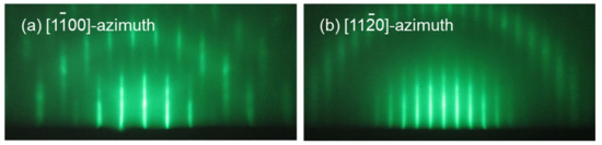
Figure 1.
Reflection high-energy electron diffraction RHEED images of Cr2O3 layer with (a) [] and (b) [] azimuth.
X-ray reflection (XRR) measurement was carried out to confirm the well-defined stacking structure. The XRR profile shown in Figure 2a shows the clear oscillation above 2θ/ω of 14°, which proves the sharp interfaces and the well-defined stacking structure. The FFT analysis of the oscillation gives the actual Cr2O3 thickness as 31.6 nm. In the high-angle X-ray diffraction (XRD) profile shown in Figure 2b, any diffraction peaks other than Pt(111) and α-Al2O3(0001) substrate were not observed. Many Laue fringes were observed around the Pt(111) diffraction peaks (Figure 2c), which indicate the good crystalline quality of the Pt buffer layer. It should be note that the diffraction peaks from the Cr2O3 layer are overlapped with those from the Pt(111)/Pt(222) diffraction peaks. The diffractions from the Cr2O3 layer could be masked because of the larger atomic scattering factor of Pt compared with Cr3+ and O2-.
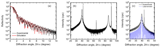
Figure 2.
(a) X-ray reflection (XRR), (b) high-angle 2θ/ω profile of the film. (c) represents the enlarged profile of (b) around 2θ/ω = 30-50°. Black and red lines in (a) represent the experimental result and the fitted result, respectively. Blue line in (c) represent the calculated profile using the Laue function.
Magnetic characterizations were carried out mainly by means of the AHE measurements after applying the ME field. For the AHE measurements, the film was patterned into the microdot with 15 μm diameter. On top of the microdot, the four top electrode (Cr/Au) was prepared by the lift-off technique. The optical microscope image with the electrical circuit is shown in Figure 3a. In our sample structure, the current flows in the Pt/Co/Au layer wherein the AHE detects the Co magnetization perpendicular to the film plane. This is suitable in this work because the studied film has the perpendicular magnetic anisotropy. In this work, the AHE loops were measured as a function of H applied to the direction perpendicular to the film. From the AHE loop, the exchange bias field, Hex, a shift of the magnetization curve along the H axis was evaluated. Hex was estimated as ∆HC/2 where HC is the switching field (coercivity) for up-to-down and down-to-up switching of the FM magnetization. E was applied between top (Pt/Co/Au) and bottom (Pt-buffer layer) electrodes, i.e., the direction perpendicular to film. The positive directions of H and E are defined as the direction from bottom (substrate side) to top (film side) of the film.
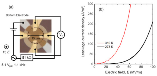
Figure 3.
(a) Optical microscope image of the device used for the test and the electric circuitry. (b) I-V curves of the Cr2O3 layer measured at 310 K (red) and 273 K (black).
Here, we denote the ME field as the simultaneously applied H and E because the energy gain by the ME effect ∆F is expressed as
∆F = αij·EiHj
Together with the crystallographic characterization of Cr2O3, the ME susceptibility evaluated in this paper is α33. As mentioned above, there are two typical processes to apply to the ME field: MEFC and isothermal modes. In the MEFC mode, the sample was once heated to above the Néel temperature of Cr2O3 (~307 K for bulk Cr2O3 [22]), 310 K. Then, HMEFC (μ0HMEFC = 5, 6, 7 T) and E (0–47 MV/m) were applied. In maintaining both fields, the sample was cooled to the AHE measurement temperature, 250 K at which the exchange bias polarity was checked. After measuring the AHE loop, the above heating and cooling processes were repeated with the different ME field condition. More details of the MEFC process can be found in [7,12].
In the isothermal process, the temperature kept constant during the ME field application and the AHE measurements. In this process, the sample was cooled from 310 K to 273 K under the H (μ0H = 0.6 T) application during the cooling: the conventional field-cooling (FC) to induce the exchange bias. At the constant temperature (273 K), Hisothermal (μ0Hisothermal = 6 T) and E (−60 – +100 MV/m) were simultaneously applied typically for 30 s. After that, E was removed and the AHE as a function of H measured. In the isothermal process, the sequential ME field application is important so that the exchange bias switching occurs accompanied by the hysteresis. In this work, the ME fields were applied in the following sequences.
- ME field application: for example, μ0Hisothermal = 6 T and E = +60 MV/m;
- Removing E and AHE measurement as a function of μ0H;
- ME field application: for example, μ0Hisothermal = 6 T and E = +80 MV/m;
- Removing E and AHE measurement as a function of μ0H;
These processes were repeated with increasing E until the exchange bias polarity is fully switched. Finally, after the exchange bias polarity was switched, the sign of the ME field was reversed, and the similar processes were repeated with the negative E.
- ME field application: for example, μ0Hisothermal = 6 T and E = 0 MV/m;
- Removing E and AHE measurement as a function of μ0H;
- ME field application, for example, μ0Hisothermal = 6 T and E = −18 MV/m;
- Removing E and AHE measurement as a function of μ0H;
- ME field application: for example, μ0Hisothermal = 6 T and E = −23 MV/m;
- Removing E and AHE measurement as a function of μ0H;
These processes were repeated with decreasing E until the exchange bias polarity is fully switched again. Details of the isothermal switching protocol can be found in our previous report [20]. Note that for both processes, the highest μ0H during the AHE loops was ±700 mT, which is low enough to switch the exchange bias polarity by H alone (|μ0H| > 8 T) [23].
3. Results and Discussions
Prior to showing the results on the ME-induced switching, it is helpful to show the electric resistance of the Cr2O3 layer. Using the same device used for the AHE measurements, the electric resistance was measured. Typical I-V curves measured at 310 K and 273 K are shown in Figure 3b. The I-V curves show the non-linear increase with respect to the voltage as is generally observed in an insulator thin film. Even at the most severe conditions adopted in this work (at highest temperature and at the highest E adopted), the current density is in the range of 102 A/m2, which is low enough compared with the current-induced magnetization switching, such as the spin-orbit torque mechanism, typically above 109 A/m2 [24,25].
First, we show the switching of the exchange bias polarity by the MEFC process. Figure 4a shows the series of AHE loops measured after the MEFC with μ0HMEFC = 7 T. When the electric field was not applied, e.g., the conventional FC, the negative exchange bias of μ0Hex = −108 mT appears (black curve). The similar AHE loops were obtained for E below 16 MV/m (blue curve). With increasing E, the step at about +100 mT starts to be observed in the AHE loop, a signature of the appearance of positive exchange bias. The two-step AHE loops are observed in the E range of 24–43 MV/m. The two-step magnetization curve is attributed to the co-existence of the positive and negative exchange biased domains. The similar two-step exchange biased state was observed in the previously reported ME-induced switching [16] and the magnetization curve after zero-field cooling [26]. The positive exchange bias grows with increasing E, the step at about −100 mT suppresses and instead, that at about +100 mT enhances. Finally, above E = 47 MV/m, the AHE loop shows the full positive exchange bias. In Figure 4b, the change in μ0Hex as a function of E during the MEFC is shown. We find that the change in the exchange bias is common to every μ0HMEFC. It should be noted that the AHE loops show the tiny hysteresis, i.e., the low coercivity. This is attributed to the usage of the Au spacer layer instead of the Pt spacer layer as in [21]. The Au spacer layer is suitable to tune the interfacial magnetic anisotropy in maintaining high exchange bias with suppressing the coercivity enhancement. The details of the role on the spacer layer can be found in our previous paper [21].
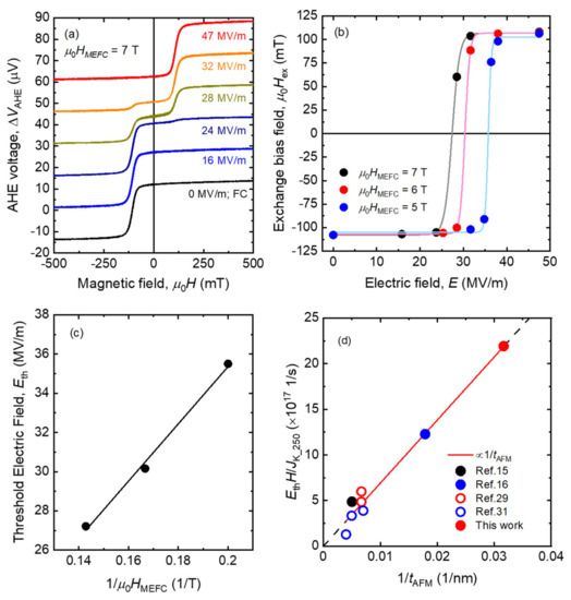
Figure 4.
(a) Anomalous Hall effect (AHE) loops as a function of μ0H after the magnetoelectric field cooling (MEFC). The E value for the MEFC are 0 (black), 16 MV/m (blue), 24 MV/m (dark blue), 28 MV/m (yellow), 32 MV/m (orange), and 47 MV/m (red). For every case, μ0HMEFC was 7 T. (b) Change in the exchange bias field with E. Black, red and blue point correspond to the case of μ0HMEFC = 7 T, 6 T and 5 T. Lines represent the fitted results using Equations (2) and (3). (c) Change in the threshold E with 1/μ0HMEFC. Line represents the linearly fitted result. (d) 1/tAFM dependence of the required EH product to switch the exchange bias. The EH values are normalized by the exchange anisotropy energy density at 250 K (see text).
The growth of the positive exchange-biased state by E is understood by the energy competition between JINT and the energy gain by the ME effect (Equation (1)) [27]. The former is caused by the interfacial exchange coupling between FM (Co) and interfacial AFM (Cr) spins. Previously, we reported that Co and interfacial Cr spins couples antiferromagnetically; the spin orientation of Co and interfacial Cr is opposite [28]. Under the positive HMEFC adopted in this paper, upward Co spin and downward Cr spin are the favorable spin alignments near the interface. When E during the MEFC is weak, this effect predominantly determines the interfacial spin alignment and yields the negative exchange-biased state. Conversely, the energy gain by the ME effect expressed by Equation (1) favors the upward Cr spin orientation favoring the positive exchange-biased state, which competes JINT. The phenomenological expression of this energy competition is given by [27]
where JINT denotes the interfacial exchange coupling energy (J/m2), tAFM is the AFM layer thickness (m), MAFM is the uncompensated AFM moment in the Cr2O3 layer (Wb/m2) and VAFM is the activation volume (m3) In the MEFC process, the spin configuration and the consequent exchange-biased state are determined during the cooling. Hence, the thermal fluctuation is also taken into account. Assuming that the fraction of the negative and positive exchange-biased state obeys the Boltzmann distribution, the change in the exchange bias should be expressed as [27]
where kB is a Boltzmann constant (J/K) and T is an absolute temperature (K). In Figure 4b, the fitted results using Equation (3) are shown as the solid lines. The results for all adopted MEFC conditions follow the same mathematical form. When HMEFC decreases, the curve shifts toward the high E. This shift can be also understood based on Equation (2). For the weaker HMEFC, the higher E is required to compensate JINT/tAFM. According to this argument, the required E to switch the exchange bias should be inversely proportional to HMEFC. Defining the threshold E, Eth to switch the exchange bias as E at which μ0Hex becomes zero, we plot the Eth as a function of 1/μ0HMEFC in Figure 4c. The Eth linearly increases with 1/H, which is in agreement with the above argument that the driving force for switching derives from the energy difference shown in Equation (1). The slope of Figure 4c gives the required EH product, which has been used as a measure of the ME-induced switching [15,27,29], as 1.24 × 10¹⁴ V·A/m2.
In other multiferroic systems such as BiFeO3, the cross-correlation coefficient such as the piezoelectric coefficient (d33) can be deteriorated with decreasing thickness because of the lattice confinement by the epitaxial strain [30]. Here, we discuss the deterioration/enhancement of α33 with reducing tAFM by comparing the obtained value with the previous reports for the similar FM/Cr2O3 stacked system [15,16,29,31]. To compare the EH product, JINT in Equation (2) has to be taken into account. Although the direct evaluation of JINT is difficult, the exchange anisotropy energy density JK (= Hex·MS·tFM) can be used as a measure of JINT; in the simple pinned spin model [32] or the weak JINT limit in the domain wall model [33], JINT and JK become equal to each other. Because JK depends on the temperature, JK measured at 250 K, JK_250 is used as a measure of JINT as in the previous paper [16]. To evaluate JK, the saturation magnetization per unit area, MS·tFM was measured based on the magnetization curve (M-H curve). The MS_FM·tFM value is (5.7 ± 0.7) × 10−10 Wb/m, which is higher than the bulk Co because of the sizable spin polarization of Pt and Au attached with Co [21]. In Figure 4d, the relationship between Eth·HMEFC/JK and tAFM is shown. As expected from Equation (2), Eth·HMEFC/JK roughly proportional to 1/tAFM. Notably, the Eth·H/JK–1/tAFM relationship is maintained up to the 30-nm-thickness regime, which suggests that α33 does not deteriorate in this thickness regime. This finding is in agreement that the switching is not highly influenced by the strain effect discussed above.
We further evaluate the α33 value based on the isothermal switching mode. Figure 5a shows the AHE loops after applying the ME fields, μ0Hisothermal = 6 T and E = +98 MV/m (red curve) and μ0Hisothermal = 6 T and E = −41 MV/m (blue curve), which correspond to the positive and the negative exchange-biased states, respectively. We find that the switching between two states reversibly occurs. Figure 5b shows the change in μ0Hex as a function of E. The clear hysteresis is observed, which indicates the presence of the energy barrier to switch the exchange bias polarity. We also find that the hysteresis shifts along the E-axis toward the positive direction, resembling the exchange bias in the M-H curve.
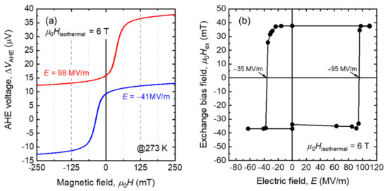
Figure 5.
(a) AHE loops as a function of μ0H after the applying the magnetoelectric (ME) fields in an isothermal way. Blue and red curves represent the AHE loop after applying E = +98 MV/m and −41 MV/m with μ0Hisothermal = 6 T, respectively. (b) Change in the exchange bias field as a function of E with μ0Hisothermal = 6 T. In (b), the threshold electric field is shown by text.
We analyze the shift of the hysteresis based on the phenomenological expression of the switching energy assuming the coherent rotation of the AFM spin. The switching ME condition is expressed as [20]
where KAFM denote the magnetic anisotropy energy density of the AFM layer (J/m3). In this expression, the change in the sing of α33 was taken into account. The sing of the second term depends on the switching direction: the negative-to-positive switching and the positive-to-negative switching. According to Equation (4), the asymmetry of the coercive E in the μ0Hex-E hysteresis is relevant to the difference in the switching energy caused by the unidirectional nature of JINT. Hence, the shift of the μ0Hex-E hysteresis is essentially same as JK. JK is quantified as
The first expression is the difference in the Zeeman energy for up-to-down and down-to-up switching of the FM magnetization. Values of MS_FM·tFM, (5.7 ± 0.7) × 10−10 Wb/m, and the exchange bias field Hex = ∆HC/2 obtained from the AHE loop yields JK at 273 K of 0.017 ± 0.002 mJ/m2. Because the exchange bias polarity is determined by the interfacial AFM spin direction [12], the μ0Hex-E hysteresis represents that of the interfacial AFM spin as a function of E. The second expression relies on this fact. Using JK, μ0Hisothermal (6 T), tAFM (31.6 nm, determined by XRR, see above) and ∆Eth (95−35 = 60 MV/m), α33 is yielded as 3.7 ± 0.5 ps/m. This value is in good agreement with the reported values at the same temperature for the bulk Cr2O3 and 500-nm-thick Cr2O3 film [6], ~4 ps/m.
One may imagine that the magnetic anisotropy energy of Cr2O3 can be evaluated from the KAFM value. In our experiments, the exchange bias was checked at zero E, i.e., after removing the ME field. Besides, the exchange bias polarity is determined by the interfacial AFM spin direction [12]. Considering them, the change in the exchange bias reflects the interfacial antiferromagnetic spin direction at the remanent state after applying the ME field. Hence, the physical meaning of the μ0Hex-E curve is similar to the remanent magnetization curve for the interfacial antiferromagnetic spin. The remanent magnetization curve is often used in the field of magnetic recording/storage and the details of the remanent magnetization curve can be found in [34]. Equation (4) assumes the coherent rotation whereas the switching occurs with the AFM domain wall motion [12]. In this case, the KAFM evaluated using Figure 5b and Equation (4) corresponds the ME energy equivalent to the remanent coercive E, which is typically two or three orders lower than the magnetocrystalline anisotropy energy density. This is similar to the fact that the switching H (the coercivity) in the M-H loop is different from the magnetic anisotropy field, 2KFM/MS_FM of the FM layer (KFM is a magnetic anisotropy energy density of FM layer).
Finally, we discuss the role of MAFM and the approach to decrease the switching energy using MAFM. As shown in Figure 4d, the reduction in tAFM enhances the switching energy, and this tendency is common to the isothermal mode. According to Equations (2) and (4), if MAFM is parallel to α33H, it would assist the switching. MAFM can be attributed to the finite magnetization at the bulk site [35,36] and/or the interfacial uncompensated moment [20]. The former relies on the defect-induced magnetization [35] and/or the selective substitution of the non-magnetic element such as Al to one sub-lattice [36]. Although the reduction effect using MAFM has been actually reported for the MEFC mode [28], the validity for the isothermal mode has not been proven, which will be investigated in the near future.
4. Conclusions
In summary, we investigate the ME-induced switching of the exchange bias, using especially the Cr2O3 thin film with the 30-nm thickness regime. While the previous reports seem to pay less attention to the isothermal reversible switching because of the difficulty, this switching mode as well as the MEFC-driven switching are demonstrated. Based on the argument on the switching energy, the non-deterioration of the ME susceptibility α33 in the studied thickness regime is found. The quantitative analysis based on the asymmetric switching energy in the isothermal switching gives the similar α33 value to the reported one for the bulk Cr2O3. While the cross-correlation functionality can deteriorate with decreasing thickness in some multiferroic materials, the finding in this paper could be a light for the further reduction in the ME-based all-thin-film system, which may be useful in spintronic applications.
Author Contributions
Conceptualization, Y.S. and R.N.; sample fabrication, Y.T.; data curation, Y.T. and K.T.; formal analysis, Y.S., Y.T. and K.T.; writing—original draft preparation, Y.S.; writing—review and editing, R.N.; funding acquisition, Y.S. All authors have read and agreed to the published version of the manuscript.
Funding
This research was partly funded by JSPS KAKENHI, grant number 19H00825.
Data Availability Statement
The study did not report any data.
Conflicts of Interest
The authors declare no conflict of interests. The funders had no role in the design of the study; in the collection, analysis, or interpretation of data; in the writing of the manuscript, or in the decision to publish the results.
References
- Wadley, P.; Howell, B.; Želeney, J.; Andrews, C.; Hills, V.; Campion, V.; Novák, V.; Olejník, K.; Maccherozzi, F.; Dhesi, S.; et al. Electrical switching of an antiferromagnet. Science 2016, 351, 587–590. [Google Scholar] [CrossRef] [PubMed]
- Astrov, D.N. The magnetoelectric effect in antiferromagnetics. Sov. Phys. JETP 1960, 11, 708–709. [Google Scholar]
- Folen, V.J.; Rado, G.T.; Stadler, E.W. Anisotropy of the magnetoelectric effect in Cr2O3. Phys. Rev. Lett. 1960, 6, 607–608. [Google Scholar] [CrossRef]
- Martin, T.J.; Anderson, J.C. Antiferromagnetic domain switching in Cr2O3. IEEE Trans. Magn. 1966, MAG 2, 446–449. [Google Scholar] [CrossRef]
- Iyama, A.; Kimura, T. Magnetoelectric hysteresis loops in Cr2O3 at room temperature. Phys. Rev. B 2013, 87, 180408. [Google Scholar] [CrossRef]
- Borisov, P.; Ashida, T.; Nozaki, T.; Sahashi, M.; Lederman, D. Magnetoelectric properties of 500-nm Cr2O3 films. Phys. Rev. B 2016, 93, 174415. [Google Scholar] [CrossRef]
- Borisov, P.; Hochstrat, A.; Chen, X.; Kleemann, W.; Binek, C. Magnetoelectric switching of exchange bias. Phys. Rev. Lett. 2005, 94, 117203. [Google Scholar] [CrossRef]
- Kosub, T.; Kopte, M.; Radu, F.; Schmidt, O.G.; Makarov, D. All-electric access to the magnetic-field-invariant magnetization of antiferromagnets. Phys. Rev. Lett. 2015, 115, 097201. [Google Scholar] [CrossRef] [PubMed]
- Chen, X.; Hochstrat, A.; Borisov, P.; Kleemann, W. Magnetoelectric exchange bias systems in spintronics. Appl. Phys. Lett. 2006, 89, 202508. [Google Scholar] [CrossRef]
- Toyoki, K.; Shiratsuchi, Y.; Nakamura, T.; Mitsumata, C.; Harimoto, S.; Takechi, Y.; Nishimura, T.; Nomura, H.; Nakatani, R. Equilibrium surface magnetization of α-Cr2O3 studied through interfacial chromium magnetization in Co/α-Cr2O3 layered structures. Appl. Phys. Express 2014, 7, 114210. [Google Scholar] [CrossRef]
- Ashida, T.; Oida, M.; Shimomura, N.; Nozaki, T.; Shibata, T.; Sahashi, M. Observation of magnetoelectric effect in Cr2O3/Co thin film system. Appl. Phys. Lett. 2014, 104, 152409. [Google Scholar] [CrossRef]
- Shiratsuchi, Y.; Watanabe, S.; Yoshida, H.; Kishida, N.; Nakatani, R.; Kotani, Y.; Toyoki, K.; Nakamura, T.; Nakatani, R. Observation of the magnetoelectric reversal process of the antiferromagnetic domain. Appl. Phys. Lett. 2018, 113, 242404. [Google Scholar] [CrossRef]
- Ashida, T.; Oida, M.; Shimomura, M.; Nozaki, T.; Shibata, T.; Sahashi, M. Isothermal electric switching of magnetization in Cr2O3/Co thin film system. Appl. Phys. Lett. 2015, 106, 132407. [Google Scholar] [CrossRef]
- Hui, Y.; Lin, W.; Xie, Q.; Chen, S.; Miao, X.; Chen, J. Magnetoelectric effect of epitaxial Cr2O3 thin films with a conducting underlayer electrode. J. Phys. D Appl. Phys. 2019, 52, 24LT03. [Google Scholar] [CrossRef]
- Shiratsuchi, Y.; Nakatani, R. Perpendicular exchange bias and magneto-electric control using Cr2O3(0001) thin film. Mater. Trans. 2016, 57, 781–788. [Google Scholar] [CrossRef]
- Shiratsuchi, Y.; Toyoki, K.; Tao, Y.; Aono, H.; Nakatani, R. Realization of magnetoelectric effect in 50-nm-thick Cr2O3 thin film. Appl. Phys. Express 2020, 13, 043003. [Google Scholar] [CrossRef]
- Wang, J.-L.; Echtenkamp, W.; Mahmood, A.; Binek, C. Voltage controlled magnetism in Cr2O3 based all-thin-film systems. J. Magn. Magn. Mater. 2019, 486, 165262. [Google Scholar] [CrossRef]
- Mitsumata, C.; Sakuma, A.; Fukamichi, K.; Tsunoda, M.; Takahashi, M. Critical thickness of antiferromagnetic layer in exchange biasing bilayer system. J. Phys. Soc. Jpn. 2008, 77, 044602. [Google Scholar] [CrossRef]
- Kota, Y.; Imamura, H. Narrowing of antiferromagnetic domain wall in corundum-type Cr2O3 by lattice strain. Appl. Phys. Express 2017, 10, 013002. [Google Scholar] [CrossRef]
- Nguyen, T.V.A.; Shiratsuchi, Y.; Yonemura, S.; Shibata, T.; Nakatani, R. Energy condition of isothermal magnetoelectric switching of perpendicular exchange bias in Pt/Co/Au/Cr2O3/Pt stacked film. J. Appl. Phys. 2018, 124, 233902. [Google Scholar] [CrossRef]
- Shiratsuchi, Y.; Kuroda, W.; Nguyen, T.V.A.; Kotani, Y.; Toyoki, K.; Nakamura, T.; Suzuki, M.; Nakamura, K.; Nakatani, R. Simultaneous achievement of high perpendicular exchange bias and low coercivity by controlling ferromagnetic/antiferromagnetic interfacial magnetic anisotropy. J. Appl. Phys. 2017, 121, 073902. [Google Scholar] [CrossRef]
- Foner, S. High-field antiferromagnetic resonance in Cr2O3. Phys. Rev. 1963, 130, 183–197. [Google Scholar] [CrossRef]
- Shiratsuchi, Y.; Wakatsu, K.; Nakamura, T.; Oikawa, H.; Maenou, S.; Narumi, Y.; Tazoe, K.; Mitsumata, C.; Kinoshita, T.; Nojiri, H.; et al. Isothermal switching of perpendicular exchange bias by pulsed high magnetic field. Appl. Phys. Lett. 2012, 100, 262413. [Google Scholar] [CrossRef]
- Jungwirth, T.; Marti, X.; Wadley, P.; Wunderlich, J. Antiferromagnetic spintronics. Nat. Nanotechnol. 2016, 11, 231. [Google Scholar] [CrossRef] [PubMed]
- Baltz, V.; Manchon, A.; Tsoi, M.; Moriyama, T.; Ono, T.; Tserkovnyak, Y. Antiferromagnetic spintronics. Rev. Mod. Phys. 2018, 90, 015005. [Google Scholar] [CrossRef]
- Jia, J.; Chen, Y.; Wang, B.; Han, B.; Wu, Y.; Wang, Y.; Cao, J. The double-shifted magnetic hysteresis loops and domain structure in perpendicular [Co/Ni]N/IrMn exchange biased systems. J. Phys. D Appl. Phys. 2019, 52, 065001. [Google Scholar] [CrossRef]
- Toyoki, K.; Shiratsuchi, Y.; Kobane, A.; Mitsumata, C.; Kotani, Y.; Nakamura, T.; Nakatani, R. Magnetoelectric switching of perpendicular exchange bias in Pt/Co/Pt/α-Cr2O3/Pt stacked films. Appl. Phys. Lett. 2015, 106, 162404. [Google Scholar] [CrossRef]
- Al-Mahdawi, M.; Pati, S.P.; Shiokawa, Y.; Ye, S.; Nozaki, T.; Sahashi, M. Low-energy magnetoelectric control of domain satte in exchange-coupled heterostructures. Phys. Rev. B 2017, 95, 144423. [Google Scholar] [CrossRef]
- Shiratsuchi, Y.; Noutomi, H.; Oikawa, H.; Nakamura, T.; Suzuki, M.; Fujita, T.; Arakawa, K.; Takechi, Y.; Mori, H.; Kinoshita, T.; et al. Detection and in situ switching of unreversed interfacial antiferromagnetic spins in a perpendicular exchange biased system. Phys. Rev. Lett. 2012, 109, 077202. [Google Scholar] [CrossRef]
- Wang, J.; Neaton, J.B.; Zheng, H.; Nagarajan, V.; Ogale, S.B.; Liu, B.; Viehland, D.; Vaithyarathan, V.; Schlom, D.G.; Waghmare, U.V.; et al. Epitaxial BiFeO3 multiferroic thin film heterostructures. Science 2003, 299, 1719–1722. [Google Scholar] [CrossRef]
- Shiratsuchi, Y.; Toyoki, K.; Nakatani, R. Magnetoelectric control of antiferromagnetic domain state in Cr2O3 thin film. J. Phys. Condensed Matter. 2021, submitted. [Google Scholar]
- Meiklejohn, W.H. Exchange anisotropy—A review. J. Appl. Phys. 1962, 33, 1328–1335. [Google Scholar] [CrossRef]
- Mauri, D.; Siegmann, H.C.; Bagus, P.S.; Kay, E. Simple model for thin ferromagnetic films exchange coupled to an antiferromagnetic substrate. J. Appl. Phys. 1987, 62, 3047–3049. [Google Scholar] [CrossRef]
- Bertotti, G. Hysteresis in Magnetism; Academic Press: San Diego, CA, USA, 1998; pp. 17–20. [Google Scholar]
- Kosub, T.; Kopte, M.; Hühne, R.; Appel, P.; Shields, B.; Maletinsky, P.; Hübner, R.; Liedke, M.O.; Schimidt, O.G.; Makarov, D. Purely antiferromagnetic magnetoelectric random access memory. Nat. Commun. 2016, 8, 13985. [Google Scholar] [CrossRef] [PubMed]
- Nozaki, T.; Al-Mahdawi, M.; Shiokawa, Y.; Pati, S.P.; Ye, S.; Kotani, Y.; Toyoki, K.; Nakamura, T.; Suzuki, M.; Yonemura, S.; et al. Manipulation of antiferromagnetic spin using tunable parasitic magnetization in magnetoelectric antiferromagnet. Phys. Status Solidi RRL 2018, 12, 180366. [Google Scholar] [CrossRef]


Publisher’s Note: MDPI stays neutral with regard to jurisdictional claims in published maps and institutional affiliations. |
© 2021 by the authors. Licensee MDPI, Basel, Switzerland. This article is an open access article distributed under the terms and conditions of the Creative Commons Attribution (CC BY) license (http://creativecommons.org/licenses/by/4.0/).