

Revisiting Multiple Ring Oscillator-Based True Random Generators to Achieve Compact Implementations on FPGAs for Cryptographic Applications

 ,
,  ,
,  , and
, and
Abstract
1. Introduction
2. Previous Work
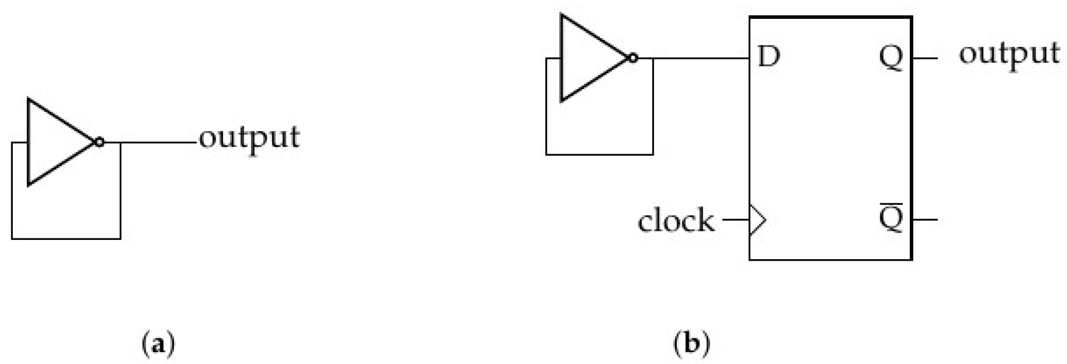
3. Study of a Basic Sampled RO
- Frequency test (Frequency): Analyzes the proportion of ‘0’s and ‘1’s for the entire sequence. This proportion should be 1/2, and each sequence to be tested should have bits.
- Frequency Test within a Block (Block Frequency): Analyzes the proportion of ‘0’s and ‘1’s within M-bit blocks. In this case, n should be bits, and the block size M should be such that , , and , where .
- Cumulative Sums Test (Cumulative Sums): This test analyzes whether the cumulative sum of the partial sequences occurring in the tested sequence is too large or too small relative to the expected behavior. This test has two modes, depending on whether it is applied forward or backward through the input sequence. In this test, n should be bits.
- Runs Test (Runs): Analyzes the total number of “runs” in the sequence, where a run is a sequence of k identical bits. The purpose of this test is to determine whether the oscillation between ‘0’s and ‘1’s is too fast or too slow. The length of the sequence to analyze should be bits.
- Test for the Longest Run of Ones in a Block (Longest Run): This test analyzes the longest run of ones within -bit blocks, thus determining whether the length of the longest “run” of ‘1’s within the tested sequence corresponds to what is expected in a random sequence. It uses three preset values for M in terms of the number of bits n of the sequence: when , when 750,000, and when 750,000.
- Binary Matrix Rank Test (Rank): This test analyzes the linear dependence among fixed-length subsequences by determining the rank of disjoint submatrices of the entire sequence. The length of the sequence to analyze should be 38,912 bits.
- Discrete Fourier Transform Test (FFT): This test detects periodic features in the sequence by applying the Discrete FFT. The length of the sequence to be analyzed should be bits.
- Non-overlapping Template Matching Test (Non Overlapping): This test analyzes the number of occurrences of prespecified subsequences in order to detect too many occurrences of a given nonperiodic pattern. If the pattern is not found, the window slides one bit. For this test, the length of the templates should be or , and the length of the entire sequence, n, should be such that ( is recommended), , and .
- Overlapping Template Matching Test (Overlapping): This test is similar to the previous one, but in this case, the window slides when the pattern is found. For this test, the length of the templates should be or , and the length of the entire sequence should be .
- Maurer’s “Universal Statistical” Test (Universal): This test analyzes whether the sequence can be significantly compressed without loss of information. In that case, the sequence is considered not random. For this test, the sequence is divided into L-bit blocks, recommended to be , and 387,840. The concrete value of L depends on n, as specified in [29].
- Approximate Entropy Test (Approximate Entropy): This test analyzes the frequency of all possible overlapping -bit patterns across the entire sequence. For this test, n and should be such that .
- Random Excursions Test (Random Excursions): This test analyzes the number of cycles having a given number of visits in a cumulative sum random walk. A cycle of a random walk consists of a sequence of random steps of unit length that begin at and return to the origin. This test is composed of a series of eight tests, and it requires .
- Random Excursions Variant Test (Random Excursions Variant): This test analyzes the total number of times that a particular state is visited in a cumulative sum random walk. This test is composed of a series of eighteen tests, and it requires .
- Serial Test (Serial): In this test, the frequency of all possible overlapping -bit patterns across the entire sequence is analyzed. n and should be such that .
- Linear Complexity Test (Linear): In this test, linear-feedback shift registers (LFSRs) of length are built to check the linear complexity of the generated sequence. For this test, must be in the range of , and the length of the entire sequence should be .
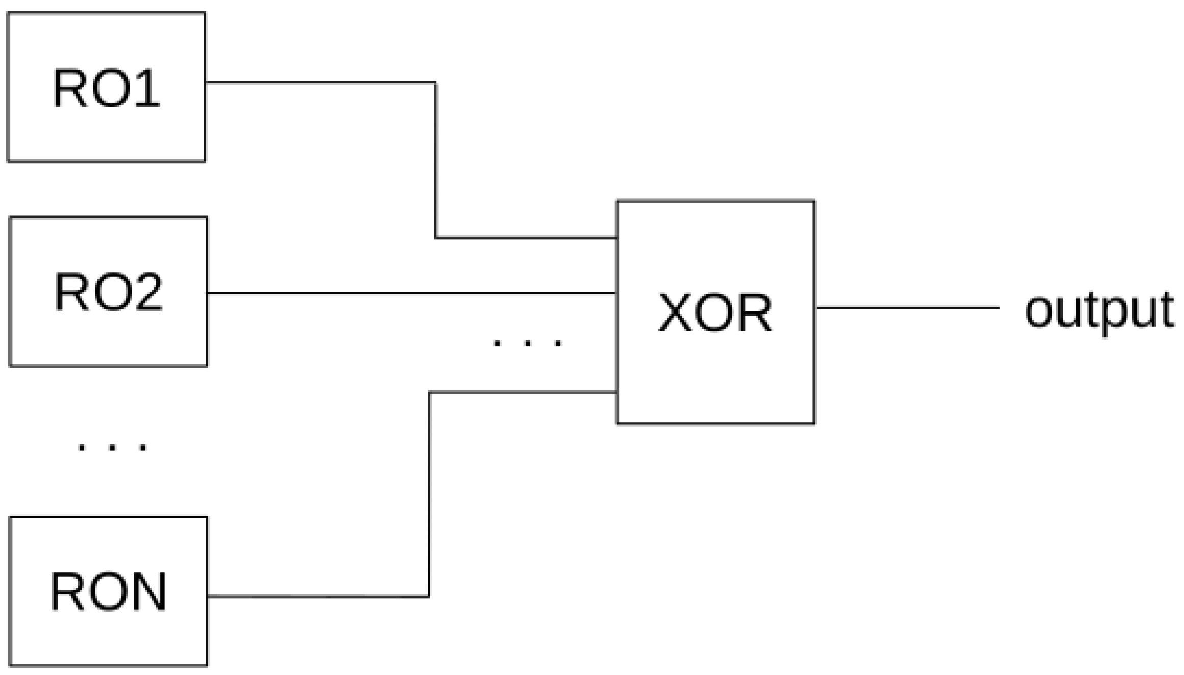
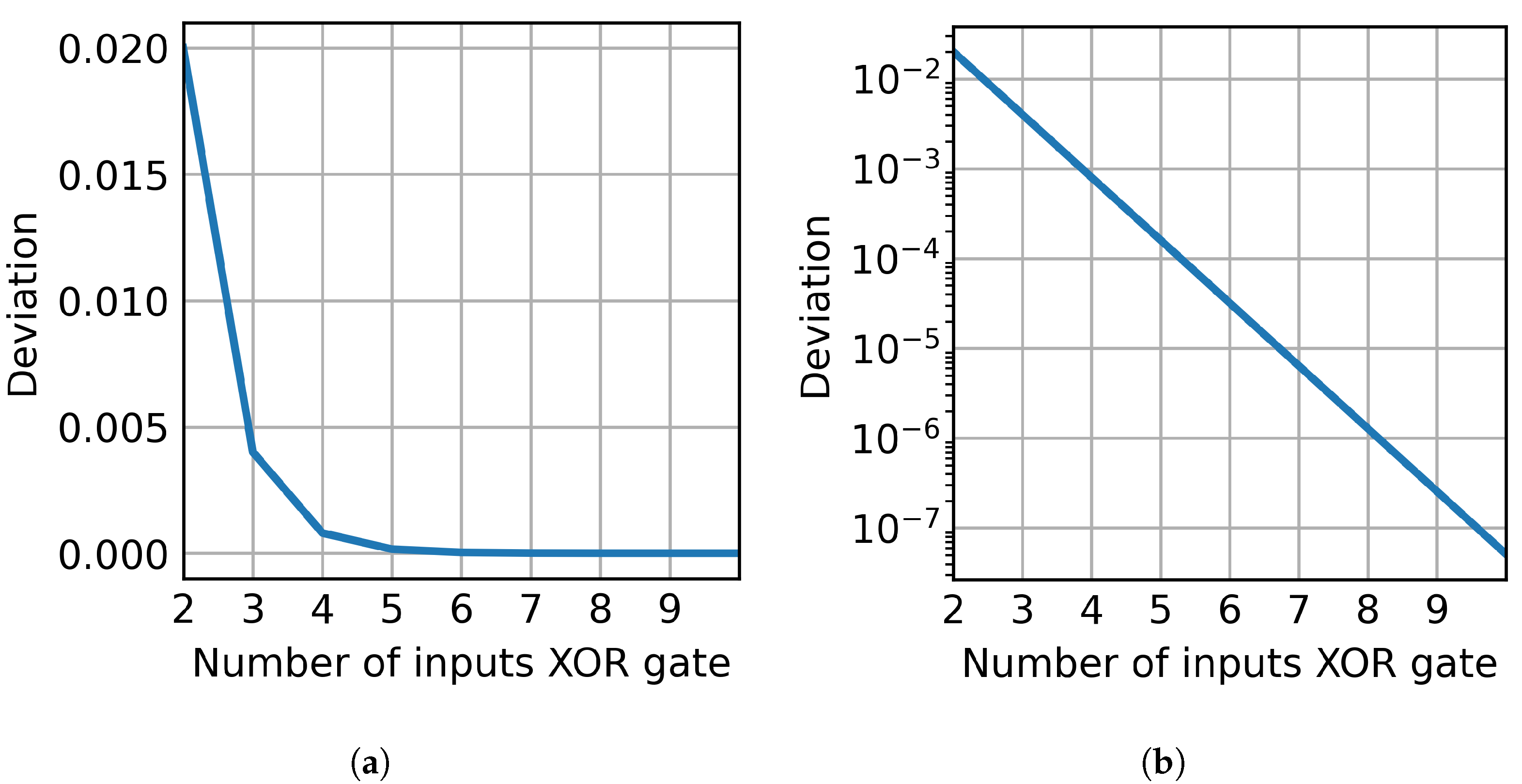
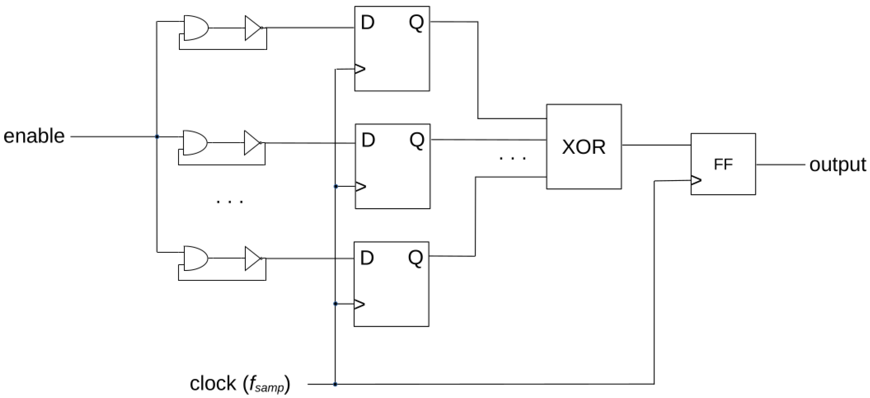
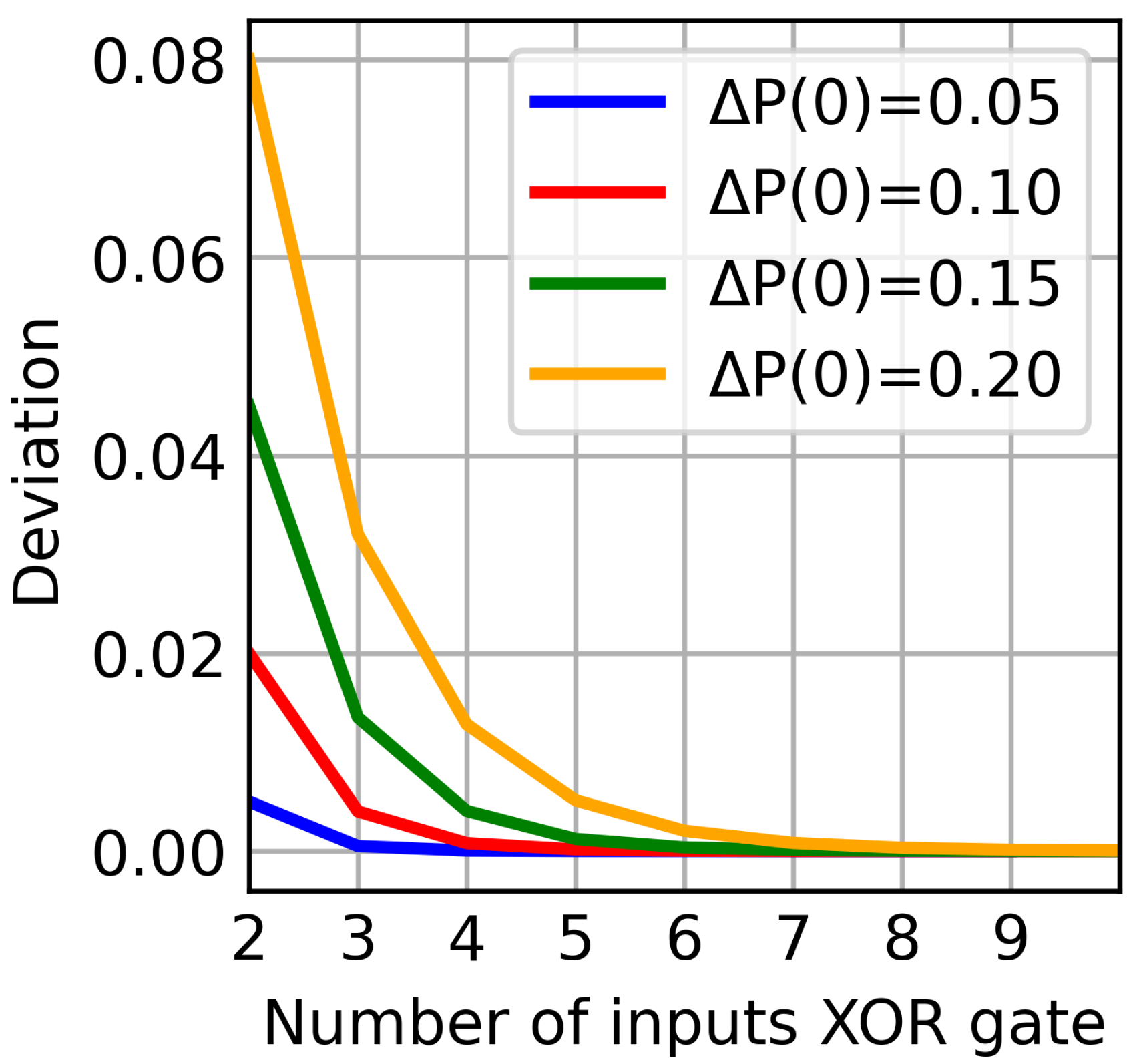
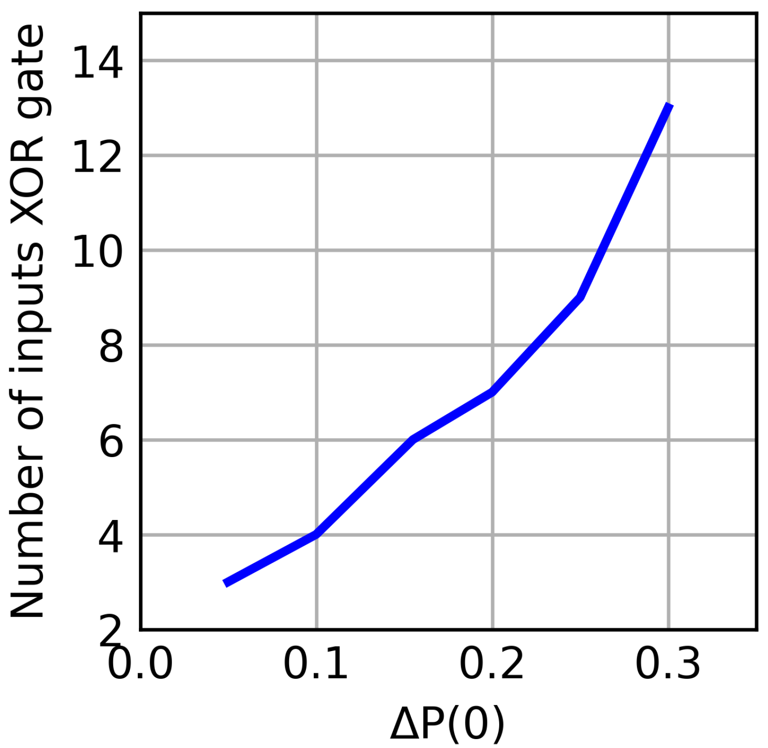
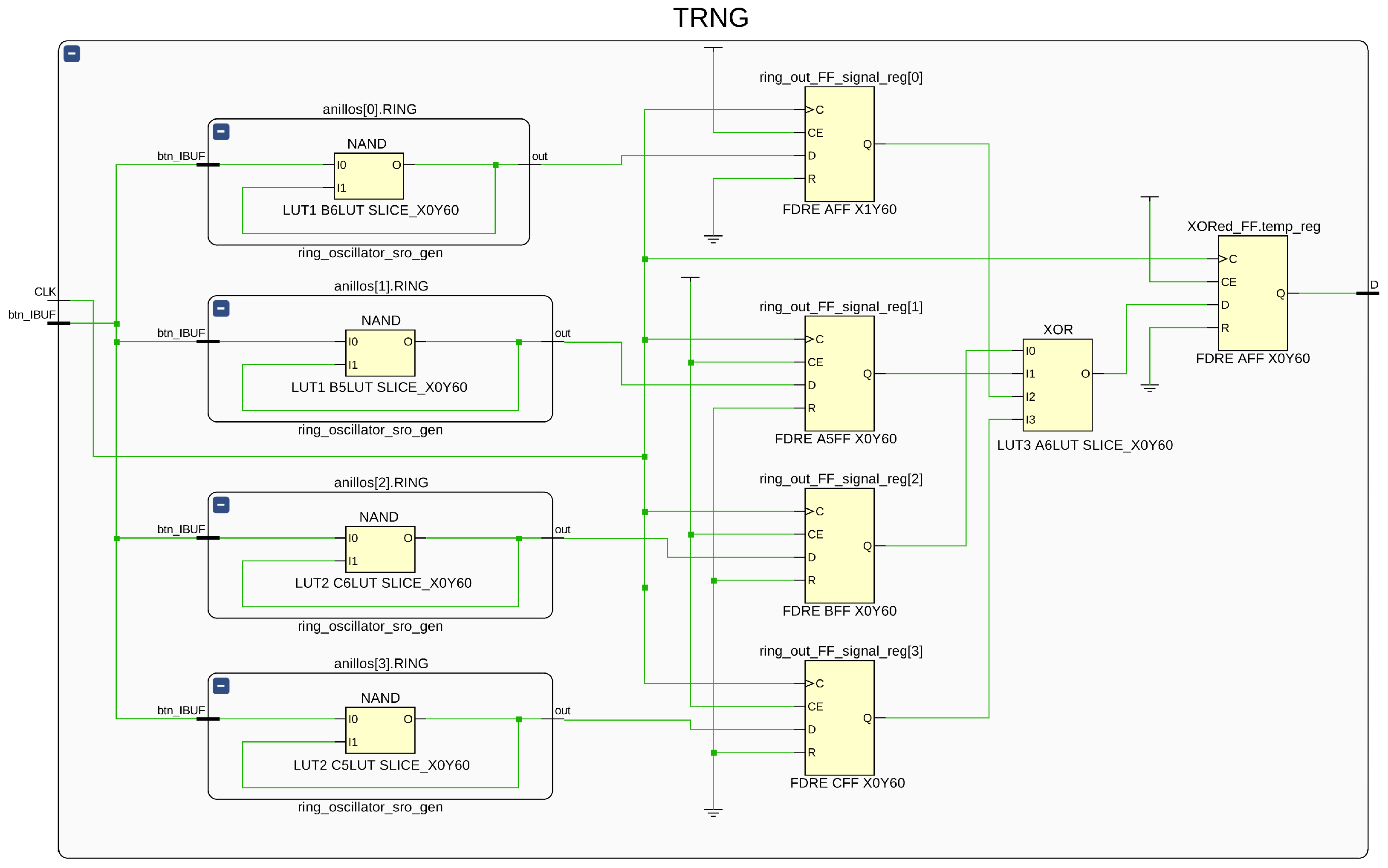
4. Multiple XORed Ring Oscillators
- 1.
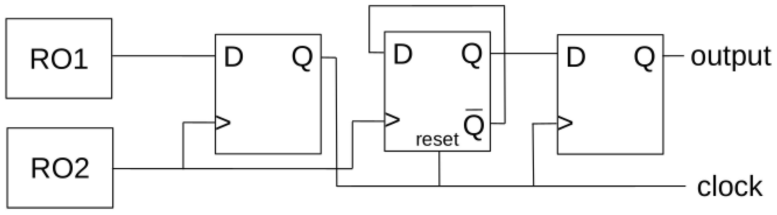
- Implement a SARO(1)-FF ring oscillator operating at the target sampling frequency corresponding to the desired throughput, following the scheme in Figure 5.
- 2.
- Capture a bitstream with a statistically significant size (), and analyze the frequency of ‘0’s and ‘1’s. The frequency test from the NIST suite can be used for this purpose. From this analysis, estimate the deviation probability of ‘0’s, .
- 3.
- 4.
- 5.
- In case NIST tests are not passed, increment N and go to 4.
5. Comparison to Other TRNGs for FPGAs
6. Conclusions
Author Contributions
Funding
Data Availability Statement
Conflicts of Interest
References
- Hull, T.E.; Dobell, A.R. Random number generators. SIAM Rev. 1962, 4, 230–254. [Google Scholar] [CrossRef]
- Bright, H.S.; Enison, R.L. Quasi-random number sequences from a long-period TLP generator with remarks on application to cryptography. Acm Comput. Surv. (CSUR) 1979, 11, 357–370. [Google Scholar] [CrossRef]
- Gutmann, P. Software Generation of Practically Strong Random Numbers. In Proceedings of the Usenix Security Symposium 1998, San Antonio, TX, USA, 26–29 January 1998. [Google Scholar]
- Jun, B.; Kocher, P. The Intel Random Number Generator. Cryptography Research, Inc. White Paper Prepared for Intel Corporation. 1999, Volume 27, pp. 1–8. Available online: https://www.rambus.com/wp-content/uploads/2015/08/IntelRNG.pdf (accessed on 9 May 2023).
- Raj, H.; Saroiu, S.; Wolman, A.; Aigner, R.; Cox, J.; England, P.; Fenner, C.; Kinshumann, K.; Loeser, J.; Mattoon, D.; et al. ftpm: A Firmware-Based tpm 2.0 Implementation. Microsoft Research. 2015. 23p. Available online: https://www.microsoft.com/en-us/research/publication/ftpm-a-firmware-based-tpm-2-0-implementation/ (accessed on 9 May 2023).
- Tidrea, A.; Korodi, A.; Silea, I. Cryptographic considerations for automation and SCADA systems using trusted platform modules. Sensors 2019, 19, 4191. [Google Scholar] [CrossRef]
- Morán, A.; Parrilla, L.; Roca, M.; Font-Rosselló, J.; Isern, E.; Canals, V. Digital implementation of Radial Basis Function Neural Networks based on Stochastic Computing. IEEE J. Emerg. Sel. Top. Circuits Syst. 2023, 13, 257–269. [Google Scholar] [CrossRef]
- Parrilla, L.; Castillo, E.; López-Ramos, J.A.; Álvarez-Bermejo, J.A.; García, A.; Morales, D.P. Unified compact ECC-AES co-processor with group-key support for IoT devices in wireless sensor networks. Sensors 2018, 18, 251. [Google Scholar] [CrossRef]
- Fischer, V.; Bernard, F.; Bochard, N.; Varchola, M. Enhancing security of ring oscillator-based TRNG implemented in FPGA. In Proceedings of the 2008 International Conference on Field Programmable Logic and Applications, Heidelberg, Germany, 8–10 September 2008; pp. 245–250. [Google Scholar]
- Petura, O.; Mureddu, U.; Bochard, N.; Fischer, V.; Bossuet, L. A survey of AIS-20/31 compliant TRNG cores suitable for FPGA devices. In Proceedings of the 2016 26th International Conference on Field Programmable Logic and Applications (FPL), Lausanne, Switzerland, 29 August–2 September 2016; pp. 1–10. [Google Scholar]
- Sivaraman, R.; Rajagopalan, S.; Amirtharajan, R. FPGA based generic RO TRNG architecture for image confusion. Multimed. Tools Appl. 2020, 79, 13841–13868. [Google Scholar] [CrossRef]
- Xu, X.; Wang, Y. High speed true random number generator based on FPGA. In Proceedings of the 2016 International Conference on Information Systems Engineering (ICISE), Los Angeles, CA, USA, 20–22 April 2016; pp. 18–21. [Google Scholar]
- Della Sala, R.; Bellizia, D.; Scotti, G. A novel ultra-compact FPGA-compatible TRNG architecture exploiting latched ring oscillators. IEEE Trans. Circuits Syst. II Express Briefs 2021, 69, 1672–1676. [Google Scholar] [CrossRef]
- Syafalni, I.; Jonatan, G.; Sutisna, N.; Mulyawan, R.; Adiono, T. Efficient homomorphic encryption accelerator With integrated PRNG using low-cost FPGA. IEEE Access 2022, 10, 7753–7771. [Google Scholar] [CrossRef]
- Bakiri, M.; Guyeux, C.; Couchot, J.F.; Oudjida, A.K. Survey on hardware implementation of random number generators on FPGA: Theory and experimental analyses. Comput. Sci. Rev. 2018, 27, 135–153. [Google Scholar] [CrossRef]
- Isaacs, J.C.; Watkins, R.K.; Foo, S.Y. Cellular automata PRNG: Maximal performance and minimal space FPGA implementations. Eng. Appl. Artif. Intell. 2003, 16, 491–499. [Google Scholar] [CrossRef]
- Amano, H. Principles and Structures of FPGAs; Springer: Cham, Switzerland, 2018. [Google Scholar]
- Vasyltsov, I.; Hambardzumyan, E.; Kim, Y.S.; Karpinskyy, B. Fast digital TRNG based on metastable ring oscillator. In Proceedings of the Cryptographic Hardware and Embedded Systems–CHES 2008: 10th International Workshop, Washington, DC, USA, 10–13 August 2008; Springer: Cham, Switzerland, 2008; pp. 164–180. [Google Scholar]
- Maiti, A.; Casarona, J.; McHale, L.; Schaumont, P. A large scale characterization of RO-PUF. In Proceedings of the 2010 IEEE International Symposium on Hardware-Oriented Security and Trust (HOST), Anaheim, CA, USA, 13–14 June 2010; pp. 94–99. [Google Scholar]
- Baudet, M.; Lubicz, D.; Micolod, J.; Tassiaux, A. On the security of oscillator-based random number generators. J. Cryptol. 2011, 24, 398–425. [Google Scholar] [CrossRef]
- Kohlbrenner, P.; Gaj, K. An embedded true random number generator for FPGAs. In Proceedings of the 2004 ACM/SIGDA 12th International Symposium on Field Programmable Gate Arrays, Monterey, CA, USA, 22–24 February 2004; pp. 71–78. [Google Scholar]
- Sunar, B.; Martin, W.J.; Stinson, D.R. A provably secure true random number generator with built-in tolerance to active attacks. IEEE Trans. Comput. 2006, 56, 109–119. [Google Scholar] [CrossRef]
- Wold, K.; Tan, C.H. Analysis and enhancement of random number generator in FPGA based on oscillator rings. Int. J. Reconfigurable Comput. 2009, 2009, 4. [Google Scholar] [CrossRef]
- Parrilla, L.; García, A.; Castillo, E.; Álvarez-Bermejo, J.A.; López-Villanueva, J.A.; Meyer-Baese, U. Dracon: An Open-Hardware Based Platform for Single-Chip Low-Cost Reconfigurable IoT Devices. Electronics 2022, 11, 2080. [Google Scholar] [CrossRef]
- Parrilla, L.; García, A.; Castillo, E.; Rodríguez-Bolívar, S.; López-Villanueva, J.A. Time-and Amplitude-Controlled Power Noise Generator against SPA Attacks for FPGA-Based IoT Devices. J. Low Power Electron. Appl. 2022, 12, 48. [Google Scholar] [CrossRef]
- Parrilla, L.; Castillo, E.; Todorovich, E.; Morales, D.; Botella, G.; Garcia, A. Improvements for the applicability of power-watermarking to embedded IP cores protection: E-coreIPP. Digit. Signal Process. 2015, 44, 110–122. [Google Scholar] [CrossRef]
- Xilinx Inc. 7 Series FPGAs Family Overview. Available online: https://docs.xilinx.com/v/u/en-US/ds180_7Series_Overview (accessed on 18 April 2022).
- Pareschi, F.; Rovatti, R.; Setti, G. On statistical tests for randomness included in the NIST SP800-22 test suite and based on the binomial distribution. IEEE Trans. Inf. Forensics Secur. 2012, 7, 491–505. [Google Scholar] [CrossRef]
- Rukhin, A.; Soto, J.; Nechvatal, J.; Smid, M.; Barker, E. A Statistical Test Suite for Random and Pseudorandom Number Generators for Cryptographic Applications; Technical Report; Booz-Allen and Hamilton Inc.: Mclean, VA, USA, 2001. [Google Scholar]
- Xilinx Inc. Spartan-6 FPGA Data Sheet: DC and Switching Characteristics. Available online: https://docs.xilinx.com/v/u/en-US/ds162 (accessed on 18 April 2023).
- Xilinx Inc. Artix-7 FPGAs Data Sheet: DC and AC Switching Characteristics. Available online: https://docs.xilinx.com/v/u/en-US/ds181_Artix_7_Data_Sheet (accessed on 18 April 2023).
- Xilinx Inc. 7 Series FPGAs Configurable Logic Block. Available online: https://docs.xilinx.com/v/u/en-US/ug474_7Series_CLB (accessed on 18 April 2023).
- Anandakumar, N.N.; Sanadhya, S.K.; Hashmi, M.S. FPGA-based true random number generation using programmable delays in oscillator-rings. IEEE Trans. Circuits Syst. II Express Briefs 2019, 67, 570–574. [Google Scholar] [CrossRef]
- Wang, X.; Liang, H.; Wang, Y.; Yao, L.; Guo, Y.; Yi, M.; Huang, Z.; Qi, H.; Lu, Y. High-throughput portable true random number generator based on jitter-latch structure. IEEE Trans. Circuits Syst. I Regul. Pap. 2020, 68, 741–750. [Google Scholar] [CrossRef]
- Frustaci, F.; Spagnolo, F.; Perri, S.; Corsonello, P. A High-Speed FPGA-based True Random Number Generator using Metastability with Clock Managers. IEEE Trans. Circuits Syst. II Express Briefs 2022, 70, 756–760. [Google Scholar] [CrossRef]


| Test Name | p-Value | Pass-Rate 1 | Result |
|---|---|---|---|
| Frequency | 0.000000 | 0% | ✘ |
| Block Frequency | 0.000000 | 1% | ✘ |
| Cumulative Sums 2 | [0.000000, 0.000000] | [0, 0]% | ✘ |
| Runs | 0.000000 | 0% | ✘ |
| Longest Run | 0.000000 | 0% | ✘ |
| Rank | 0.153763 | 99% | ✓ |
| FFT | 0.000000 | 68% | ✓ |
| Non Overlapping 2 | [0.000000, 0.911413] | [0, 100]% | ✘ |
| Overlapping | 0.000000 | 2% | ✘ |
| Universal | 0.017912 | 98% | ✓ |
| Approximate Entropy | 0.000000 | 89% | ✘ |
| Random Excursions 2 | — | — | ✘ |
| Random Excursions Variant 2 | — | — | ✘ |
| Serial 2 | [0.000000, 0.699313] | [89, 98]% | ✘ |
| Linear Complexity | 0.137282 | 98% | ✓ |
| Test Name | p-Value | Pass-Rate 1 | Result |
|---|---|---|---|
| Frequency | 0.000000 | 6% | ✘ |
| Block Frequency | 0.000000 | 66% | ✘ |
| Cumulative Sums 2 | [0.000000, 0.000000] | [6, 6]% | ✘ |
| Runs | 0.000000 | 38% | ✘ |
| Longest Run | 0.330628 | 98% | ✓ |
| Rank | 0.311542 | 99% | ✓ |
| FFT | 0.199580 | 96% | ✓ |
| Non Overlapping 2 | [0.000006, 0.980883] | [93, 100]% | ✘ |
| Overlapping | 0.000003 | 100% | ✘ |
| Universal | 0.013808 | 98% | ✓ |
| Approximate Entropy | 0.000398 | 98% | ✓ |
| Random Excursions 2 | — | — | ✘ |
| Random Excursions Variant 2 | — | — | ✘ |
| Serial 2 | [0.151616, 0.894201] | [98, 98]% | ✓ |
| Linear Complexity | 0.739918 | 100% | ✓ |
| Design | k | LUTs + FFs | ||
|---|---|---|---|---|
| SARO(0)-FF | 0 (1 NAND, 0 NOT) | 1 + 1 | ||
| SARO(1)-FF | 1 (1 AND, 1 NOT) | 2 + 1 | ||
| SARO(2)-FF | 2 (1 NAND, 2 NOT) | 3 + 1 | ||
| SARO(3)-FF | 3 (1 AND, 3 NOT) | 4 + 1 |
| Test Name | p-Value | Pass-Rate 1 | Result |
|---|---|---|---|
| Frequency | 0.001112 | 100% | ✓ |
| Block Frequency | 0.289667 | 98% | ✓ |
| Cumulative Sums 2 | [0.249284, 0.834308] | [100, 100]% | ✓ |
| Runs | 0.987896 | 99% | ✓ |
| Longest Run | 0.383827 | 99% | ✓ |
| Rank | 0.798139 | 99% | ✓ |
| FFT | 0.319084 | 99 % | ✓ |
| Non Overlapping 2 | [0.000134, 0.991468] | [96, 100]% | ✓ |
| Overlapping | 0.678686 | 99% | ✓ |
| Universal | 0.637119 | 98% | ✓ |
| Approximate Entropy | 0.334538 | 98% | ✓ |
| Random Excursions 2 | [0.009535, 0.924076] | [96, 100]% | ✓ |
| Random Excursions Variant 2 | [0.055361, 0.946308] | [98, 100]%% | ✓ |
| Serial 2 | [ 0.040108, 0.739918] | [99, 100]% | ✓ |
| Linear Complexity | 0.145326 | 100% | ✓ |
| Design | N | LUTs | FFs | Slices | NIST Tests | |
|---|---|---|---|---|---|---|
| MX-3-SARO | 50 kHz | 3 | 3 | 4 | 1 | ✘ |
| MX-3-SARO | 40 kHz | 3 | 3 | 4 | 1 | ✘ |
| MX-3-SARO | 33 kHz | 3 | 3 | 4 | 1 | ✓ |
| MX-4-SARO | 50 kHz | 4 | 3 | 5 | 2 | ✓ |
| MX-4-SARO | 50 kHz | 4 | 7 | 5 | 2 | ✓ |
| MX-4-SARO | 100 kHz | 4 | 7 | 5 | 2 | ✓ |
| Design | Throughput | LUTs | Power Consumption | Device |
|---|---|---|---|---|
| [33] | 6 Mbps | 528 (LUT4) | - | Spartan 3A |
| [34] | 100 Mbps | 56 | 1.5 mW * | Virtex 6 |
| [35] | 300 Mbps | 38 | 119 mW | Zynq 7000 |
| [23] (25 ROs) | 100 Mbps | 83 (LUT4) | - | Ciclone II |
| [23] (50 ROs) | 100 Mbps | 167 (LUT4) | - | Ciclone II |
| MX-4-SARO | 100 Kbps | 7 | 41 mW | Artix 7 |
| MX-4-SARO | 50 Kbps | 3 | 40 mW | Artix 7 |
| MX-3-SARO | 33 Kbps | 3 | 25mW | Artix 7 |
Disclaimer/Publisher’s Note: The statements, opinions and data contained in all publications are solely those of the individual author(s) and contributor(s) and not of MDPI and/or the editor(s). MDPI and/or the editor(s) disclaim responsibility for any injury to people or property resulting from any ideas, methods, instructions or products referred to in the content. |
© 2023 by the authors. Licensee MDPI, Basel, Switzerland. This article is an open access article distributed under the terms and conditions of the Creative Commons Attribution (CC BY) license (https://creativecommons.org/licenses/by/4.0/).
Share and Cite
Parrilla, L.; García, A.; Castillo, E.; López-Villanueva, J.A.; Meyer-Baese, U. Revisiting Multiple Ring Oscillator-Based True Random Generators to Achieve Compact Implementations on FPGAs for Cryptographic Applications. Cryptography 2023, 7, 26. https://doi.org/10.3390/cryptography7020026
Parrilla L, García A, Castillo E, López-Villanueva JA, Meyer-Baese U. Revisiting Multiple Ring Oscillator-Based True Random Generators to Achieve Compact Implementations on FPGAs for Cryptographic Applications. Cryptography. 2023; 7(2):26. https://doi.org/10.3390/cryptography7020026
Chicago/Turabian StyleParrilla, Luis, Antonio García, Encarnación Castillo, Juan Antonio López-Villanueva, and Uwe Meyer-Baese. 2023. "Revisiting Multiple Ring Oscillator-Based True Random Generators to Achieve Compact Implementations on FPGAs for Cryptographic Applications" Cryptography 7, no. 2: 26. https://doi.org/10.3390/cryptography7020026
APA StyleParrilla, L., García, A., Castillo, E., López-Villanueva, J. A., & Meyer-Baese, U. (2023). Revisiting Multiple Ring Oscillator-Based True Random Generators to Achieve Compact Implementations on FPGAs for Cryptographic Applications. Cryptography, 7(2), 26. https://doi.org/10.3390/cryptography7020026