Article

Detour-RS: Reroute Attack Vulnerability Assessment with Awareness of the Layout and Resource †

Department of Electrical and Computer Engineering, University of Florida, Gainesville, FL 32611, USA
*
Author to whom correspondence should be addressed.
This paper is an extended version of our paper published in 2023 IEEE International Symposium on Hardware Oriented Security and Trust (HOST).
Cryptography 2024, 8(2), 13; https://doi.org/10.3390/cryptography8020013
Submission received: 21 October 2023 / Revised: 30 March 2024 / Accepted: 2 April 2024 / Published: 6 April 2024
(This article belongs to the Special Issue Feature Papers in Hardware Security II)

Abstract

:
Recent decades have witnessed a remarkable pace of innovation and performance improvements in integrated circuits (ICs), which have become indispensable in an array of critical applications ranging from military infrastructure to personal healthcare. Meanwhile, recent developments have brought physical security to the forefront of concern, particularly considering the valuable assets handled and stored within ICs. Among the various invasive attack vectors, micro-probing attacks have risen as a particularly menacing threat. These attacks leverage advanced focused ion beam (FIB) systems to enable post-silicon secret eavesdropping and circuit modifications with minimal traceability. As an evolved variant of micro-probing attacks, reroute attacks possess the ability to actively disable built-in shielding measures, granting access to the security-sensitive signals concealed beneath. To address and counter these emerging challenges, we introduce a layout-level framework known as Detour-RS. This framework is designed to automatically assess potential vulnerabilities, offering a systematic approach to identifying and mitigating exploitable weaknesses. Specifically, we employed a combination of linear and nonlinear programming-based approaches to identify the layout-aware attack costs in reroute attempts given specific target assets. The experimental results indicate that shielded designs outperform non-shielded structures against reroute attacks. Furthermore, among the two-layer shield configurations, the orthogonal layout exhibits better performance compared to the parallel arrangement. Furthermore, we explore both independent and dependent scenarios, where the latter accounts for potential interference among circuit edit locations. Notably, our results demonstrate a substantial near 50% increase in attack cost when employing the more realistic dependent estimation approach. In addition, we also propose time and gas consumption metrics to evaluate the resource consumption of the attackers, which provides a perspective for evaluating reroute attack efforts. We have collected the results for different categories of target assets and also the average resource consumption for each via, required during FIB reroute attack.

1. Introduction

Over the last few decades, there has been a remarkable advancement in integrated circuit (IC) technology, fueling a broad set of applications ranging from lightweight terminals to advanced data centers and even future quantum computing [1]. This results in a substantial boost in computational power and seamless connectivity among smart devices, which form the backbone of modern technology and society. While the semiconductor industry has thrived during this period, the concerns with respect to hardware security have grown significantly because of a wide range of physical attack vectors, which can be roughly classified into three categories, i.e., non-invasive, semi-invasive, and invasive attacks, as illustrated in Figure 1. The difference between these categories lies in the requirements of (chip) sample preparations. Non-invasive attacks such as the well-known power/EM side-channel attacks [2] and fault injection attacks [3] are mostly plug-and-play, i.e., without mandating package/silicon preparations. For instance, power side-channel attacks can deduce the underlying cryptographic keys by solely analyzing the run-time power variations of sensitive operations, while clock glitch-based fault injection attacks only manipulate the clock signals to affect the design timing paths instead of impacting the hardware devices physically. As for semi-invasive attack vectors like optical probing or optical fault injection, adversaries typically tend to remove the package and/or thin the silicon substrate such that the optical energy can be available or penetrate into the device at a specific range of wavelengths. Optical probing techniques have also been demonstrated to derive on-chip FPGA bitstream decryption keys on 28 nm Xilinx devices [4]. Along with attacks of higher levels like bitstream reverse engineering [5,6], adversaries can enable more fine-grained and sophisticated compromises on the entire system. When it comes to invasive attacks, they represent a family of much stronger and extremely effective mechanisms as these attacks can exploit advanced equipment to access more details of devices under analysis physically. For example, hardware reverse engineering solutions may be able to extract complete physical layouts from silicon dies.
In the realm of invasive attack techniques, focused ion beam (FIB)-based micro-probing attacks [7,8] are gaining increasing attention within both academic and industrial circles. These attacks are noteworthy for their unique capability to intrude upon and manipulate the inner workings of a manufactured electronic circuit with minimal disruption to the overall system.
FIB-based probing attacks become particularly relevant in scenarios where physical access to the IC is compromised. This can occur in various real-world situations, such as the following:
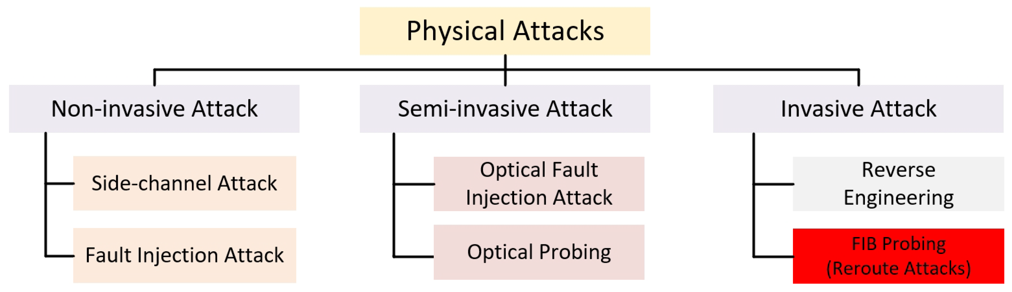
  • Reverse engineering: When an adversary gains access to the physical IC, he/she may attempt to reverse engineer the design and functionality of the device using FIB-based techniques. This poses a threat to intellectual property and proprietary information.
  • Counterfeiting and tampering: FIB-based probing can be employed to modify or tamper with the IC at the silicon level. This is a concern in applications where the integrity and authenticity of the IC are critical, such as in secure microcontrollers or cryptographic devices.
  • Hardware security modules: In the context of hardware security modules, where sensitive cryptographic operations are performed, FIB-based attacks could potentially compromise the confidentiality and integrity of cryptographic keys.
  • Defense and aerospace applications: In sectors like defense and aerospace, where security is paramount, unauthorized access to and tampering with ICs through FIB-based attacks could have severe consequences, including the compromise of mission-critical systems.
More precisely, FIB technology possesses the remarkable capability to precisely remove and apply materials at a nano-scale level, allowing for extremely fine-grained modifications. This unique attribute enables exceptionally precise interventions and alterations in electronic circuits after the silicon fabrication process. An illustrative example of a security breach involves the replication of a physical unclonable function (PUF) based on static random-access memory (SRAM) [9]. In this instance, a FIB was employed to meticulously etch a segment of the SRAM’s transistors, creating a bias that enables attackers to forecast the initialization during start-up and compel the system to adopt predetermined configurations. Other attack cases include those aimed at extracting sensitive plaintext data, compromising private cryptographic keys, and accessing security tokens [10].
For example, designers can place active shield nets at the top metal layers during the design time. As such, potential probing intrusions might compromise the active metal wires that continuously transfer specific pattern signals; the mismatch between the information from the top-layer metal wires and reference signals underneath can be detected to trigger the subsequent countermeasures against micro-probing attacks [11,12]. In addition, analog sensors like the probe attempt detector (PAD) [13] can capture the added capacitance and delay imposed by the attached probe in a timely manner. However, these existing solutions either suffer from exorbitant overhead or low reliability, failing to become a silver bullet to address threats. Taking the challenge of securing against invasive micro-probing attacks further, an advanced variant known as the reroute attack has emerged, presenting an even more concerning threat. This variant is designed to effectively neutralize the shield-protection mechanisms, making it easier to access sensitive signals compared to conventional bypass attacks [14]. The essence of the reroute attack lies in a cunning strategy—it involves the deliberate destruction of a portion of the protective shield while simultaneously introducing FIB intrusion at an alternate location. By adopting this approach, attackers can clandestinely gain access to critical nets within the design without triggering detection mechanisms. This covert maneuver poses a serious challenge to hardware security, highlighting the need for heightened vigilance and innovative countermeasures in an era where attackers continue to evolve their techniques to compromise sensitive systems. In this research endeavor, we strive to gain deeper insights into the emerging threat landscape posed by reroute attacks. To this end, we present a comprehensive layout-aware assessment framework, called Detour-RS, specially designed to evaluate the susceptibility of ICs at the physical design level. Our framework empowers designers with the means to perform efficient and precise quantification of an IC’s vulnerability to reroute attacks. (This paper is an extended version, which includes our newly developed metric, layout-aware added trace length, and deploys the hybrid optimization utilizing the combination of linear and nonlinear programming approaches to obtain more accurate results. We presented the new results with a hybrid optimization approach, and we also compared the time cost during the calculation. In addition, we developed time and gas consumption metrics to evaluate the reroute attack efforts in terms of the gas and time consumption during the FIB editing to gain a complete understanding of the resource consumption of the attackers.) The contributions of this study are multifaceted, encompassing the following key aspects:
  • We introduce an advanced and meticulously automated security assessment framework that operates with a keen awareness of layout intricacies. This framework is tailored to assess the vulnerabilities within design layouts when subjected to the latest FIB precision techniques. Our proposed solution stands at the forefront of automation, providing a comprehensive evaluation of layout vulnerabilities in the context of reroute attacks, aligning seamlessly with the state-of-the-art capabilities of FIB technology.
  • Our research has resulted in the development of an innovative metric, the layout-aware added traces’ length. This metric quantifies the effort required for the reroute attacks. Our solution seamlessly integrates both linear and nonlinear programming techniques into our framework. It automates the identification of circuit edit locations within shield nets, forming the basis for reroute path establishment and streamlining the process.
  • We conducted a comprehensive series of experiments using various physical design layouts for a system-on-chip (SoC) design, employing our Detour-RS framework. Our findings indicate that a two-layer shield structure offers greater resilience against reroute attacks compared to a single-layer design. Additionally, within the context of two-layer shield protection, an orthogonal configuration exhibited higher resistance than a parallel one. These insights underscore the potential benefits of particular layout choices for enhancing the security of intricate SoC designs.
  • We propose time and gas consumption metrics to evaluate the resource consumption of the reroute attackers. The results are demonstrated for different sets of target assets, and we also obtained the average resource cost for each single via, which provides another fair perspective to evaluate the reroute attacks.
  • We methodically explored both independent and dependent scenarios, distinguishing mainly by whether circuit edits from reroute attacks are allowed to overlap or not. Our findings reveal a noteworthy observation: in the more practical dependent scenario, there is a nearly 50% increase in the demand for layout-aware added traces. Furthermore, we introduce a graphical tool that facilitates intuitive visualization of target asset exposure to reroute attacks, along with the associated statistical insights.
In addition to the overall contributions of our Detour-RS framework, we would like to spell out the extensions and improvements explicitly compared to our previous Detour framework in [15] as follows:
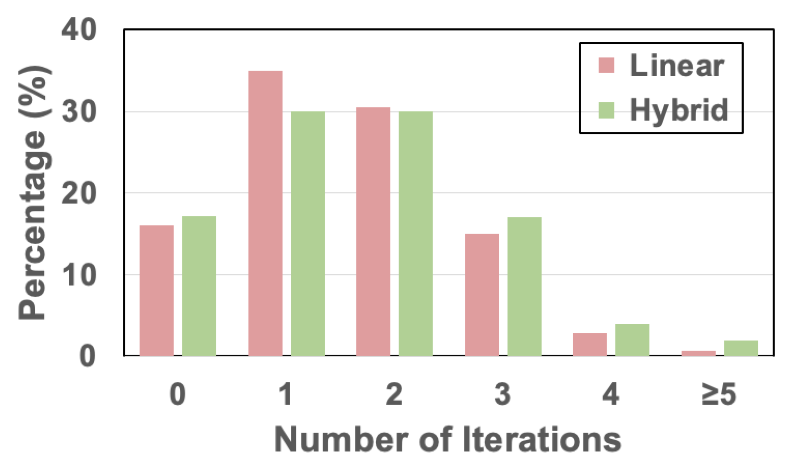
  • Improved simplicity and accuracy: We extend our linear programming-based approach in [31] to a hybrid model covering both linear and nonlinear scenarios such that the vulnerabilities of reroute attacks within the target layout can be analyzed in a more comprehensive and accurate manner. Although the linear programming we utilized previously can be effective in reroute attack vulnerability assessment, the linear constraints increase exponentially with respect to targets and associated shield nets. As such, the linear programming-based implementation in our original solution (i.e., Detour) is very tricky and error-prone since the discontinuous constraints involved need to be deliberately analyzed and attached under various intrusion scenarios. Missing single-corner cases can easily lead to suboptimal results, e.g., over-/under-estimating the vulnerabilities. In contrast, employing a general optimization methodology that can handle both linear and nonlinear problems can be very beneficial to alleviate the cumbersomeness of constraint creation because we only need to define the entire problem scope for gradient-based search, making the analysis more reliable and accurate.
  • Nonlinear problem coverage: As all linear programming problems are mathematically special cases of nonlinear problems, our hybrid model in Detour-RS can effectively address all cases of Detour (our conference version). In addition to the implementation perspective, we would like to highlight that using a hybrid model including nonlinear programming is not overkill in our case because the objective function, in some complicated scenarios, is better represented with a continuous, but nonlinear one. We present a specific example to illustrate how our extended hybrid model can address nonlinear scenarios in Section 5.1.
  • Time and gas metrics: Almost all existing works regarding reroute attacks or micro-probing attack vulnerability assessment focus on the exploitable windows of FIB intrusions, e.g., the exposed area metric in our framework. However, other factors can also play important roles in practical attack determination. It is worth mentioning that FIB is extremely precise and expensive equipment; the required time and gas resource consumption of reroute attacks thus reflect the feasibility and difficulty, serving as a useful reference for threat evaluation.
The subsequent sections of this paper are organized as follows to offer a comprehensive exploration of our research. In Section 2, we lay the foundation by providing in-depth background on micro-probing attacks and the existing countermeasures, shedding light on the evolving threat landscape. In Section 3, we delve into the heart of our research, presenting the Detour-RS framework in detail. This section not only elucidates the intricacies of our framework, but also elaborates on the innovative metrics we have developed for assessing reroute attacks and the workflow that enables their computation for any design layout. The empirical evidence and insights drawn from our experiments are presented in Section 4, offering a clear illustration of our framework’s effectiveness. Finally, we draw the threads together in Section 6, providing a comprehensive conclusion that encapsulates the contributions and implications of our research.

2. Background

This section begins with an introduction to FIB technology and its application in micro-probing attacks. Subsequently, we delve into the landscape of currently available assessment solutions and countermeasures that address probing attacks. Finally, we elucidate our threat model to provide a comprehensive understanding of the context.

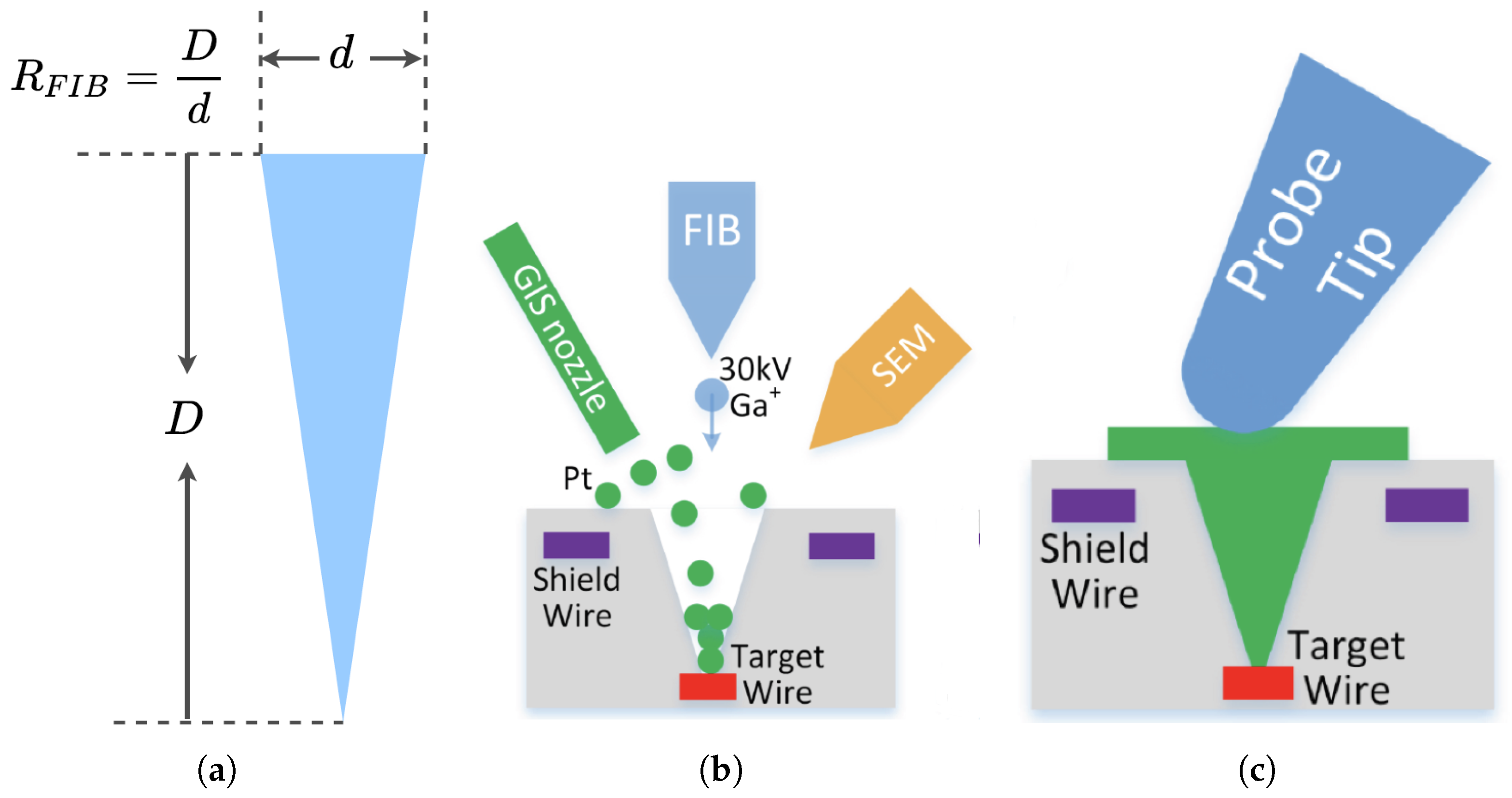
2.1. Basics of FIB-Based Micro-Probing

The application of focused ion beam (FIB) technology in integrated circuit (IC) editing has notably evolved, demonstrating its prowess as a versatile and precise tool. FIB’s capabilities extend to both the removal and deposition of materials within a fabricated chip, enabling intricate tasks such as cutting traces or establishing metal connections with pinpoint accuracy [16,17]. Additionally, FIB proves invaluable in the creation of probing points for electrical testing, facilitating fundamental tasks in electrical design characterization, redesign parameter verification, and the diagnosis of manufacturing faults and anomalies [18]. However, in the hands of adversaries wielding advanced FIB techniques, the potential for direct eavesdropping and the reconstruction of security-sensitive assets within ICs becomes a concerning reality. These assets may encompass critical components like confidential messages, decryption keys, or device configurations, thereby intensifying the security challenges faced by ICs [10].
In Figure 2, we provide a visual representation of the fundamental principles underlying focused ion beam (FIB)-based micro-probing attacks. In particular, Figure 2a highlights a critical parameter in FIB systems known as the aspect ratio, denoted as R F I B and defined as the ratio of the milling hole’s depth (D) to its diameter (d). Notably, the aspect ratio assumes significance in the context of FIB attacks. A larger aspect ratio indicates increased potency for adversaries, as it implies a narrower milling hole, which may bypass shield nets and evade detection systems.
The process of a FIB-based micro-probing attack typically unfolds as follows: After creating a hole through the IC package to access the sensitive metal wires using FIB, adversaries proceed with a sequence of steps, including metal deposition, dielectric deposition, and imaging of the IC, often utilizing a scanning electron microscope (SEM) for precise visualization (see Figure 2b). FIB systems are renowned for their capability to image, etch, and deposit materials on an IC with remarkable precision, achieved through a finely focused gallium ion (Ga+) beam with resolutions as fine as 4–5 nanometers. Some systems, utilizing helium or neon ions, offer even greater precision. The integration of a navigation system with FIB technology allows for the characterization of chip subsurface features, ensuring compliant circuit-level edits. High-energy Ga beams are employed to mill through conductors, while gases such as tungsten (W), platinum (Pt), or silicon dioxide are precisely deposited using an ion beam in coordination with an injection system (GIS) nozzle, depending on the required gas chemistry. This process establishes a conducting path from the sensitive signals, which can subsequently be accessed using an external probe tip to extract security assets (as demonstrated in Figure 2c). These intricate steps and precise capabilities of FIB systems underscore the potential security risks associated with micro-probing attacks, prompting the need for robust countermeasures.

2.2. FIB-Aware Anti-Probing Physical Design Flow

Figure 3 provides a comprehensive insight into the categorization of shield structures, which can generally be classified into two main categories: single-layer and multiple-layer. Within the realm of single-layer shields, two distinct configurations emerge, exemplified by ‘snake-like wires’, as depicted in Figure 3a, and ‘parallel wires’, showcased in Figure 3d. The ‘snake-like’ structure offers the advantage of requiring fewer driving signals to cover extensive sensitive areas, while the ‘parallel shield structure’ is noted for its potential resilience against advanced attacks, as discussed in [14].
When venturing into the territory of multiple-layer shield structures, three primary types garner consideration: orthogonal, parallel, and random shielding. To attain optimal protection, it is imperative to establish a minimum spacing between each shield net within the same layer. In the case of distinct-layer shield nets, an additional 50% offset relative to the pitch size may be incorporated into the lower layer shield within a two-layer parallel shield configuration. This design strategy is facilitated by the focused ion beam (FIB)-aware anti-probing physical design framework, iPROBE, as detailed in [9,14]. iPROBE empowers the integration of diverse shield structures, encompassing both single- and two-layer configurations, thus offering enhanced flexibility and adaptability in shielding against probing attacks.

2.3. Countermeasures
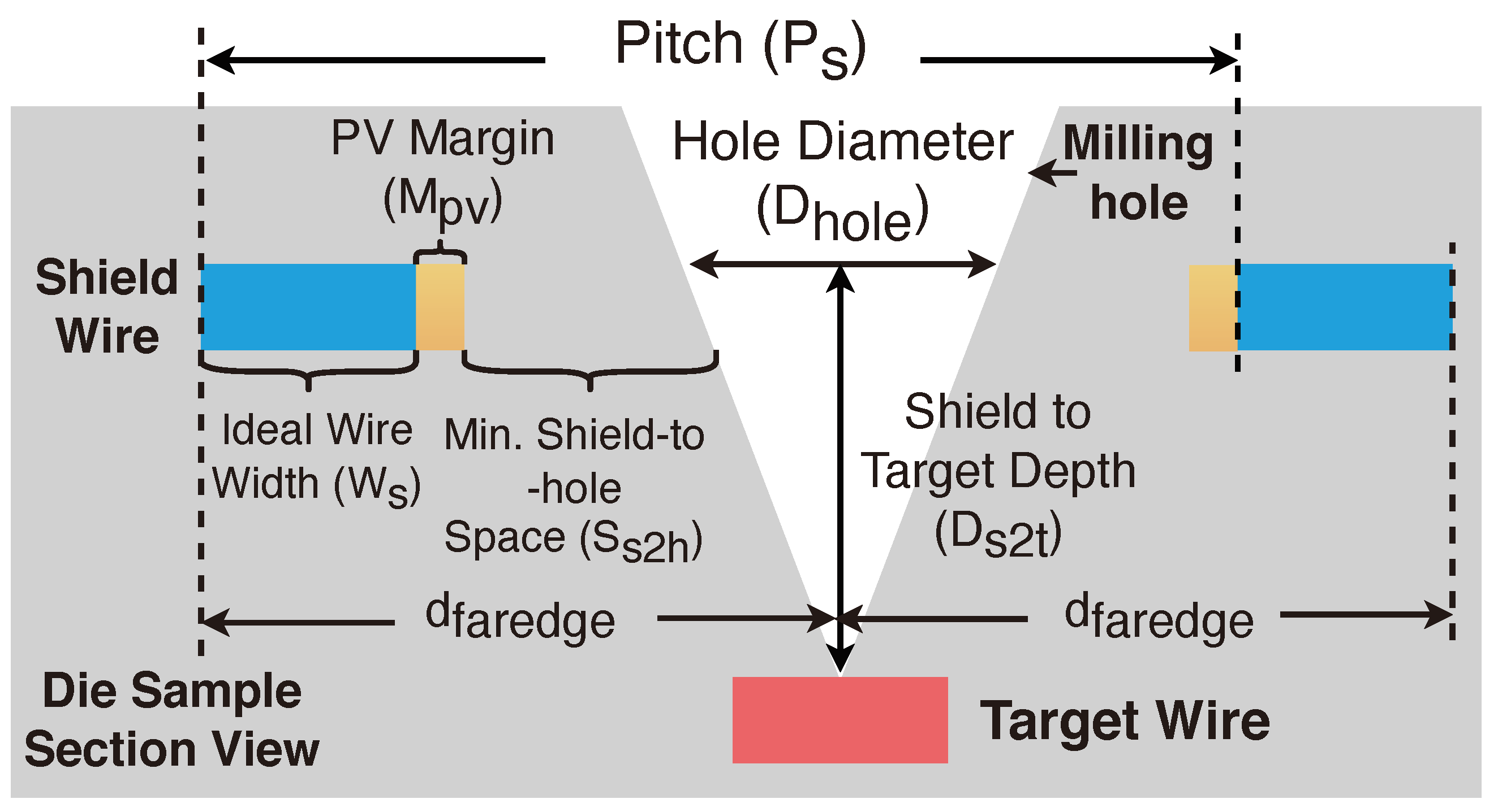
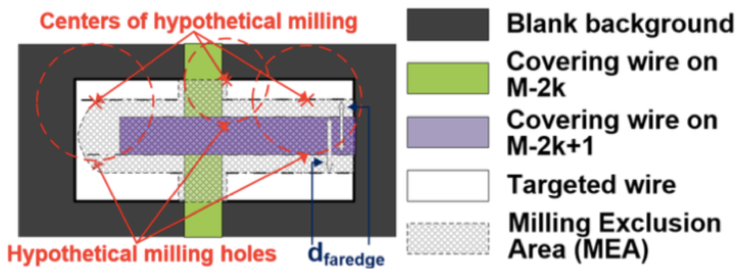
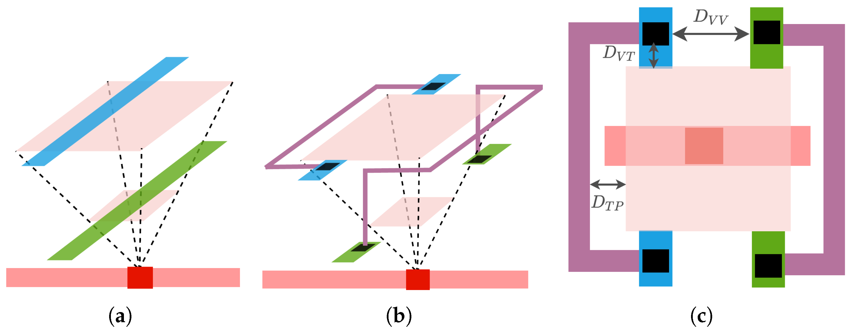
The first step of the typical probing attacks is to either partially or fully remove the chip package in order to expose the silicon die. Researchers have devised an array of strategies, such as physical protection and tamper resistance, specialized coatings, and layers for defense against FIB intrusion, which include secure enclosures [20,21] and tamper-evident packaging [22,23]. They did a great job of resisting FIB penetration and hindering attackers from reaching sensitive areas, yet they may be vulnerable to prolonged and sophisticated attacks that gradually breach the protective layers. Subsequently, the process involves extracting in-depth assets. This is achieved through iterative steps of delayering and imaging, which reveal the chip’s internal structure and its operational functions. Many countermeasures have been established, such as randomized logic and layouts to confound attackers [24,25,26] and cryptographic safeguards to secure sensitive data [27,28] and cryptographic keys. However, they can be resource-intensive and complex, potentially slowing down systems and requiring strong key management. Additionally, there are concerns like vulnerabilities in algorithms, depreciation of encryption standards, and performance overhead. Once the target nets for probing have been determined, the next task involves the identification of the corresponding metal wires’ location on the targeted IC. Secure debugging interface management is employed to restrict unauthorized access through debugging interfaces [29,30], though they might suffer from potential for increased complexity in debugging processes, additional hardware requirements, and potential performance overhead due to the added security measures.
Furthermore, FIB-based probing attacks can be categorized into two main types: bypass attack and reroute attack. They are primarily differentiated by their approach to circuit modification. A bypass attack occurs when attackers breach the shield nets’ gap space by creating a small opening without severing shield or alarm wires. Conversely, a reroute attack leverages the circuit editing capabilities of the FIB to establish a new path between equipotential points on the shield wire, effectively nullifying a significant portion of the shield’s protection.
There are a variety of countermeasures and evaluation approaches being proposed against FIB-based probing attacks. A variety of countermeasures and evaluation techniques have emerged to counter FIB-based probing attacks. For example, in [31], an anti-probing physical design approach is introduced, which utilizes internal shield nets within the design layout. This method can establish single-layer and two-layer parallel shield structures to protect against probing from the top metal layer of the chip. In another advancement, Ref. [7] extends this defense by implementing two-layer parallel and orthogonal structures, offering protection against FIB probing from both the top metal layer and silicon substrate. These measures rely on the exposed area metric to evaluate bypass attack efforts, which assess the gap space between shield wires. In essence, the larger the exposed area, the higher the susceptibility of the design to probing attacks. In reroute attacks, Ref. [14] uses the added traces length metric to quantify the effort needed for rerouting. For instance, creating a 3 × 3 pitch 2 hole area to access the target net (as shown in Figure 3a,c) would require 4 vias and 2-pitch-long traces or 4 vias and 18-pitch-long traces in total (as depicted in Figure 3b,d). However, Ref. [14] has limitations as it focuses on fixed shield structures and calculates costs theoretically, based on the ideal placement of shield nets in the design layout. In practice, routing conditions can vary significantly, leading to suboptimal routing of shield nets due to issues like congestion and limited space within the protected region. In contrast, our Detour-RS framework offers a more realistic estimation by considering the actual design layout, rather than relying on the optimistic assumptions of fixed shield structures.

2.4. Exposed Area

To evaluate a design’s susceptibility to bypass probing attacks, we adopted the exposed area metric introduced in [19]. This metric operates under the premise that a complete cut of the shield wire is necessary for detecting an attack. Consequently, it calculates a probing area that takes into account the arrangement of surrounding shield nets and the given specified FIB aspect ratios. Specifically, the approach presented in [19] assumes that probing intrusions become detectable when the central point of the FIB milling hole approaches within a defined distance of d f a r e d g e from the far edge of the shield wire. This concept is visually represented in Figure 4, which offers an illustrative cross-sectional view highlighting the key parameters involved in calculating d f a r e d g e .
d f a r e d g e = D s 2 t 2 R F I B + W s + S s 2 h + M P V ,
where
  • D s 2 t is the depth or distance from the shield layer to the target layer in the IC layout. This depth should be available in the process design kit (PDK) for the IC’s technology node.
  • R F I B denotes the FIB aspect ratio (see Figure 2a), which can be found in FIB datasheets and, in the case of probing, represents the attacker’s capability.
  • W s represents the nominal width of shield wires. The minimum wire width is a parameter that can be found in the PDK.
  • M P V is the process variation margin of shield wires.
  • S s 2 h is the space required between the shield and hole to avoid shorts created by operator/FIB localization error. This parameter can be estimated by the FIB’s datasheets and empirical studies.
Once d f a r e d g e has been established, Figure 5 illustrates how the exposed area for a target wire within a design layout can be determined. In detail, the wires positioned at higher metal layers above the layer containing the target wire (represented by the white area) have the capacity to project what is referred to as a milling exclusion area (MEA). This is illustrated by the shaded region in Figure 5. The presence of this MEA signifies that the probing attack will trigger detection if the milling center happens to fall within this defined area. Subsequently, the area on the target wire that lies outside the MEA is referred to as the exposed area (EA). This area varies with different FIB aspect ratios. Notably, a design layout with a larger exposed area is more susceptible to probing attacks.

2.5. Threat Model

In this paper, we make the assumption that electrical probing intrusions occur perpendicularly from the top metal layer of the ICs. The objective of the attacker is to illicitly extract valuable asset information through probing attacks, leveraging complete layout information obtained through methods like reverse engineering or unauthorized access to a foundry or design house’s database. The devices can be accessible to attackers during in-field or even distribution channels [32]. Adversaries are presumed to possess the capability to execute both bypass attacks, involving direct milling of a hole in areas without shielding, and reroute attacks, which entail cutting and then reconnecting shielding wires. Subsequently, the attacker establishes a conductive path via the milled hole for probing at the pad, facilitating asset information extraction. To the best of our knowledge, our Detour-RS framework represents a pioneering solution in the field, concentrating on the security assessment of reroute micro-probing vulnerabilities within actual layout designs.

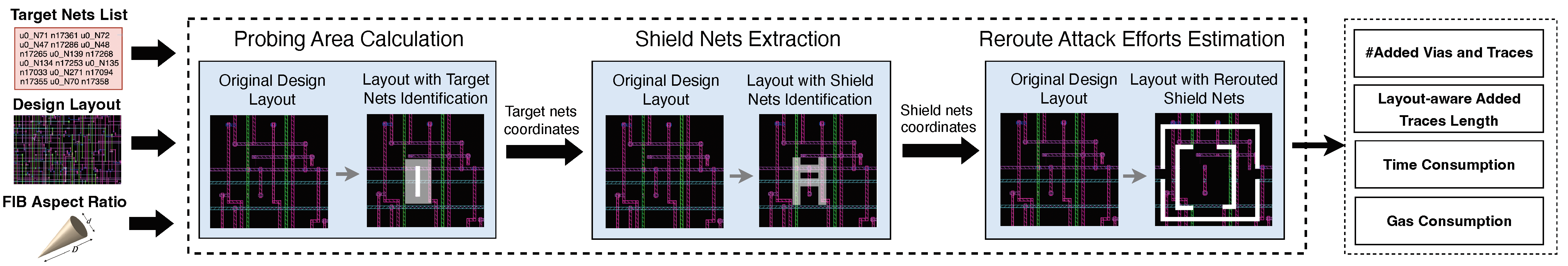
3. Detour-RS Framework

In this section, we will first give an overview of our Detour-RS framework, which aims to evaluate the reroute attack vulnerabilities of target physical designs in a layout-aware manner. Next, we will detail each step, i.e., probing area calculation, shield and other obscuring nets’ extraction, and hybrid-optimization (HO)-based reroute attack effort estimation.

3.1. Overview

The objective of Detour-RS is to establish a layout-aware assessment framework that can comprehensively and accurately assess the vulnerabilities of security-critical nets against FIB reroute attacks by taking floorplanning, cell placement, and routing of the target implementation into consideration. The workflow of the Detour-RS is illustrated in Figure 6, where the solution takes two main inputs, i.e., the design GDSII layout (.gds) and a designated list of target nets, which may serve as the interest of adversaries, e.g., transferring security assets. In addition to these two main inputs, users are supposed to provide inputs such as the FIB aspect ratio (see Section 2.1), which is critical since it aligns the analysis with the capabilities of potential adversaries. The Detour-RS framework consists of three stages: i.e., probing area calculation, shield and other obscuring nets’ extraction, and reroute attack efforts’ estimation. These stages collectively produce assessment results quantifying how difficult reroute attacks would be on the target implementation. The results include metrics such as the number of added vias, the number of added traces, the length of added traces with layout awareness, and time and gas consumption.
The general flow of Detour-RS is as follows. The framework starts with extracting essential layout information, specifically pinpointing the positions of metal wires associated with target nets. This information is then used to calculate the exposed area (more details will be presented in Section 2.4), which helps identify vulnerabilities based on the user-defined FIB aspect ratio. Next, Detour-RS identifies a set of protected shield nets corresponding to each target net. Subsequently, Detour-RS focuses on the analysis of shield nets residing within the probing area. To achieve this, a combination of nonlinear and linear programming techniques is employed to determine the precise locations where adversaries may introduce circuit edits on each shield net for effective reroute attacks. These calculated edits collectively represent the overall reroute attack efforts required.

3.2. Probing Area Calculation

The probing area calculation phase takes inputs from the design layout, a list of target nets, and the specified FIB aspect ratio. This step will identify the wire instances corresponding to the target nets as potential victims of reroute attacks. Note that a target net typically corresponds to multiple metal wire instances (often referred to as shapes) in the layout design. These wires carry different labels and can be situated across various metal layers. For example, as one can see in Figure 7, a target net n8998 comprises three wire shapes, i.e., Path_15_18553 (horizontal), Path_15_18554 (vertical), and Path_15_18557 (horizontal). Initially, Detour-RS will determine the metal layer to which each target shape belongs. Subsequently, the framework conducts an assessment to estimate the exposed area projected onto the uppermost layer by using the parameter d f a r e d g e as detailed in Equation (1).
More specifically, to determine the exposed area associated with the target nets, Detour-RS performs an iterative process, examining each shape within the target nets. It then provides information regarding the dimensions of the exposed area and the ratio of this exposed area concerning the target net. Regarding the wires depicted in Figure 7, we can obtain information about the dimensions of the exposed area and its corresponding ratio as presented in Table 1. It is important to note that, in this context, Detour-RS prioritizes the wire with the largest exposed area over the ratio, as it is conceivable that a metal wire with a higher exposed ratio might actually have a relatively smaller exposed area. Consequently, the region exhibiting the greatest level of exposure will be identified as the optimal candidate for the reroute attack adversaries and call for additional protection from designer perspectives (see the exposed/protected area as colored in Figure 7).
To give readers greater intuition regarding the exposed area, we also present examples of two AES physical implementations in Figure 8, where milling exclusion area is represented in blue, the exposed area in red, and the target nets’ area in yellow. It is visually obvious that the AES design in Figure 8a exhibits significantly greater vulnerabilities compared to the one in Figure 8b according to the exposed area (red) of the wires after Detour-RS analysis. Under the hood, the vulnerability of the first design (Figure 8a) can be quantified in the proportion of its exposed area, which stands at 62.28% in contrast to the 8.77% in the other design (Figure 8b), which indicates a larger exploitable space for probing intrusions.

3.3. Shield and Other Obscuring Nets’ Extraction

Metal wires that obstruct an attacker’s access to the target net can be categorized into two groups, i.e., shield nets and other obscuring nets. Shield nets refer to the internal nets that are strategically deployed to protect the target net from probing intrusions. The process of identifying and constructing these shield nets has been detailed in Section 2.2. The second category other obscuring nets is the inherent design wires, which are routed on the layers above the target net layers. These wires can also serve to obscure and complicate an attacker’s path to the target, adding an extra layer of security besides the shield nets.
We follow the flow in Algorithm 1 to extract shield nets for each target net. Specifically, we need to first calculate the exposed area for target nets as detailed in Section 3.2. The inputs to this stage are the physical design layout Layout, coordinates of target wires Tar, the user-specified FIB aspect ratio R F I B , and the technology library parameters T e c h p a r a such as the wire width, the distance between each metal layer, and the process variation margin; as shown in Equation (1), a value of d f a r e d g e can be obtained, which determines the size of the milling exclusion area (MEA), as shown in Figure 5. Then, the EA can be acquired by obtaining the complement area on the target wire area projected onto the topmost metal layer. Finally, all the obscuring nets and locations in the upper metal layer that cross the EA of the current target wire will be reported, including their coordinates and metal layers in the design layout.
Regarding the details of the shield net and other obscuring nets’ extraction, in the case of each target net, the wire with the largest exposed area is selected, and its probing area is subsequently determined at the topmost metal layer. It is within this area that the necessary vias and traces for rerouting all obstructing nets will be incorporated when executing a reroute attack. This proactive identification of the probing area on the topmost metal layer ensures that, in the event of a reroute attack, the essential rerouting components will be strategically positioned for optimal effectiveness. The physical design tool operates with a set of inputs, including the physical design layout, FIB aspect ratio, and technology-related data. Its initial task is to pinpoint and quantify the exposed area associated with a target wire. This involves identifying the region of the wire’s surface that is susceptible to probing. Then, the tool proceeds to compile a comprehensive list of all the obscuring nets that intersect or overlap with the current probing area. These obscuring nets are those wires and components that obstruct or shield the target wire under consideration.
Algorithm 1: Shield nets’ extraction.
Input: Layout—physical design layout
Input: Tar—coordinates of target wires
Input: R F I B —FIB aspect ratio
Input: T e c h p a r a —technology parameters
Output: d f a r e d g e of the target wire
Output: MEA, EA—MEA and EA of the target wire
Output: C o o r s h i e l d —coordinates of the shield nets
Output: L a y e r s h i e l d —metal layer of the shield nets
1Load the physical design layout Layout
2Input RFIB, Techpara, and Tar, and identify the dfaredge
3Apply the d f a r e d g e of the target wire, and identify its MEA
4 EA = { A r e a | A r e a T a r a n d A r e a M E A }
5{ C o o r s h i e l d , L a y e r s h i e l d } = g e t o b j e c t s b y l o c a t i o n i n t e r s e c t EA
Figure 9 gives more intuition of the entire procedure. After the identification of the target net exposed area (red rectangle in the lower layer), blue and green shield nets can be recognized to cross with the pink probing area from different upper metal layers in Figure 9a. The extracted shield nets will then be used to estimate reroute efforts, i.e., the black vias and purple lines to be added by FIB to access the assets without breaking the original design/shield net connectivity (see Figure 9).

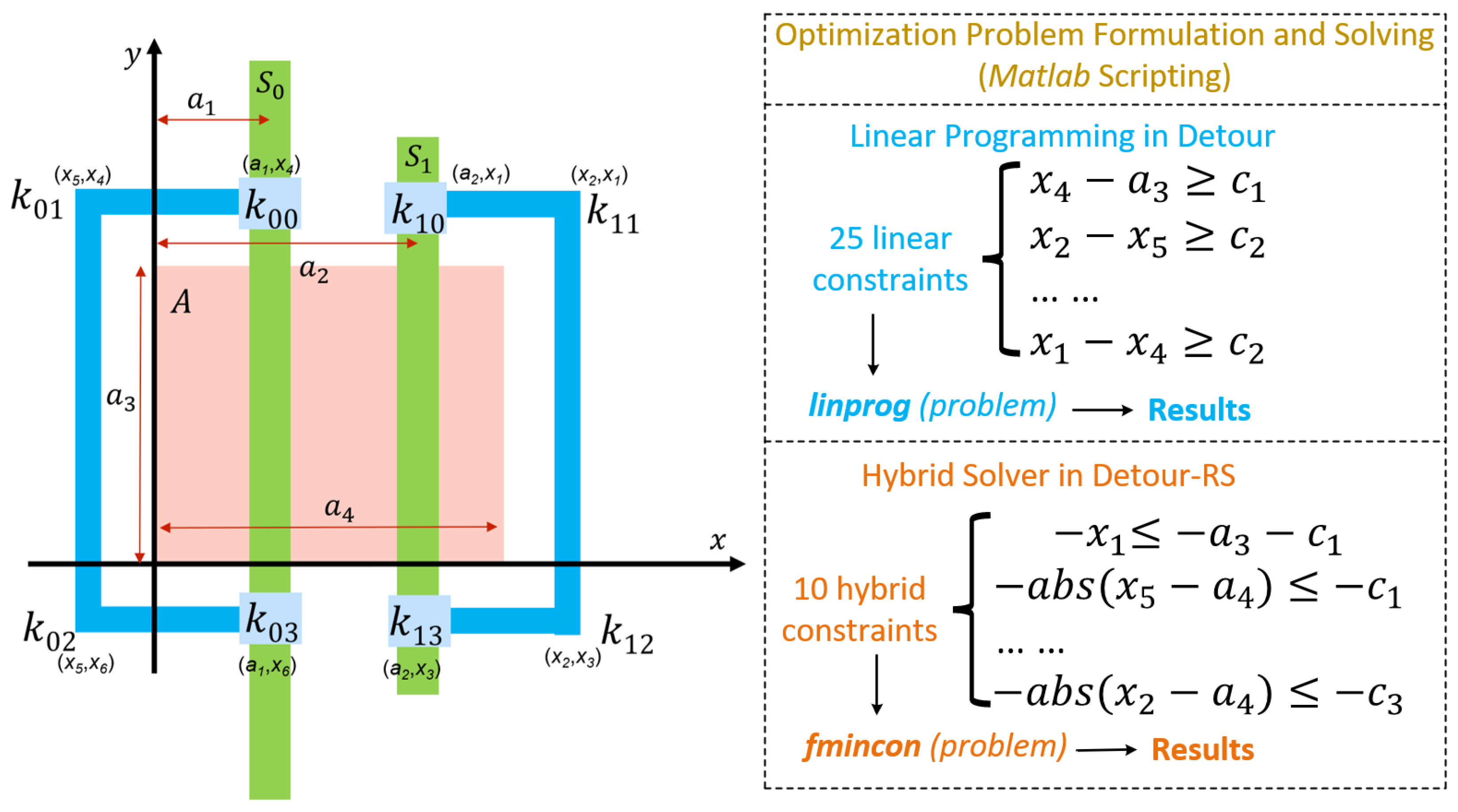
3.4. LP-Based Reroute Attack Effort Estimation

To evaluate the design susceptibility to reroute attacks, we introduce the following three metrics to reflect the required reroute attack efforts:
(i) Layout-aware added trace length: This metric refers to the length of traces added by the reroute adversaries, which are necessary for a successful reroute attack. We take the specified design information into account to enable layout-aware calculation. Generally, for each target wire, we will first identify its exposed area as detailed in Section 3.2 and then determine the location of vias that result in the minimum length of added trace to perform the reroute attack by following the programming strategy to be articulated in this section (Algorithm 2). The layout-aware added trace length metric will be calculated as the sum of the length of all the added traces.
Algorithm 2: Hybrid optimization in estimating reroute paths.
Cryptography 08 00013 i001
(ii) Time consumption: This refers to the amount of time spent by the FIB to perform the milling.
In FIB systems, a combination of gases is employed to generate and control the ion beam, with specific gases for sputtering and milling actions. Accurate measurement and analysis of gas and time consumption provide insights into the operational overhead associated with such attacks, helping to evaluate their feasibility and cost-effectiveness. It is defined as
T i m e C o n s u m p t i o n = 1 V R × I ,
where the sputtering rate, represented by R, characterizes the speed at which material is removed or sputtered from the target’s surface, while the sputtered volume, V, indicates the amount of material removed during the attack. The beam current, I, represents the flow of ions in the ion beam, impacting the rate at which material is sputtered. Note that the gas consumption metric serves as a vital parameter to gauge the efficiency and resource utilization during the attack process. As a critical metric, gas consumption plays a role in characterizing the resource demands and environmental implications of FIB probing attacks, which is essential for understanding their practicality and assessing the operational cost of FIB-based invasive attacks.
(iii) Gas consumption:
G a s C o n s u m p t i o n = T T C × P E ,
where time consumption, TC, refers to the amount of time spent by the FIB to perform the milling. T refers to the target assets volume. Process efficiency, PE, measures how effectively the gas is utilized. Not all of the injected gas might end up being used for deposition due to various factors like gas diffusion, reactivity, and chamber conditions. It is usually expressed as a percentage and indicates how much of the gas used contributes to the FIB milling. A lower process efficiency means that more gas is wasted in the process, resulting in higher gas consumption.
We describe our reroute attack estimation methodology, based on the combination of linear and nonlinear programming methods, in detail in Algorithm 2.

3.4.1. Independent Scenarios

The algorithm’s operation relies on five primary inputs: the physical design layout (Layout), the technology library constraints for hybrid optimization (C), a set of target nets Tar = { T a r 1 , T a r 2 , …, T a r M } that carry security assets, where M refers to the number of target nets, including the set of exploitable probing areas A p r o b = { A p r o b 1 , A p r o b 2 , …, A p r o b M } for each target net, and sets of obscuring or shield nets associated with each target net within the Tar set. Utilizing Algorithm 2 and the hybrid optimization (HO) engine, we can effectively determine the minimum total length (L) required for feasible reroute attacks and establish the precise placement of vertices for each added reroute trace. Algorithm 2 follows this general flow:
  • Stage 1: Initialization and processing (lines 1–9):
Algorithm 2 initiates its operation by extracting the placement and routing information from Layout. Subsequently, it centers its attention on the M target nets that carry security assets, which are the crucial points for probing attempts. To facilitate this process, the algorithm establishes the variable L i ¯ and the constraint set C i , which are the variables that are employed to track the added trace length and define the optimization constraints, respectively. We retrieve the ith target net, denoted as T a r i , from the set Tar. Along with it, we can gather essential information, including the probing area A p r o b i and the relevant shield nets contained in Shield i .
  • Stage 2: Added trace length formulation and constraints (lines 7–21):
Within the collection of shield nets Shield i , each shield net, S h i e l d i , j , contains several vertices required for the reroute attack added traces, denoted as Vertices i , j . As depicted in Figure 9c, each reroute path is determined by the positions of four vertices. Consequently, the length of the added trace, L i , j , can be computed as the sum of the distances between these vertices: L i , j = [ d ( V 1 , V 2 ) + d ( V 2 , V 3 ) + d ( V 3 , V 4 ) ] i , j . It is worth noting that L i , j is a linear function that will be addressed using the hybrid optimization programming method, subject to specific constraints. These constraints, denoted as C 1 and C 2 and detailed in Table 2, are stored within the set C to be utilized in the subsequent hybrid optimization process. In detail, C 1 defines the minimum distance required between consecutive reroute vertices, while C 2 specifies the minimum distance between any reroute vertex and the closest boundary of the corresponding probing area A p r o b i . To establish these constraints for the hybrid optimization in the subsequent phase, we iterate through each vertex V i , j , k with respect to the shield nets S h i e l d i , j .
  • Stage 3: Hybrid optimization for reroute attack efforts’ estimation (lines 22, 29, 30):
Based on the linear function and constraints, we can express the linear programming problem in the form of Equation (4) as shown in line 22.
{ Vertices i , L i } M i n ( L i ¯ ) s u b j e c t t o C i .
Below, the optimization constraints included within our framework are elaborated below, denoted as C i . It is important to note that the minimum distance between different segments of the metal wire can vary depending on the technology libraries used. Table 2 provides a comprehensive list of notations and their corresponding definitions:
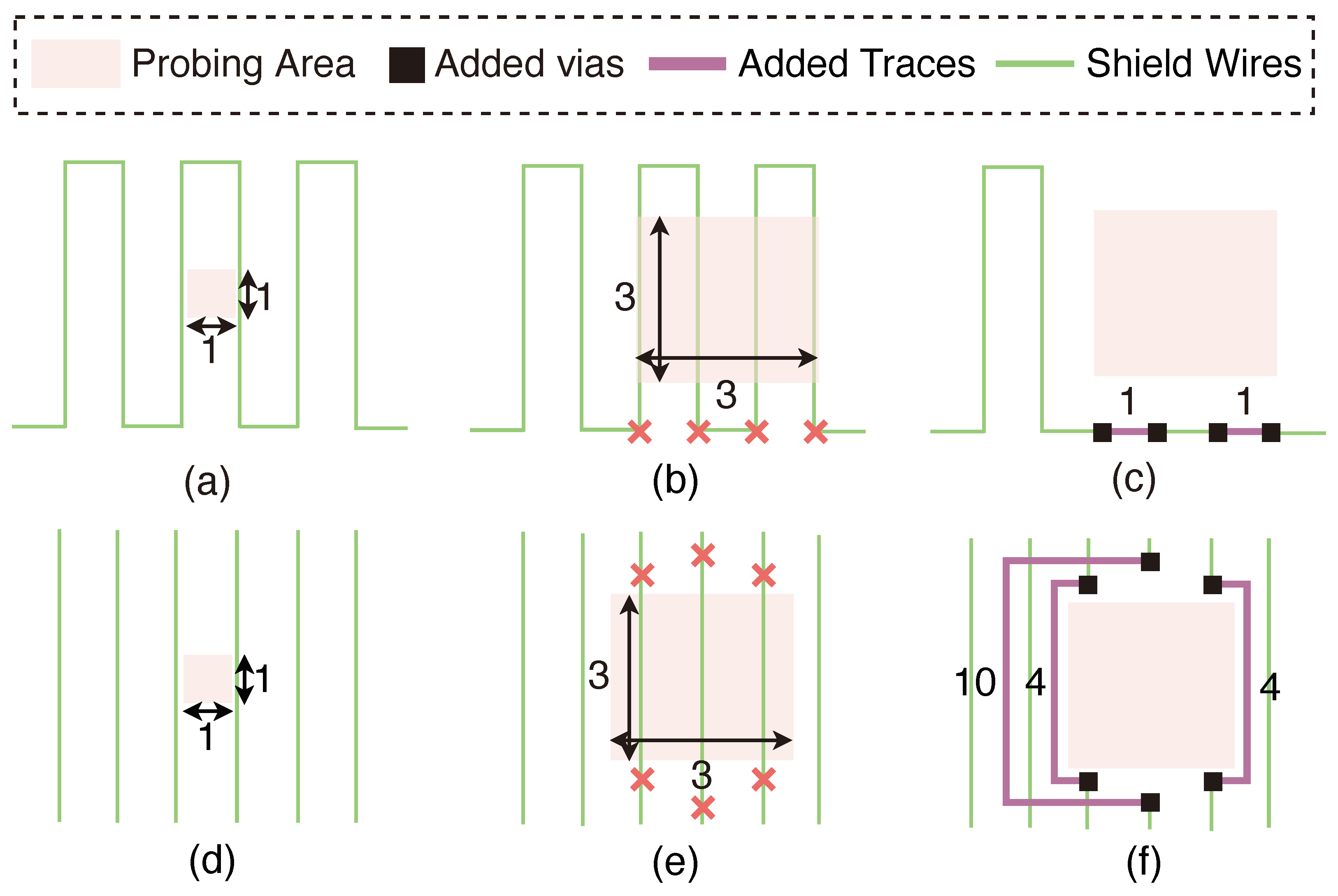
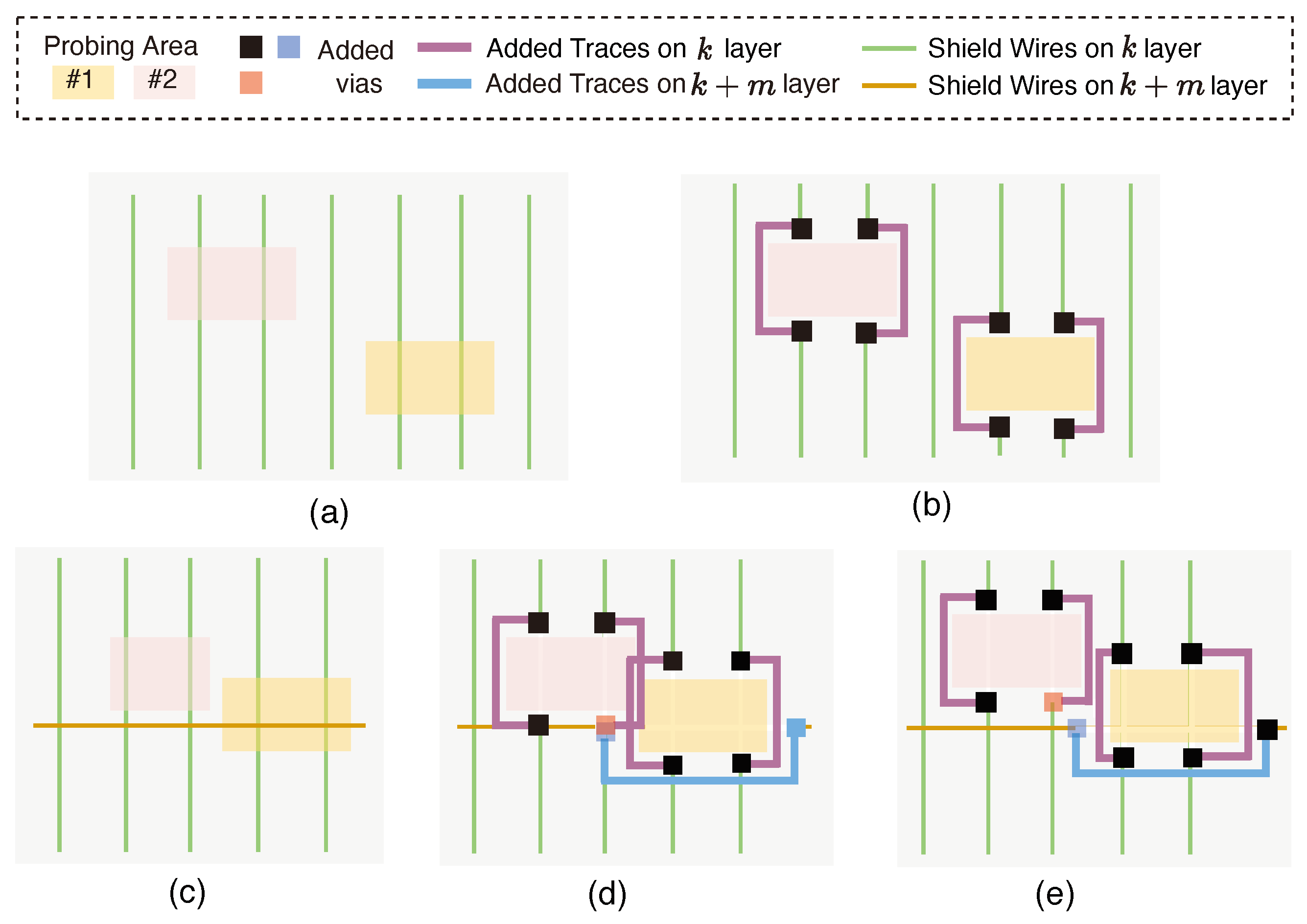
  • The first set of constraints enforces that a certain distance between each segment of the added traces in the layout must be maintained to ensure the signals extracted from the target nets to be reliable, which are expressed as
    D V T > d V T , m i n
    D V V > d V V , m i n
    D T T > d T T , m i n .
    Here, we include the distance requirements between vias, between vias and metal wires, and between wires, to avoid consequences such as the short of the signals.
  • The next constraint enforces that no traces cross in the same layer and is incorporated for the same reason as the first constraint. It can be stated as
    T r a c e i T r a c e j = .
  • To avoid affecting the normal signal transmission of shield wires, a minimum space will be reserved between traces and the probing area of the target net, expressed as
    D T P > d T P , m i n .
Subsequently, our hybrid optimization approach will automatically determine the most favorable scenario in which the added trace length for reroute attacks can be minimized adhering to the constraint set C i . Beyond just identifying the numerical value of L i , this methodology also provides insights into the precise positions of the Vertices of reroute traces for further analysis. Gathering the individual L i values and the corresponding Vertices for every target net T a r i , we can derive the comprehensive layout-aware results through the utilization of Algorithm 2, denoted as L and Vertices.

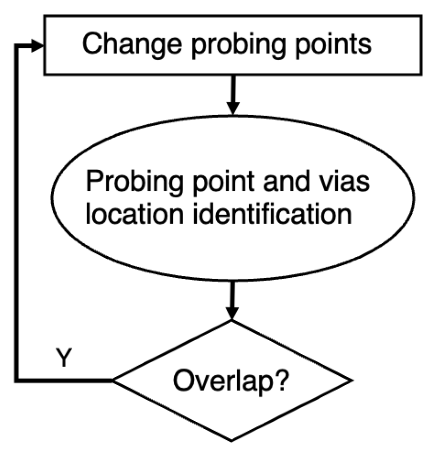
3.4.2. Dependent Scenarios

It is assumed in Section 3.4.1 that each target net can be probed independently of all others. Nevertheless, in practice, attackers typically have a finite number of FIB probe tips, whereas there may be hundreds of target nets, and thus, attackers cannot simultaneously probe all the target nets. Therefore, it is possible that the circuit edit sites on the topmost layer for different shield nets will overlap if attackers probe one target net after another. To address this dependence, the positions for overlapping reroute attack edits may require adjustment to prevent interference. Figure 10a,b depicts the scenario when edits do not overlap; as a result, the reroute effort estimate given under the independent flow is acceptable, and there is no need to move the probing area. A scenario where overlaps may occur is illustrated in Figure 10c. Consequently, the estimation of reroute attack efforts in the independent case is overly optimistic. In real-world scenarios, this would not be feasible due to the overlap between the probing areas and FIB edits, as demonstrated in Figure 10d. The dependent approach for estimating reroute attack efforts rectifies this situation by adjusting the position of probing area #1 to prevent overlap. This approach is more precise and could result in a higher reroute attack estimate if the new position of probing area #1 is less ideal, meaning it contains more obstructing nets compared to the previous position.
During the identification of via locations for various shield nets, if it is observed that a shielding net’s circuit edit location overlaps with the via location of another target net, it would be necessary to reposition the shielding net’s circuit edit. To address this concern, a constraint is integrated into the assessment process, which is depicted in Figure 11 and is implemented in Algorithm 2 (lines 23–28). When we take into account the constraint that prohibits location conflicts of the vias, a scenario referred to as the dependent case, we begin by recording the coordinates of the vias. Then, as we identify the location of the current via, we will carefully examine whether it overlaps with any other vias. If, indeed, an overlap is detected, we will need to follow the process outlined in Figure 11. Specifically, we will move the position of the probing area for the current target until it no longer overlaps with the probing area of a previously edited target.

4. Experimental Results

In this section, we start by detailing our experimental setup including the experimental layout designs employed. Following this, we delve into an extensive discussion of the results obtained from reroute attack efforts. These results are presented separately, addressing both independent and dependent scenarios, leveraging the capabilities of the Detour-RS framework.

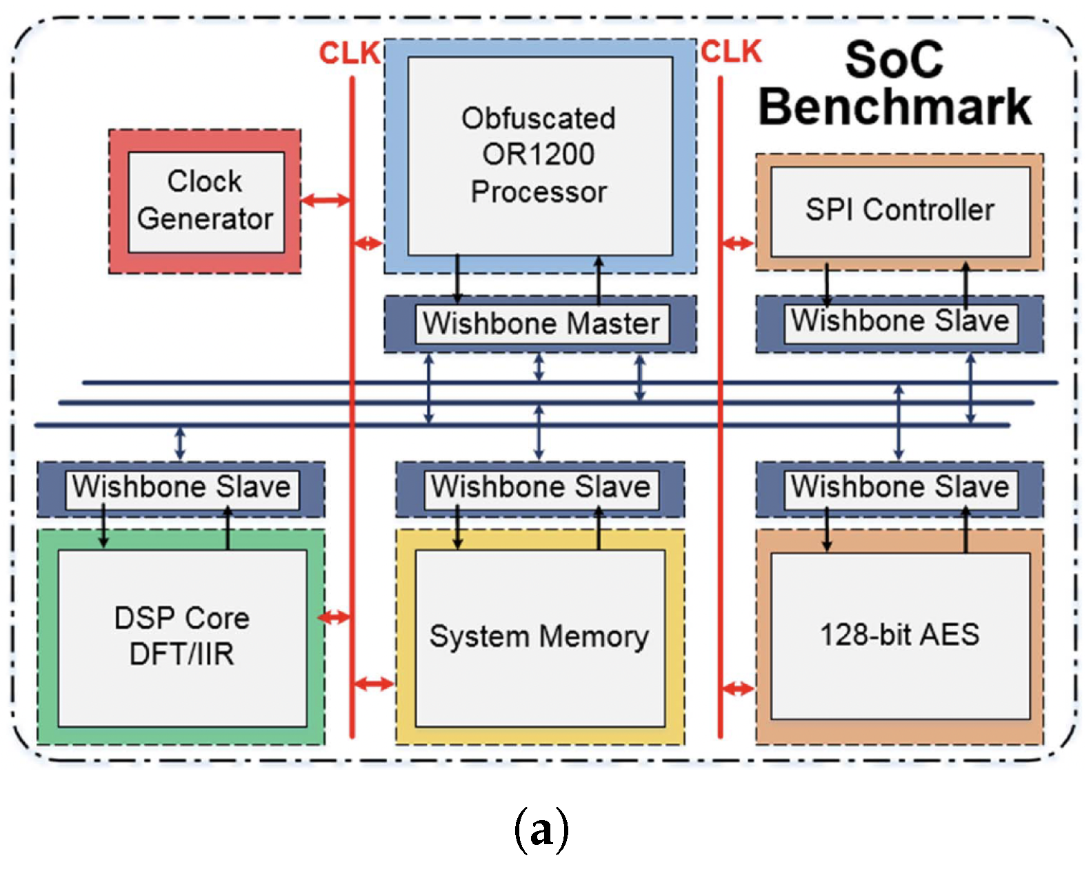
4.1. Experimental Setup

In this section, we leverage our Detour-RS approach to assess various design layouts in the context of reroute attacks. Our primary objective is to quantify how much effort adversaries have to spend for a successful probing attack. We consider different experimental configurations including the shield and asset nets, enabling comprehensive evaluation of the design resilience under varying circumstances. Besides, we conducted a comparative analysis between our layout-aware estimation results and those obtained through the state-of-the-art technique [14]. Furthermore, our evaluation covers the probing execution on each target net in both the dependent and independent scenarios, where the key difference between these two scenarios is whether the overlapping of the circuit edits is allowed or it needs to adhere to constraints preventing such overlaps.
For a fair comparison between our approach and the methodology presented in [14], we used the same benchmark implementation, i.e., the common evaluation platform (CEP) [33], a well-established SoC platform providing a common foundation for our evaluation. As illustrated in Figure 12a, the SoC design comprises several main components, including a core for AES encryption, a DSP core, an SPI controller, a data bus structure managed by an Arbiter, and a clock generator. We compiled the register-transfer level (RTL) implementation of the CEP benchmark to its physical layout using the Synopsys Design Compiler and Synopsys ICC2, with the SAED 32nm technology library. For consistency with the evaluation in [14], we selected an identical set of target nets. These target nets encompass critical elements, specifically the 128-bit encryption key nets of the AES module, the 32-bit data bus nets connecting the OpenRISC processor (OR1200) to the AES module, and the 64-bit obfuscation key nets within the OpenRISC processor, as depicted in Figure 12b.

4.2. Evaluation

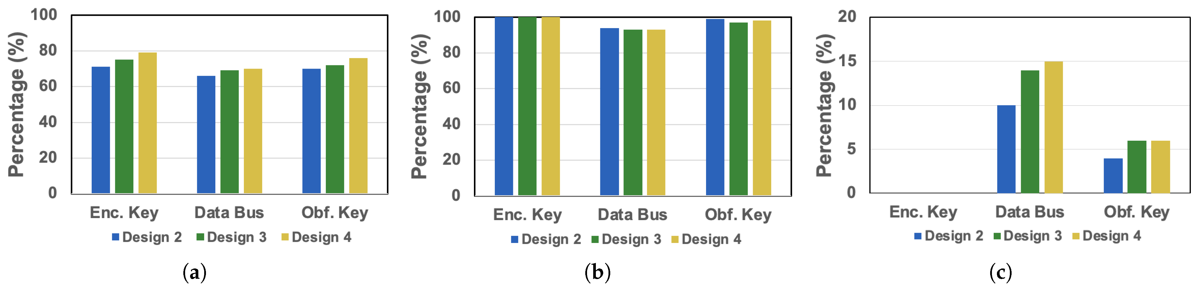
4.2.1. Independent Scenarios

We first present an independent evaluation of reroute attack vulnerabilities that focus on various probing targets, considering the possibility of overlapping circuit edits. This assessment quantifies reroute efforts using three metrics; in addition to the layout-aware added trace length as detailed in Section 3.4, we also utilized the number of added traces (shapes) and the number of added vias, which are intuitive to provide more insights.
As mentioned in Section 4.1, our analysis will cover different experimental configurations. Here, we introduce our four configurations of the target implementations (see Table 3) in this set of experiments as follows:
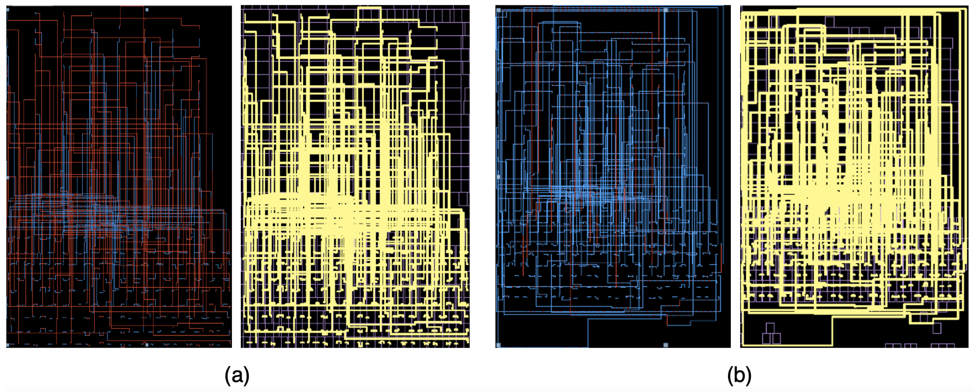
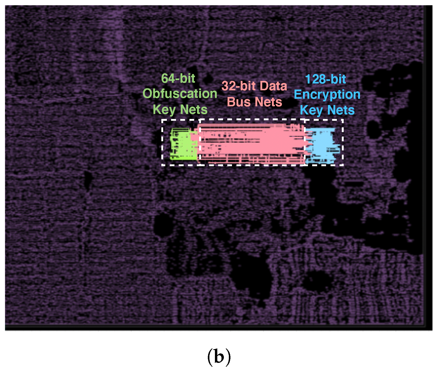
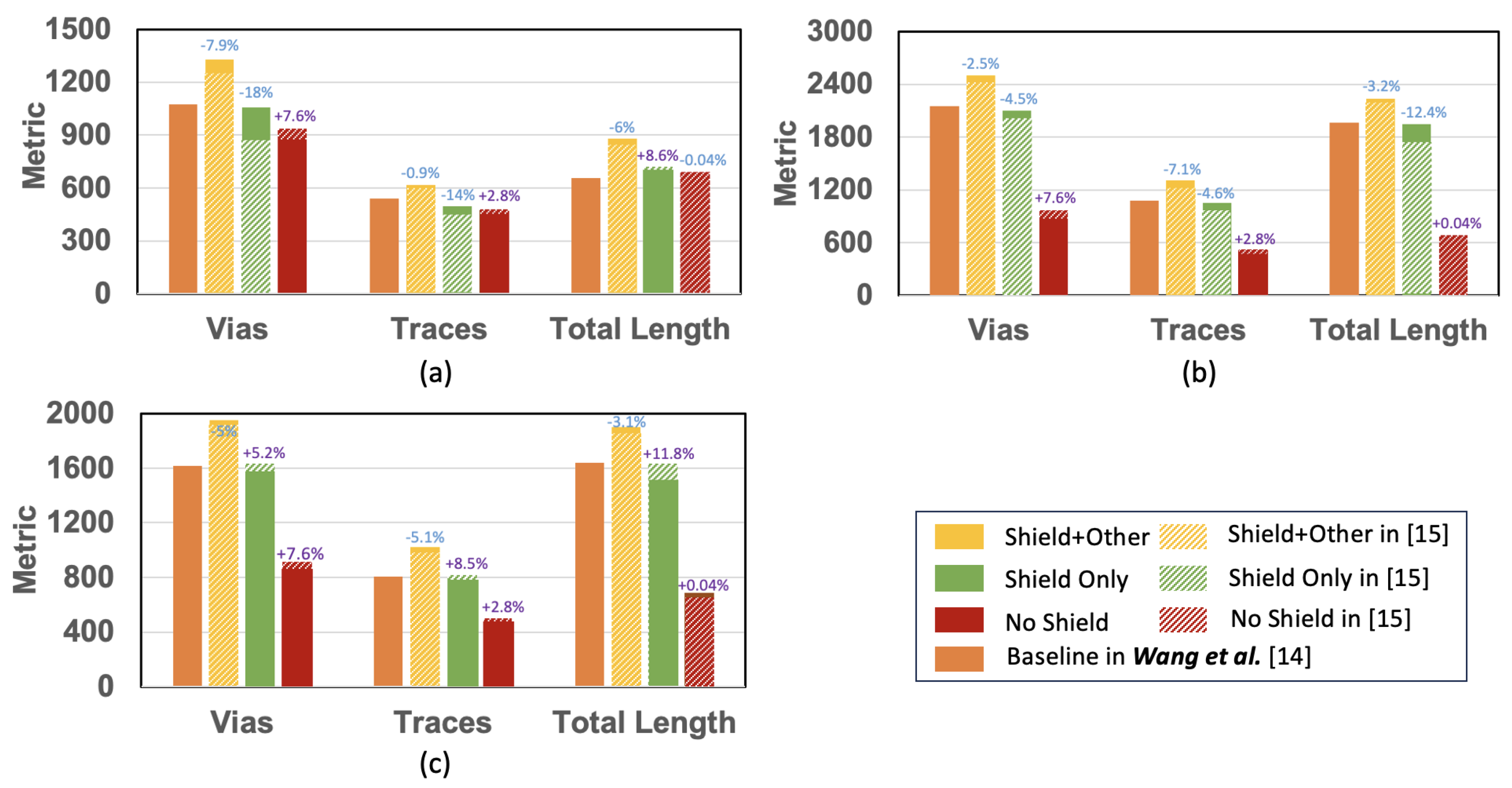
  • Design 1: the original CEP physical layout without any dedicated protection (shield nets) against probing or reroute attacks. Security resilience depends on non-shield obscuring nets.
  • Design 2: the CEP physical layout with a one-layer single shield at the M6 layer.
  • Design 3: the CEP physical layout with a two-layer orthogonal shield at the M6 and M7 layers.
  • Design 4: the CEP physical layout with a two-layer parallel shield at the M6 and M8 layers.
We performed a comprehensive reroute attack vulnerability assessment on these four designs using our Detour-RS solution and present the results in Table 4. First of all, we focus on our results at the bottom of Table 4, where three scenarios, no shield nets considered, only shield nets considered, and shield nets + other nets considered, were analyzed for metric calculation. More specifically, we first analyzed Design 1, i.e., without any dedicated protection, as a start. As mentioned, we have three groups of target nets, i.e., the AES encryption key nets, data bus nets, and obfuscation key nets (the AES-sensitive signals will be discussed in Section 5.3). Besides, we also targeted Designs 2/3/4 with different shield structures by considering the protection provided by only shield nets and shield nets + other nets. Moreover, we also included the results from Wang et al. [14] and our previous Detour framework, i.e., Gao et al. [15], for comparison. We would like to highlight that Wang et al.’s results [14], serving as the baseline of both Detour and Detour-RS results, are based on assumptive theoretic derivation without any awareness of target layout information.
We can observe from Table 4 that the baseline design layout without any shield structures (Design 1) demands the smallest quantity of reroute attack efforts, rendering it the least secure option among the design layouts examined. For example, rerouting all AES encryption key nets with our Detour-RS solution utilizing hybrid optimization algorithms necessitates only 380 added vias, 190 added traces, and 122 mm of additional trace length. However, when both shield nets and other functional nets are employed for protection (shield nets + other nets), the most effective safeguard appears with the deployment of a two-layer orthogonal shield at M6 + M7. In this scenario, the resources are required compared to the baseline, translating to 1232 added vias, 616 added traces, and 355 mm of added trace length. It is essential to acknowledge that inherent randomness during design placement and routing may introduce variations in resiliency. For instance, the total added trace length for the only shield nets case with a single-layer shield at M6 is slightly lower (1769 mm) than the baseline (1800 mm) for the data bus assets.
We also label the percentage for each value of Designs 2/3/4 ([14] did not cover Design 1) for both the Detour-RS and Detour results under all scenarios compared to their corresponding counterparts in the baseline results in Table 4 for clearer visualization. One can also observe that the estimations in the baseline results [14] generally exceeded the estimations in the only shield nets scenarios, but fell short of the estimations in the shield nets + other nets scenarios provided by our Detour-RS framework. The fundamental reason is that [14] assumes the maximum number of shield nets that can always be accommodated in the layers above the target nets’ area, without accounting for practical constraints and potential routing congestion. Consequently, the attack cost is computed purely on theoretical analysis within an idealized context. However, in practice, for a thorough assessment, Detour-RS acknowledges that not all shield nets can be exclusively placed on their designated metal layers; some may need to be accommodated on other metal layers due to spatial limitations (e.g., congestion). In essence, our experimental results highlight that the assumptions made in [14] lack fairness and tend to provide overly optimistic estimates regarding the available shield nets on the specified layer, thus yielding inaccurate results. Detour-RS rectifies these inaccuracies by considering the placement and routing conditions, including congestion, at the layout level across the entire design. A more detailed comparison between Detour and Detour-RS can be found in Section 5.1.
Additionally, Figure 13 illustrates the extent of protection provided by shield nets alone, presented as percentages for various design configurations. Remarkably, these figures consistently surpass 70%, with some reaching nearly 90%. This aligns with the results shown in Figure 13a, which highlights the proportion of shield nets in relation to all covering nets, indicating that almost 70% of the protective coverage is attributed to shield nets. Figure 13b offers insights into the distribution of target nets across different layers, demonstrating that they are effectively confined below the shield nets. Nearly 100% of target nets are routed and situated in their designated metal layers. In Figure 13c, we observe the portion of assets routed above the shield, revealing that a minimum of 85% of the targets are comprehensively safeguarded beneath the shield nets layer. It is noteworthy that, irrespective of the design’s shield structure, all encryption key nets are consistently routed beneath the shield.

4.2.2. Dependent Scenarios

We also conducted experiments to demonstrate the effectiveness of our Detour-RS solution in addressing dependent scenarios. In Figure 14a, Detour-RS’s visual results depict the reroute attack involving two probing areas (highlighted in grey) within the design layout. It is evident that these probing areas intersect, necessitating a reroute path on the green obscuring net for probing area #1 and on the blue obscuring net for probing area #2. This results in added trace lengths of 1.674 μm and 1.872 μm for the #1 and #2 probing areas, respectively. However, when considering the dependent scenario, our framework adjusts the probing area location to prevent conflicts in circuit edit positions, as illustrated in Figure 14d. In this case, the added trace lengths are 1.674 μm for the #1 and 3.160 μm for the #2 probing area, demonstrating the impact of rerouting to accommodate the dependencies between the probing areas.
Furthermore, we conducted an analysis of the iteration count to ensure that the circuit edit locations did not overlap. As the number of iterations increased, the reroute attack efforts for all designs also escalated, because, on the one hand, the process of re-identifying circuit edit locations became more time consuming. Moreover, relocated circuit edits led to longer traces being added, thereby increasing the overall attack cost. The iterations were systematically calculated ranging from 0 to 5. In Figure 15, we illustrate the distribution of the required number of iterations. It is apparent that the majority of cases needed just one or two iterations to determine the via locations, while a small fraction (less than 10%) required more than four iterations. Furthermore, we collected data on the total length of added traces after completing all the iterations. In some cases, orthogonal and parallel two-layer shield structures (Design 2 and 3) resulted in nearly a 50% increase in costs compared to the single-layer shielded design (Design 1). In addition, Table 5 provides a comparison of time consumption between the linear and hybrid optimization algorithms for various target asset categories in both the independent and dependent scenarios. It can be observed that it takes more time in the dependent case than in the independent case, which results in nearly three-times the time in some cases. In addition, the addition of the nonlinear algorithm leads to at most a 10% increase in time cost.

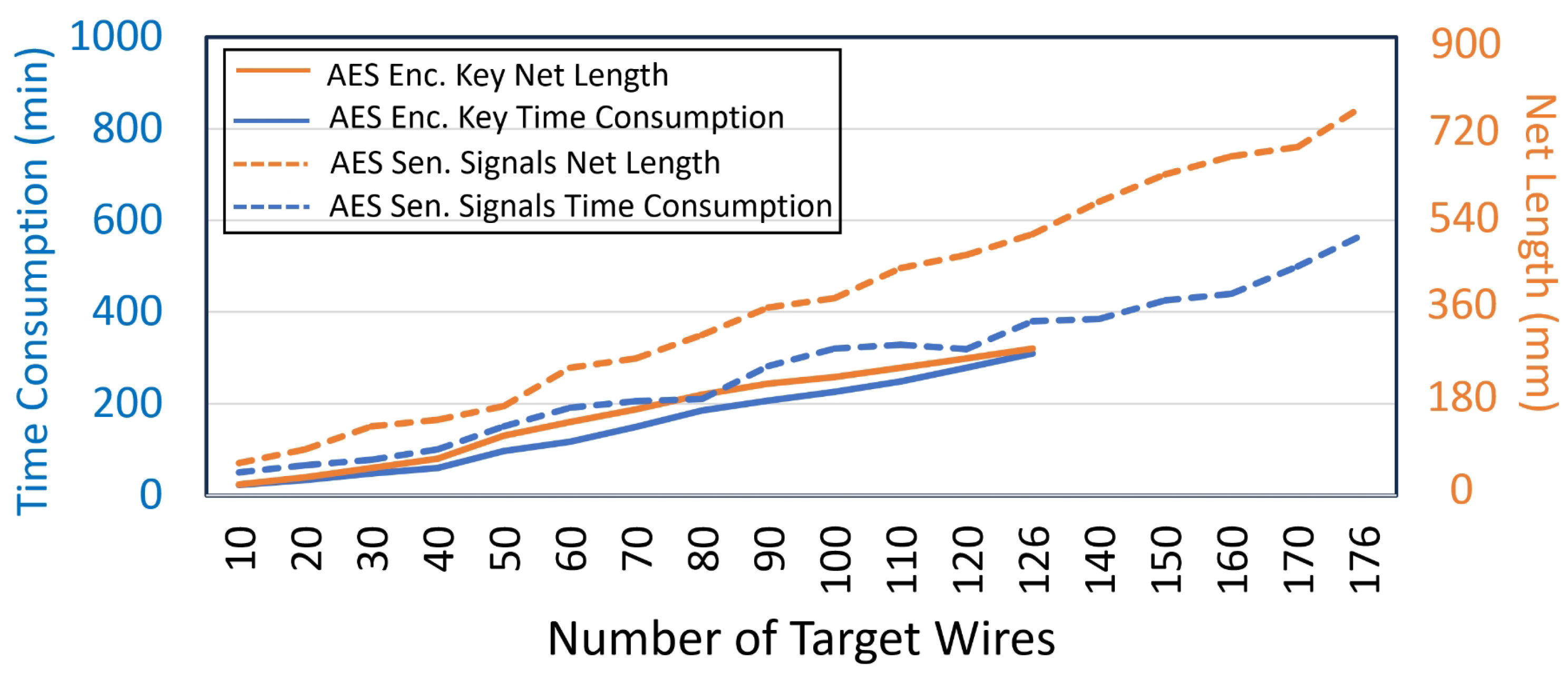
4.2.3. Time and Gas Consumption

It is assumed that the gas injection system nozzle will release Ga+ gas, whose atoms can be deposited within the milling cavity, establishing a conductive pathway as electrical probe contacts, and its typical sputter rate is 0.2 μm3/nC. In addition, the beam current is assumed to be 100 nA, and the process efficiency follows the normal distribution with the confidence interval between 0 and 0.9 under the 3-σ rule. We conducted a Monte Carlo simulation with 1000 randomly chosen process efficiency samples. Table 6 shows the time and gas consumption for each target asset category and the average results for each via during the FIB probing attack, where the units are seconds and microCoulomb for time and gas consumption, respectively. The calculation was conducted for Design 3, considering both the shield nets and other nets. It can be observed that time and gas consumption rise with the number of target nets, where the data bus takes the most resources.

5. Discussion

In this section, we will clarify some important concerns regarding our framework. Specifically, we will first compare Detour-RS with our Detour framework [15] in detail by presenting a case study. Next, we further discuss the advantages and disadvantages of our metrics and other possible ones. Finally, we present more experimental results to demonstrate the scalability of the Detour-RS framework.

5.1. Hybrid Model in Detour-RS vs. Linear Programming in Detour [15]

To give an intuitive understanding of the methodology difference between Detour and Detour-RS, we present the following case study, where a probing area A (in pink) is originally protected by two shield nets S 0 and S 1 (in green). Adversaries aim to utilize FIB capabilities to edit the shield nets as rerouted paths (in blue), exposing the probing area, as depicted in the figure above. To reroute the path like S 0 , two vias k 00 and k 03 need to be created at first to determine the ends of the rerouted path. The vias are connected to the highest metal layer such that adversaries can gain maximum rerouting flexibility. As such, a rerouted path k 00 k 01 k 02 k 03 of S 0 can be established to provide attackers with more space for micro-probing intrusions.
Adversaries are expected to follow formal rules for successful reroute attacks such as the following: (i) The vias (in light blue) cannot hang over the probing area A, otherwise the rerouted shield nets would be still cut off by intrusion, and detected by users. (ii) The rerouted paths should be kept away from the edges of the probing area A at least a minimal distance c 1 . (iii) The rerouted paths cannot cross each other to avoid short circuits. As one can see, what is in Figure 16 is a relatively straightforward example with only two shield nets. However, analyzing the constrained problem with only linear programming (i.e., our conference Detour version) can be complicated given the number of required constraints. The example constraints in this case study include, but are not limited to (i) x 4 a 3 c 1 , x 4 c 1 , x 1 a 3 c 1 , x 3 c 1 , (ii) x 5 c 3 , x 6 c 3 , x 2 a 4 c 3 , x 3 c 3 , and (iii) x 2 x 5 c 2 , x 1 x 4 c 2 , x 4 x 6 c 2 , x 2 x 5 c 2 , corresponding to rules (i), (ii), and (iii), respectively. In fact, the total number of this single case study can be up to 25, which is very cumbersome and error-prone in framework implementation. In contrast, our new Detour-RS framework employs a general hybrid solver allowing for direct formulations of the objective function and associated constraints as follows.
Target function: T = min abs(( a 1 x 5 )) × 2 + abs( x 4 x 6 ) + abs(( a 1 x 2 )) × 2 + abs( x 1 x 3 ).
This is subject to the following (10 hybrid constraints):
  • x 1 a 3 c 1 ;
  • x 3 c 1 ;
  • x 4 c 1 ;
  • x 6 a 3 c 1 ;
  • a b s ( x 5 ) a b s ( x 5 a 4 ) a 4 ;
  • a b s ( x 5 ) c 1 ;
  • a b s ( x 5 a 4 ) c 1 ;
  • a b s ( x 2 ) a b s ( x 2 a 4 ) a 4 ;
  • a b s ( x 2 ) c 1 ;
  • a b s ( x 2 a 4 ) c 1 .
Note that, for advanced scenarios, where three or more shield nets need to be considered, the formulating simplification could be even more notable. Some of the underlying simplifications might stem from the fact that we can compress multiple linear constraints into a single one with a representation of absolute values. Although those simplifications cannot essentially accelerate the problem’s analysis, our Detour-RS framework (gradient-based nonlinear solver) can still benefit from them since a smaller number of constraints indicate more conciseness and less likelihood of errors especially given some existing linear programming solvers (e.g., linprog in Matlab) do not accept representations with absolute value arguments.
In addition to the improved simplicity and accuracy, we also identified some cases that are more suitable to be modeled as a nonlinear optimization problem, which can only be handled by our new hybrid Detour-RS. More specifically, the objective function may have to target the probing area instead of the added traces’ length in some special cases, which results in a nonlinear optimization problem (because probing area calculation is a nonlinear function), as depicted in Figure 17. We illustrate an example scenario, as shown in Figure 17a above, where a target wire has two endpoints, p 1 and p 2 . Both p 1 and p 2 can be selected as probing points, while there are two shield nets s 1 and s 2 in place. Note that s 2 is at a higher metal layer compared to the one of s 1 . From an adversarial perspective, if one selected p 1 as the attack point, the probing area would be large because it should be considered for s 2 , which is at a higher metal layer, as seen in Figure 17b. In contrast, the attack point p 2 only needs to deal with the single shield net s 1 at a lower metal layer and, thus, obtain a smaller probing area, as illustrated in Figure 17c. Figure 17d,e depict how the rerouted paths can be constructed under different scenarios of the p 1 and p 2 attack points. We can clearly see that selecting p 1 for vulnerability assessment would be overestimating the required efforts of adversaries since p 2 is a more intelligent choice with a shorter added traces’ length during the attack. To deal with such a scenario, i.e., determining the appropriate attack points on a single target wire, our hybrid model has to be used to target the minimal probing area instead of the previous sum of added trace length in the objective function, ensuring a more reasonable and precise assessment result.
We also compared the results of our hybrid Detour-RS method with our previous linear programming-based Detour solution regarding the same benchmark layouts, where the theoretically estimated statistics from [14] were taken as the baseline. Figure 18 illustrates the comparison regarding Design 2 (single shield layer at M6), Design 3 (orthogonal two-layer shield at M6 and M7), and Design 4 (parallel two-layer shield at M6 and M8) in Figure 18a–c, respectively. We represent previous Detour results in dashed fill, while our Detour-RS results are in solid fill bars. The percentage of changes is labeled in the figure as well. One can see that there are some marginal differences between these two sets of results. The reason is that these results quantify the adversarial efforts; our Detour-RS is a more precise methodology compared to the Detour framework by reducing the likelihood of errors, covering all corner cases, and using a nonlinear solver to address special scenarios, as discussed above. In other words, the results are supposed to be more calibrated and accurate instead of simply becoming asymptotically larger or smaller. We can see some of the statistics like the added traces’ length of Design 4 considering shield nets only, i.e., the solid green bar in Figure 18c is increased. The root cause can be that Detour-RS fixed the missing corner cases or constraints in Detour and found a larger required added trace length, etc. As for the reduced statistics such as the added traces’ length of Design 4 considering shield nets and other nets, i.e., the solid yellow bar in Figure 18c, we identified where most of them come from. We addressed the probing point optimization issues by using our hybrid solver and, thus, determined the minimal adversarial efforts.

5.2. Discussion of Metrics

In our Detour-RS metric, we mainly utilized two different metrics, i.e., exposed area and layout-aware added traces’ length, for reroute attack vulnerability assessment for a given physical layout. Note that we also introduced two additional metrics, time and gas consumption, in this extension to reflect the adversarial efforts needed:
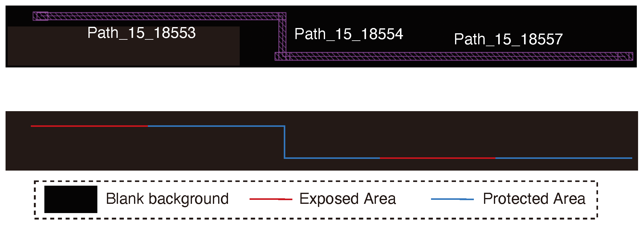
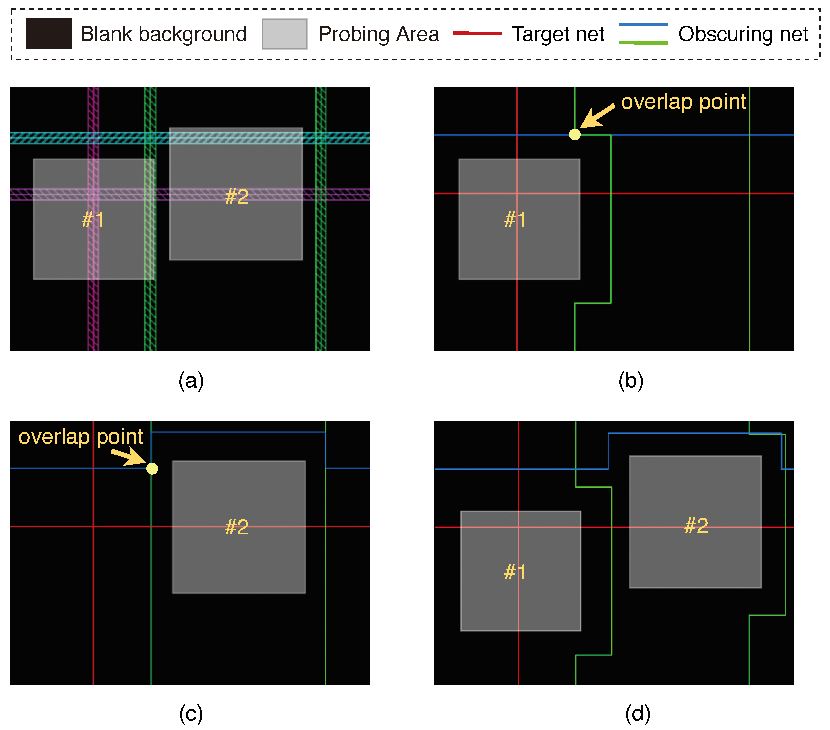
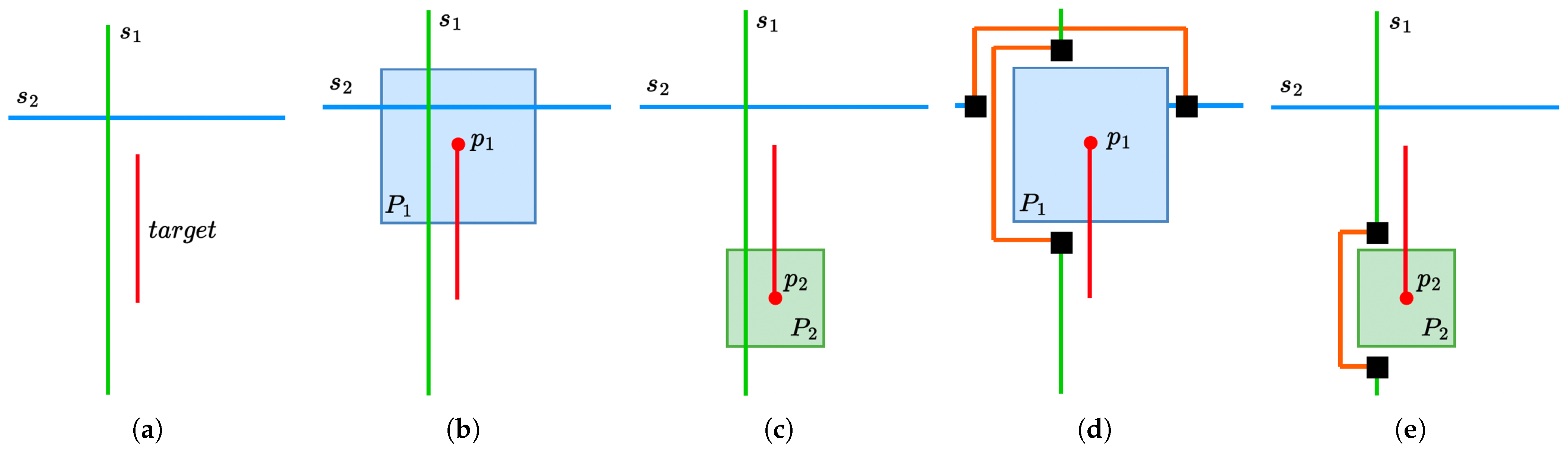
  • Exposed area: Exposed area refers to the exploitable space of a target wire for a micro-probing adversary. In other words, given the FIB configuration and precision, adversaries can place their probing points in the exposed area to access the target wire without cutting off any shield wires. Figure 5 illustrates the determination of the exposed area for the given target wire and covering metal wires, which are capable of providing protection to the milling exclusion area on the target wire. An adversary will tend to target the target wires with a larger exposed area since it implies easier reroute attacks. Therefore, in our framework, the exposed area is used to identify the target wire with the protected covering wires, where a reroute attack would be performed.
  • Layout-aware added traces’ length: This metric refers to the length of metal traces added by the reroute attack adversaries, which are necessary for a successful reroute attack. The greater the length of the layout-aware added traces, the higher the resource cost for attackers to perform a reroute attack is. Therefore, the metric itself and its variants (e.g., layout-aware added vias and layout-aware added traces) can effectively quantify the adversarial efforts of reroute attacks. For example, we comprehensively assess the vulnerabilities of reroute attacks in Table 4 given different scenarios, designs, and sets of target wires using the metric.
  • Time and gas consumption: When it comes to practical microprobing reroute attacks, the time and gas consumption of FIB are very important by reflecting the efficiency and cost of adversaries. The duration of the attack directly impacts its cost and feasibility. FIB systems are expensive to operate, with costs often billed by the hour. Therefore, an attack that takes less time is more cost-effective. Additionally, the availability of the FIB equipment might be limited, making time efficiency crucial. As for gas consumption, FIB systems use various gases for processes such as etching or deposition. The amount of gas consumed not only affects the operational cost, but also the feasibility of long operations. Efficient gas usage ensures that the attack can be sustained for the necessary duration without requiring excessive resources.
In addition to our metrics, other relevant ones have been seen in the literature. They can be useful in some cases for securing implementations while being limited or inappropriate in aligning with the goal of Detour-RS, i.e., reroute attack vulnerability assessment:
  • Added traces’ length [14]: This metric was proposed to evaluate reroute attack difficulty on different shield structures based on the calculation of added traces’ length. It quantifies the cost to mill a fixed-size area on a shielded design by reroute attacks for different shield structures. However, the added traces’ length metric is limited by its focus on fixed shield structures and theoretical cost calculations, which rely on the ideal positioning of shield nets within the design layout. In practice, routing conditions often fluctuate, resulting in suboptimal routing of shield nets due to factors such as congestion and restricted space within the protected area. In other words, the added traces’ length metric in [14] is more of a theoretical estimation instead of being aware of layout information. In contrast, the layout-aware added traces’ length metric in our Detour-RS framework provides a more accurate estimation by taking into account the specific design layout, rather than depending on the overly optimistic assumptions associated with fixed shield structures.
  • Target score [31]: This metric was used to quantify the likelihood of a net being targeted in a probing attack. The higher the target score is, the more sensitive information that the nets will carry. It can be used to identify the target nets and the shield nets that will provide protection. However, as the focus of our Detour-RS is vulnerability assessment, we do not need the target score metric at this stage, since it is designed for optimal countermeasure deployment.
  • Shield security [31]: This metric was proposed to identify the optimal metal layer where the shield and target nets will be routed, which will vary with different technology and FIB parameters. It will assist in providing the maximum protection to the target nets. Similar to the target score, shield security is also a countermeasure-oriented metric that could be utilized at the subsequent protection stage instead of the vulnerability assessment phase of our Detour-RS.

5.3. Scalability Evaluation of Detour-RS

Scalability is an important property of our Detour-RS solution and, thus, needs more inspection. To this end, we first inspected the scalability of our Detour-RS with respect to the number of target wires. We took the AES encryption key nets as an example; there are 128 corresponding wires in the benchmark layout. Our Detour-RS took 23 min to analyze the reroute vulnerabilities of 10 wires, while around 1 h for around 28 wires, as illustrated in Figure 19. A similar scalability (time vs. number of target wires) has been seen in the rest of the AES key encryption nets and data bus, as well as the obfuscation key nets. We can see that this is a nearly linear progress, which is good given the slow increase of time consumption for covering more target wires in a future complicated implementation. Based on our further analysis, we found that the time consumption was more linearly correlated with the total length of the target wires because the longer a target wire is, the more analysis is needed to evaluate its vulnerability under different given shield structures. The linear increase can be attributed to our fine-grained analysis of Detour-RS, making each of the sub-circuitries less dependent on each other.
Also, the scalability may vary with the net selection. In fact, we already selected three different groups of nets carrying sensitive security assets, i.e., AES encryption key nets, data bus, and obfuscation key nets. However, information leakage from data path signals or other intermediate nets within the AES coprocessor can be effectively exploitable. For example, round key values can be easily used to deduce the AES key as the key expansion procedure is reversible. S-box outputs can be utilized to deduce the round keys and further full keys considering a known plaintext/ciphertext. Therefore, we performed our Detour-RS analysis by covering a new set, called AES-sensitive signals, including the output wires of key expansion, S-box, and mix column modules, 176 in total for our benchmark implementation. We include the assessment results in the updated Table 4. Moreover, we found that analyzing these 176 AES sensitive signals took around 14 h for Detour-RS, suggesting the linear scalability of our Detour-RS tool as well (see Figure 19).

6. Conclusions and Future Work

This paper introduces an innovative layout and resource-aware framework for assessing reroute attacks, thereby enabling a comprehensive evaluation of potential vulnerabilities. Our approach incorporates a physical design and employs a synergy of linear and nonlinear programming techniques. This combination empowers the framework to autonomously identify optimal FIB probing locations, a critical determinant in defining the subsequent path of rerouted traces essential for executing the attack. Once the locations for circuit edits had been identified, we proceeded to quantify the cost associated with reroute attacks employing our layout-aware added traces metric and the time and gas consumption metric. Furthermore, we analyzed the reroute attack efforts within two distinct scenarios, i.e., the independent and dependent scenarios. Specifically, in the independent scenario, we allowed for the possibility of overlapping circuit edits across different target nets, while in the dependent scenario, such overlapping was strictly prohibited. The findings from our analysis showed that shielded designs consistently exhibited superior performance compared to their non-shielded counterparts. In particular, designs featuring a two-layer shield structure demonstrated a higher attack cost when compared to those with a single-layer shield. Especially, within the realm of two-layer shield layouts, those adopting an orthogonal configuration outperformed their parallel counterparts, signifying a distinct advantage. Furthermore, it is noteworthy that the dependent scenario exhibited a remarkable capability, resulting in an approximate 50% increase in attack cost compared to the independent case. Our paper mainly concentrated on the FIB milling while evaluating the time and gas consumption. In the future, we will expand our focus to include FIB deposition time, considering aspects like layer thickness and deposition rate. Furthermore, we will address the equipment navigation time, including the time taken for beam positioning and sample stage movement. These additions aim to offer a comprehensive understanding of the resources and time constraints associated with our approach. In addition, we envision expanding the Detour-RS framework to encompass a broader spectrum of FIB circuit edit attacks beyond probing. These extensions may include leveraging FIB to create opens and shorts within circuits, particularly with regard to security-critical nets involved in on-chip tamper detection and response mechanisms. Also, we will target more emerging device models such as large on-chip communication infrastructure [34] and 3D ICs [35].

Author Contributions

Conceptualization, methodology, software, validation, analysis, M.G. and D.F.; review and editing, L.K.B. and N.A. All authors have read and agreed to the published version of the manuscript.

Funding

This research was funded by NSF No. 2016624.

Data Availability Statement

The data is available from the corresponding author upon reasonable request.

Conflicts of Interest

The authors declare no conflicts of interest.

References

  1. Volya, D.; Zhang, T.; Alam, N.; Tehranipoor, M.; Mishra, P. Towards Secure Classical-Quantum Systems. In Proceedings of the 2023 IEEE International Symposium on Hardware Oriented Security and Trust (HOST), San Jose, CA, USA, 1–4 May 2023; IEEE: Piscataway, NJ, USA, 2023; pp. 283–292. [Google Scholar]
  2. Zhang, T.; Park, J.; Tehranipoor, M.; Farahmandi, F. PSC-TG: RTL power side-channel leakage assessment with test pattern generation. In Proceedings of the 2021 58th ACM/IEEE Design Automation Conference (DAC), San Francisco, CA, USA, 5–9 December 2021; IEEE: Piscataway, NJ, USA, 2021; pp. 709–714. [Google Scholar]
  3. Zhang, T.; Rahman, M.L.; Kamali, H.M.; Azar, K.Z.; Tehranipoor, M.; Farahmandi, F. FISHI: Fault Injection Detection in Secure Heterogeneous Integration via Power Noise Variation. In Proceedings of the 2023 IEEE 73rd Electronic Components and Technology Conference (ECTC), Orlando, FL, USA, 30 May–2 June 2023; IEEE: Piscataway, NJ, USA, 2023; pp. 2188–2195. [Google Scholar]
  4. Tajik, S.; Lohrke, H.; Seifert, J.P.; Boit, C. On the power of optical contactless probing: Attacking bitstream encryption of FPGAs. In Proceedings of the 2017 ACM SIGSAC Conference on Computer and Communications Security, Dallas, TX, USA, 30 October–3 November 2017; pp. 1661–1674. [Google Scholar]
  5. Zhang, T.; Tehranipoor, M.; Farahmandi, F. BitFREE: On Significant Speedup and Security Applications of FPGA Bitstream Format Reverse Engineering. In Proceedings of the 2023 IEEE European Test Symposium (ETS), Venezia, Italy, 22–26 May 2023; IEEE: Piscataway, NJ, USA, 2023; pp. 1–6. [Google Scholar]
  6. Zhang, T.; Wang, J.; Guo, S.; Chen, Z. A comprehensive FPGA reverse engineering tool-chain: From bitstream to RTL code. IEEE Access 2019, 7, 38379–38389. [Google Scholar] [CrossRef]
  7. Gao, M.; Forte, D. iPROBE-O: FIB-aware Place and Route for Probing Protection Using Orthogonal Shields. In Proceedings of the 2022 Asian Hardware Oriented Security and Trust Symposium (AsianHOST), Singapore, 14–16 December 2022; pp. 1–6. [Google Scholar] [CrossRef]
  8. Gao, M.; Rahman, M.S.; Varshney, N.; Tehranipoor, M.; Forte, D. iPROBE: Internal Shielding Approach for Protecting Against Front-side and Back-side Probing Attacks. IEEE Trans. Comput. Aided Des. Integr. Circuits Syst. 2023, 42, 4541–4554. [Google Scholar] [CrossRef]
  9. Helfmeier, C.; Boit, C.; Nedospasov, D.; Seifert, J.P. Cloning Physically Unclonable Functions. In Proceedings of the 2013 IEEE International Symposium on Hardware-Oriented Security and Trust (HOST), Austin, TX, USA, 2–3 June 2013; pp. 1–6. [Google Scholar] [CrossRef]
  10. Ray, V. Freud applications of fib: Invasive fib attacks and countermeasures in hardware security devices. In Proceedings of the East-Coast Focused Ion Beam User Group Meeting, Washington, DC, USA, 23 February 2009. [Google Scholar]
  11. Cioranesco, J.M.; Danger, J.L.; Graba, T.; Guilley, S.; Mathieu, Y.; Naccache, D.; Ngo, X.T. Cryptographically secure shields. In Proceedings of the 2014 IEEE International Symposium on Hardware-Oriented Security and Trust (HOST), Arlington, VA, USA, 6–7 May 2014; IEEE: Piscataway, NJ, USA, 2014; pp. 25–31. [Google Scholar]
  12. Ling, M.; Wu, L.; Li, X.; Zhang, X.; Hou, J.; Wang, Y. Design of monitor and protect circuits against FIB attack on chip security. In Proceedings of the 2012 Eighth International Conference on Computational Intelligence and Security, Guangzhou, China, 17–18 November 2012; IEEE: Piscataway, NJ, USA, 2012; pp. 530–533. [Google Scholar]
  13. Manich, S.; Wamser, M.S.; Sigl, G. Detection of probing attempts in secure ICs. In Proceedings of the 2012 IEEE International Symposium on Hardware-Oriented Security and Trust, San Francisco, CA, USA, 3–4 June 2012; IEEE: Piscataway, NJ, USA, 2012; pp. 134–139. [Google Scholar]
  14. Wang, H.; Shi, Q.; Forte, D.; Tehranipoor, M.M. Probing Assessment Framework and Evaluation of Antiprobing Solutions. IEEE Trans. Very Large Scale Integr. (VLSI) Syst. 2019, 27, 1239–1252. [Google Scholar] [CrossRef]
  15. Gao, M.; Forte, D. Detour: Layout-aware Reroute Attack Vulnerability Assessment and Analysis. In Proceedings of the 2023 IEEE International Symposium on Hardware Oriented Security and Trust (HOST), San Jose, CA, USA, 1–4 May 2023; IEEE: Piscataway, NJ, USA, 2023; pp. 122–132. [Google Scholar]
  16. Wu, H.; Stern, L.; Xia, D.; Ferranti, D.; Thompson, B.; Klein, K.; Gonzalez, C.; Rack, P. Focused helium ion beam deposited low resistivity cobalt metal lines with 10 nm resolution: Implications for advanced circuit editing. J. Mater. Sci. Mater. Electron. 2014, 25, 587–595. [Google Scholar] [CrossRef]
  17. Sidorkin, V.; van Veldhoven, E.; van der Drift, E.; Alkemade, P.; Salemink, H.; Maas, D. Sub-10-nm nanolithography with a scanning helium beam. J. Vac. Sci. Technol. Microelectron. Nanometer Struct. Process. Meas. Phenom. 2009, 27, L18–L20. [Google Scholar] [CrossRef]
  18. Boit, C.; Helfmeier, C.; Kerst, U. Security risks posed by modern IC debug and diagnosis tools. In Proceedings of the 2013 Workshop on Fault Diagnosis and Tolerance in Cryptography, Los Alamitos, CA, USA, 20 August 2013; IEEE: Piscataway, NJ, USA, 2013; pp. 3–11. [Google Scholar]
  19. Shi, Q.; Asadizanjani, N.; Forte, D.; Tehranipoor, M.M. A layout-driven framework to assess vulnerability of ICs to microprobing attacks. In Proceedings of the 2016 IEEE International Symposium on Hardware Oriented Security and Trust (HOST), McLean, VA, USA, 3–5 May 2016; pp. 155–160. [Google Scholar] [CrossRef]
  20. Immler, V.; Obermaier, J.; Ng, K.K.; Ke, F.X.; Lee, J.; Lim, Y.P.; Oh, W.K.; Wee, K.H.; Sigl, G. Secure physical enclosures from covers with tamper-resistance. IACR Trans. Cryptogr. Hardw. Embed. Syst. 2019, 2019, 51–96. [Google Scholar] [CrossRef]
  21. Isaacs, P.; Morris, T., Jr.; Fisher, M.J.; Cuthbert, K. Tamper proof, tamper evident encryption technology. In Proceedings of the Pan Pacific Symposium, Maui, HI, USA, 22–24 January 2013. [Google Scholar]
  22. Trippel, T.; Shin, K.G.; Bush, K.B.; Hicks, M. T-TER: Defeating A2 Trojans with Targeted Tamper-Evident Routing. In Proceedings of the Proceedings of the 2023 ACM Asia Conference on Computer and Communications Security, Melbourne, Australia, 10–14 July 2023; pp. 746–759. [Google Scholar]
  23. Skorobogatov, S. Physical attacks and tamper resistance. In Introduction to Hardware Security and Trust; Springer: Berlin/Heidelberg, Germany, 2011; pp. 143–173. [Google Scholar]
  24. Wilton, S.J.; Kafafi, N.; Wu, J.C.; Bozman, K.A.; Aken’Ova, V.O.; Saleh, R. Design considerations for soft embedded programmable logic cores. IEEE J. Solid-State Circuits 2005, 40, 485–497. [Google Scholar] [CrossRef]
  25. Schulze, T.E.; Kwiat, K.; Kamhoua, C.; Chang, S.C.; Shi, Y. RECORD: Temporarily randomized encoding of combinational logic for resistance to data leakage from hardware trojan. In Proceedings of the 2016 IEEE Asian Hardware-Oriented Security and Trust (AsianHOST), Yilan, Taiwan, 19–20 December 2016; IEEE: Piscataway, NJ, USA, 2016; pp. 1–6. [Google Scholar]
  26. Schulze, T.E.; Beetner, D.G.; Shi, Y.; Kwiat, K.A.; Kamhoua, C.A. Combating data leakage trojans in commercial and ASIC applications with time-division multiplexing and random encoding. IEEE Trans. Very Large Scale Integr. (VLSI) Syst. 2018, 26, 2007–2015. [Google Scholar] [CrossRef]
  27. Ho, W.G.; Chong, K.S.; Kim, T.T.H.; Gwee, B.H. A secure data-toggling SRAM for confidential data protection. IEEE Trans. Circuits Syst. I Regul. Pap. 2019, 66, 4186–4199. [Google Scholar] [CrossRef]
  28. Pathak, S.K.; Nirmala Devi, M. Preventing Data Leakage by Trojans in Commercial and ASIC Applications Using TDM and DES Encryption and Decryption. In Proceedings of the International Conference on Signal Processing and Integrated Networks, Noida, India, 25–26 August 2022; Springer: Berlin/Heidelberg, Germany, 2022; pp. 95–110. [Google Scholar]
  29. Ray, S.; Jin, Y. Security policy enforcement in modern SoC designs. In Proceedings of the 2015 IEEE/ACM International Conference on Computer-Aided Design (ICCAD), Austin, TX, USA, 2–6 November 2015; pp. 345–350. [Google Scholar] [CrossRef]
  30. Backer, J.; Hely, D.; Karri, R. Secure and flexible trace-based debugging of systems-on-chip. ACM Trans. Des. Autom. Electron. Syst. (TODAES) 2016, 22, 31. [Google Scholar] [CrossRef]
  31. Wang, H.; Shi, Q.; Nahiyan, A.; Forte, D.; Tehranipoor, M.M. A Physical Design Flow Against Front-Side Probing Attacks by Internal Shielding. IEEE Trans. Comput. Aided Des. Integr. Circuits Syst. 2020, 39, 2152–2165. [Google Scholar] [CrossRef]
  32. Zhang, T.; Rahman, F.; Tehranipoor, M.; Farahmandi, F. Fpga-chain: Enabling holistic protection of fpga supply chain with blockchain technology. IEEE Des. Test 2022, 40, 127–136. [Google Scholar] [CrossRef]
  33. Common Evaluation Platform v4.2. Available online: https://github.com/mit-ll/CEP (accessed on 14 January 2023).
  34. Wang, J.; Guo, S.; Chen, Z.; Zhang, T. A benchmark suite of hardware trojans for on-chip networks. IEEE Access 2019, 7, 102002–102009. [Google Scholar] [CrossRef]
  35. Zhang, T.; Rahman, M.L.; Kamali, H.M.; Azar, K.Z.; Farahmandi, F. SiPGuard: Run-Time System-in-Package Security Monitoring via Power Noise Variation. IEEE Trans. Very Large Scale Integr. (VLSI) Syst. 2023, 32, 305–318. [Google Scholar] [CrossRef]
Figure 1. Taxonomy of physical attacks.
Cryptography 08 00013 g001
Figure 2. Basics of FIB-based micro-probing attacks [19]: (a) FIB aspect ratio calculation, where d is the diameter, while D refers to the depth; (b) platinum deposition in the milling cavity by FIB to build a conducting path from the target wire (red); (c) the probe extracts information from the deposited conducting path.
Cryptography 08 00013 g002
Figure 3. Shield nets, bypass attack efforts, and reroute attack efforts. (a) Possible bypass attack area; (b) opening a 3 × 3 pitch 2 area in a reroute attack; (c) edits needed (4 vias and 2-pitch-long traces) for the snake-like shield structure. (d) Possible bypass attack area; (e) opening a 3 × 3 pitch 2 area in a reroute attack; (f) edits needed (6 vias and 18-pitch-long traces) for the single parallel shield structure.
Cryptography 08 00013 g003
Figure 4. Calculations for d f a r e d g e .
Cryptography 08 00013 g004
Figure 5. Exposed area (EA) calculation [31].
Cryptography 08 00013 g005
Figure 6. Overview of our Detour-RS framework for physical-layout-level FIB reroute attack vulnerability evaluation.
Cryptography 08 00013 g006
Figure 7. Constituent shapes of the net n 8998 and their exposed (red) and protected (blue) area.
Cryptography 08 00013 g007
Figure 8. The percentage of exposed area (red) on the target nets (yellow) in (a,b) is 62.28% and 8.77%, respectively.
Cryptography 08 00013 g008
Figure 9. (a) Shield nets’ extraction; (b) reroute effort estimation; (c) cross-sectional view of signals rerouted by FIB.
Cryptography 08 00013 g009
Figure 10. Reroute attack effort estimation in independent and dependent scenarios. (a) No overlapping in circuit edits resulting in (b) the same reroute attack efforts for both the independent and dependent case (no re-positioning needed); (c) overlapping in circuit edit areas (re-positioning of edits needed), which leads to different estimation results between the (d) independent case and (e) dependent case.
Cryptography 08 00013 g010
Figure 11. Workflow of the non-overlapping circuits’ edit location identification.
Cryptography 08 00013 g011
Figure 12. (a) Diagram of the SoC used to evaluate our algorithm [14]. (b) Target group nets in the SoC benchmark: obfuscation key nets, data bus nets, and encryption key nets.
Cryptography 08 00013 g012aCryptography 08 00013 g012b
Figure 13. The proportion of the nets routed in their designated metal layers. (a) Shield nets’ layer distribution. (b) Target nets’ layer distribution. (c) Assets that are distributed above designated layers.
Cryptography 08 00013 g013
Figure 14. Visualization results for the reroute attack efforts’ estimation. (a) Probing area for two target nets in the design layout. (b) Reroute path for probing area #1 in the independent scenario with the length of added traces being 1.674 μm. (c) Reroute paths for probing area #2 in the independent scenario with the length of added traces being 1.872 μm. (d) Reroute paths for two probing areas in the dependent scenario to avoid the overlapping vias with the length of added traces being 1.674 μm and 3.160 μm for the #1 and #2 probing area, respectively.
Cryptography 08 00013 g014
Figure 15. The number of iterations required in order to identify non-overlapping circuit edits’ location in the reroute attack.
Cryptography 08 00013 g015
Figure 16. Case study: evaluating the given example scenario (left) by using both the previous Detour linear programming methodology (25 constraints required) [15] and our new hybrid Detour-RS solution (only 10 constraints required).
Cryptography 08 00013 g016
Figure 17. Nonlinear optimization problem in reroute attack vulnerability assessment of Detour-RS. (a) The attack scenario where adversaries may choose any location on the target wire as the probing point. (b) If the point p 1 is selected, a larger probing area P 1 would be assumed as the shield net s 2 resides at a higher metal layer. (c) If the point p 2 is selected, a smaller probing area P 2 would be assumed as only the shield net s 1 at a lower metal layer needs to be considered. (d) The rerouted paths when p 1 is selected. (e) The rerouted paths when p 2 is selected.
Cryptography 08 00013 g017
Figure 18. Comparison our hybrid Detour-RS method with our previous linear programming-based Detour solution [15] (theoretically estimated statistics from [14] were taken as the baseline) on three benchmark experimental implementations: (a) Design 2 (single shield layer at M6), (b) Design 3 (orthogonal two-layer shield at M6 and M7), and (c) Design 4 (parallel two-layer shield at M6 and M8).
Cryptography 08 00013 g018
Figure 19. The scalability evaluation of our Detour-RS framework presents the time consumption and net length of the AES encryption key and sensitive signals.
Cryptography 08 00013 g019
Table 1. Exposed area and ratio for different metal wires.
Wire NamePath_15_18553Path_15_18554Path_15_18557
Exposed Area (μm2)10.086012.722
Ratio49%040%
Table 2. Notations of constraints.
NotationDefinition
D V T Distance between vias and probing area
D V V Distance between vias
D T P Distance between traces and probing area
D T T Distance between traces
Table 3. Design types used for comparison.
No.Shield TypeDescription
1Original Design (No Shield)Conventional physical design
2One-Layer Single ShieldShield on M6
3Two-Layer Orthogonal ShieldShield on M6 and M7
4Two-Layer Parallel ShieldShield on M6 and M8
Table 4. Reroute attack vulnerability assessment results of Detour-RS and relevant works (Wang et al. [14] and Gao et al. [15]) on target benchmark implementations given specified target nets.
ScenariosDesign No.AES Enc. KeyData BusObf. KeyAES-Sensitive Signals
ViasTracesLength (mm)ViasTracesLength (mm)ViasTracesLength (mm)ViasTracesLength (mm)
Wang et al. [14]249424793214010701739594297134N/AN/AN/A
39904952794280214052171190595403N/AN/AN/A
4744372233321016054347894447337N/AN/AN/A
No shield nets [15]137416912217269971798567266135N/AN/AN/A
Only shield nets [15]2427
(−13.6%)
208
(−15.8%)
84
(−9.7%)
2167
(+1.3%)
998
(−6.7%)
1679
(−3.4%)
580
(−2.4%)
279
(−6.1%)
127
(−5.2%)
N/AN/AN/A
3921
(−7.0%)
536
(+8.2%)
264
(−5.4%)
4150
(−3.0%)
2042
(−4.6%)
5170
(−0.9%)
1220
(+2.5%)
570
(−4.2%)
399
(−1.0%)
N/AN/AN/A
4699
(−6.0%)
331
(−11.0%)
232
(−0.4%)
3147
(−2.0%)
1489
(−7.2%)
4279
(−1.6%)
869
(−2.8%)
466
(+4.3%)
310
(−8.0%)
N/AN/AN/A
Shield nets +
Other nets [15]
2556
(+12.55%)
316
(+27.9%)
160
(+72.4%)
2777
(−29.8%)
1221
(+14.1%)
2299
(+32.2%)
652
(+9.8%)
316
(+6.4%)
182
(+35.8%)
N/AN/AN/A
31048
(+5.9%)
699
(+41.2%)
379
(+35.8%)
4980
(+16.3%)
2556
(+19.5%)
5797
(+11.1%)
1466
(+23.2%)
676
(+13.6%)
527
(+30.8%)
N/AN/AN/A
4866
(+16.4%)
456
(+22.6%)
352
(+51.1%)
3971
(+23.7%)
2020
(+25.9%)
4929
(+13.4%)
1010
(+13.0%)
592
(+32.4%)
420
(+24.6%)
N/AN/AN/A
No shield nets1380190122200210011800490245134886443531
Only shield nets2440
(−10.9%)
220
(−10.9%)
140
(+50.5%)
1688
(−21.2%)
844
(−21.2%)
1769
(−1.7%)
416
(−30.0%)
208
(−30.0%)
144
(+7.5%)
1042521792
3980
(−1.0%)
490
(−1.0%)
321
(+15.0%)
3976
(−7.1%)
1988
(−7.1%)
4162
(−20.2%)
1048
(−11.9%)
524
(−11.9%)
391
(−3.0%)
247812391562
4760
(+2.2%)
380
(+2.2%)
299
(+28.3%)
3242
(+0.9%)
1621
(+0.9%)
3569
(−17.9%)
960
(+7.4%)
480
(+7.4%)
335
(−0.6%)
19589791119
Shield nets +
Other nets
2640
(+30.0%)
320
(+30.0%)
158
(+70.0%)
2398
(+12.1%)
1199
(+12.1%)
2160
(+24.2%)
632
(+6.4%)
316
(+6.4%)
162
(+20.9%)
1268634961
31232
(+24.5%)
616
(+24.5%)
355
(+27.2%)
4770
(+11.45%)
2385
(+11.45%)
5653
(+8.4%)
1300
(+9.2%)
650
(+9.2%)
478
(+18.6%)
297214862190
4906
(+21.8%)
453
(+21.8%)
347
(+48.9%)
3732
(+16.3%)
1866
(+16.3%)
4777
(+9.9%)
1180
(+32.0%)
590
(+39.2%)
399
(+18.4%)
202610131546
Table 5. Time consumption for independent and dependent scenarios (in min).
AlgorithmScenarioTarget Assets
Enc. KeysData BusObf. KeyTotal
LinearIndependent31026703903370
Dependent774899786010,631
HybridIndependent34434384544236
Dependent79610,22792911,952
Table 6. Time and gas consumption results for different target assets.
Enc. KeyData BusObf. KeyAverage
Time14610122220.189
Gas96089169821.487
Disclaimer/Publisher’s Note: The statements, opinions and data contained in all publications are solely those of the individual author(s) and contributor(s) and not of MDPI and/or the editor(s). MDPI and/or the editor(s) disclaim responsibility for any injury to people or property resulting from any ideas, methods, instructions or products referred to in the content.

