Article

Effect of t2g-Correlations and Doping in CrSBr Ferromagnetic Semiconductor

Institute of Physics, Federal University of Mato Grosso, Cuiabá 78060-900, MT, Brazil
*
Author to whom correspondence should be addressed.
Condens. Matter 2025, 10(2), 27; https://doi.org/10.3390/condmat10020027
Submission received: 23 March 2025 / Revised: 22 April 2025 / Accepted: 25 April 2025 / Published: 28 April 2025
(This article belongs to the Section Condensed Matter Theory)

Abstract

:
We perform a comprehensive analysis of the correlated electronic structure reconstruction of the ferromagnetic CrSBr van der Waals (vdW) bulk crystal. Using generalized gradient approximation combined with dynamical mean-field theory, we show the minor role played by multi-orbital electron–electron interactions in semiconducting CrSBr. Our study is relevant to understanding the electronic structure within the C r 3 + oxidation state with strongly spin-polarized t 2 g orbitals and should be applicable to other ferromagnetic vdW materials from bulk down to the low-dimensional limit. This work is relevant for understanding orbital and spin selectivity and its link to the memristor current–voltage characteristic of CrSBr for future neuromorphic computing.

1. Introduction

The exfoliation of individual atomic layers of carbon atoms of graphite [1] has led to progress in the fundamental downscaling of bulk materials to the two-dimensional (2D) limit. Thus, since the discovery of 2D graphene [1], there has been growing interest in layered van der Waals (vdW) materials that can be exfoliated and studied from bulk down to the 2D limit. Motivated thereby, experimental studies have realized 2D materials ranging from insulators to semiconductors and metallic systems [2]. Importantly, this shows the emergence of magnetic order in low-D vdW materials, which allows for systematic studies on the role played by dimensionality and the nature of the magnetically ordered state [3,4]. In this regard, the chromium-containing trihalides Cr X 3 (X = Cl, Br, I) [5,6] have received the considerable attention among the vdW magnetic materials, both on theoretical and experimental grounds. This material class allows the stabilization of both ferromagnetic (FM) and antiferromagnetic (AFM) order and the tunability of magnetic anisotropy, making the Cr X 3 systems an important platform for the emergence of 2D magnetism. However, their usually low Curie temperatures ( T C 61 K) and their sensitivity to air conditions pose significant constraints for potential technological applications [7], particularly in fields of spin-based electronics [8,9,10].
On general grounds, we shall mention here that since discovery for 2D graphene [1], much attention has been received in view of understanding and exploring other 2D-like materials. The 2D materials have a layered lattice structure consisting of few atoms that can be fabricated via mechanical or liquid exfoliation, gas vapor growth, chemical synthesis, and metal–organic chemical vapor phase deposition, among other experimental techniques [11]. Due to the electronic confinement within the 2D layers, these materials display different physical properties compared to their bulk counterparts [12,13]. Interestingly, the intercalation of guest atoms between vdW layers [14] or ion-substitution [15] might control the spin orientation, leading to novel magnetic responses arising from 2D magnetism [15] or to medium-entropy engineering [16]. Particularly interesting in this magnetic vdW context are the metal-thiophosphates M P X 3 (M is a transition-metal, such as Mn, Fe, or Ni, and X is a chalcogen) compounds, where substitutions of M [17,18] or X [19], and interlayer intercalation [20], have been used to tune the magnetic properties of M P X 3 -containing materials and analogs in recent years.
However, within the air-stable context of magnetic vdW crystals, CrSBr has emerged as a promising material because of its semiconducting electronic structure and its high Néel temperature ( T N = 132 ± 1 K) compared to the Cr X 3 systems. Extant studies reported low-T A-type AFM order within individual layers followed by intralayer FM coupling, which alternates in the stacking direction [21], similar to that reported for altermagnets [22]. In addition to the AFM ordering in CrSBr at T N , characteristic ordering temperatures have been identified both above and below this transition temperature [2]. In the paramagnetic (PM) phase, CrSBr displays evidence of intralayer FM-like correlations persisting at temperatures well above T N . Neutron diffraction measurements in single crystals reveal that these correlations are mostly induced within the a b plane, indicating the presence of residual 2D magnetic interactions in the PM regime [23,24]. Interestingly, this unusual magnetic behavior above T N was linked to an intermediate FM phase with long-range FM order in each 2D layer but disordered magnetic coupling along the c axis [23,25,26,27,28]. Moreover, apart from the distinct magnetic phases below and above T N , an additional magnetic phase has been observed in magnetometry measurements below 40 K in single crystals [25,29,30,31,32,33], whose origin is under debate. In this context, Refs. [25,29] have related it to magnetic defects, a proposal corroborated by Ref. [30]. Other studies have concluded, however, that this low-T magnetic phase underlines the magnetic complexity [2] hidden in CrSBr crystal. While Ref. [31] has linked it to incoherently coupled 1D electronic chains, Ref. [32], on the other hand, related this low-T phase transition to a slowing-down of magnetic fluctuations as a result of the in-plane uniaxial anisotropy of CrSBr crystal.
Bulk CrSBr has a FeOCl-type crystal structure ( P m m n space group, with unit cell parameters a = 3.508 Å, b = 4.763 Å, and c = 7.959 Å [34]. The lattice crystal structure consists of CrS double layers confined on both sides by an anionic Br layer, see Figure 1. The local coordination for each Cr ion is a CrS4Br2 distorted octahedron with local C 2 v symmetry. Along the a axis, the Cr ions are connected by S and Br ions with bond angles near 90 . On the other hand, along the b axis, the Cr ions are bonded by S ions with a Cr–S–Cr bond angle of 162 . The Cr ions in CrSBr are trivalent with a 3 + electronic configuration [2]. The electronic band structure shows a direct bandgap at point Γ of approximately 1.5 eV [25]. Regarding T N , CrSBr displays a negative magnetoresistance associated with the suppression of PM spin fluctuations [25]. On the other hand, at temperatures below T N , the negative magnetoresistance was found to be more affected, particularly at low T [25,29,33]. Moreover, when a magnetic field at 10 K is applied along the b axis and the resistance being measured in the a axis, CrSBr bulk crystal shows large negative magnetoresistance (of up to 40 % ) for a magnetic field of 0.5 T [25]. This negative magnetoresistance response is believed to arise from the changes of interlayer hybridization and reduced bandgap size in the field-stabilized FM state compared to the AFM one [2]. Interestingly, the magnitude of the negative magnetoresistance in CrSBr is larger compared to that seen in other magnetic materials, like metallic magnetic materials (< 5 % ) and dilute magnetic semiconductors (≈ 15 % ) [25]. This, together with the weak interlayer coupling, which leads to a small saturation field, makes CrSBr vdW crystal relevant for future technological applications [2].
Although magnetic susceptibility [25,29,32] and magnetoresistance [25,29] measurements show two inflection points across the magnetic phase transition, electrical conductivity and resistance measurements show a nearly continuous T-dependence [25,35,36], and two inflection points at 40 K and 128 K have been reported [37], meaning that magnetism in CrSBr might be sensitive to gate voltages and the electric field on cooling [35] as well as to tunable electrostatic spin polarization [38]. This sensitivity suggests that in the CrSBr field, driven external perturbations may not only induce magnetic phase transitions but also nonvolatile resistive switching [35] relevant for neuromorphic computing [39]. Below, we show that the bias voltage-dependence of the experimental measured scanning tunneling spectroscopy ( d I / d V ) [25] is well accounted for using density functional theory (DFT) and DFT plus dynamical mean-field theory (usually referred to as DFT + DMFT) [40] spectral functions obtained within the FM semiconducting state CrSBr bulk crystal.
To address the electronic structure of magnetic CrSBr, ab initio DFT schemes were performed in recent years [41,42,43]. These DFT frameworks correctly describe the semiconducting electronic state of the ordered phases, with strong spin and orbital polarized electron bands. Moreover, DFT + U studies [42,44,45], where electron–electron interactions are treated on a Hartree-like mean-field level, reveal that the on-site Hubbard (or the Coulomb interaction) U for CrSBr could reach values up to 5.0 eV [45]. However, in spite of these DFT + U studies, the dynamical quantum nature of the FM electronic state of CrSBr crystals has been largely unexplored. Motivated thereby, in this work we extend our earlier studies on Cr-trihalides [5,6] to explore the electronic structure reconstruction of CrSBr bulk crystal within DFT + DMFT approximation [40], showing the emergent weakly correlated electronic state with distinct orbital- and spin-selective fingerprints. Our study clarifies the importance of incorporating multi-orbital (MO) dynamical Cr- t 2 g correlation, showing the role played by self-energy corrections and the renormalized electronic spectra of pure and electron-doped CrSBr ferromagnetic semiconductor.

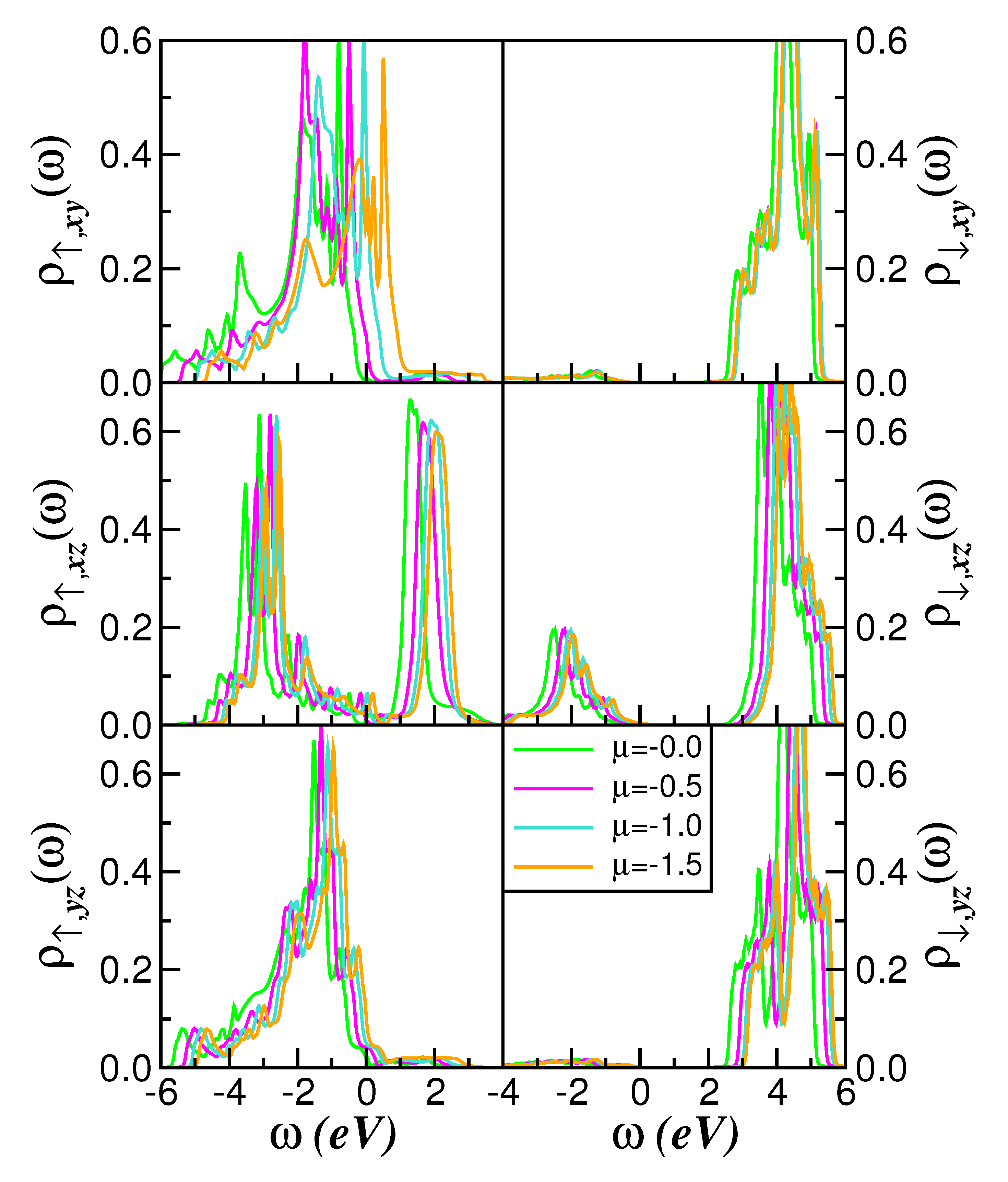
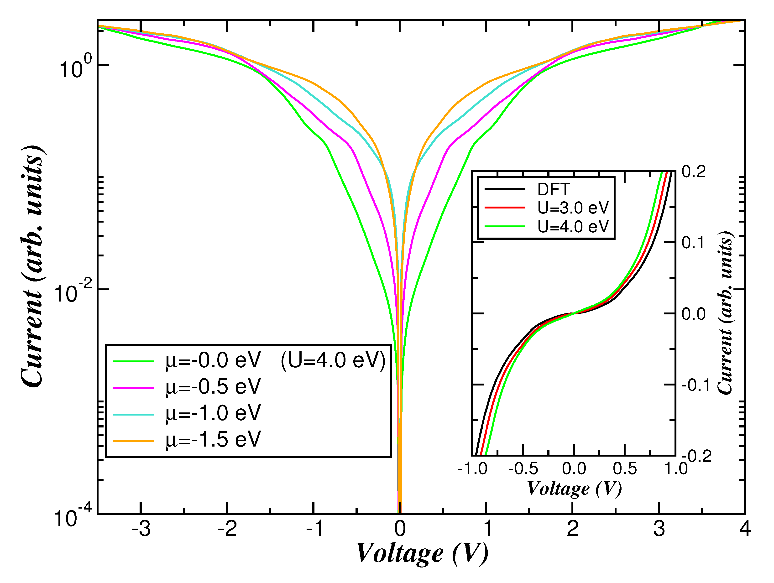
2. Results and Discussion

The DFT calculations in this work were performed for the FM phase of orthorhombic CrSBr bulk crystal using the SIESTA ab initio simulation package [46] (code 4.1.5). The generalized gradient approximation (GGA) in the PBE implementation [47] was applied as the exchange correlation functional. Norm-conserving pseudopotentials in the nonlocal form [48] were used to represent the ionic core potential. Additionally, the Kohn–Sham orbitals [49] were expanded in a linear combination of atomic orbitals of finite range, which is determined by an energy shift of 0.01 R y [50]. The real-space grid integration was determined by an energy cutoff of 200 R y [51]. The respective Brillouin zone was sampled by a 10 × 10 × 10 grid [52] for a primitive cell of bulk CrSBr. In this work, all lattice constants were taken from Ref. [21], and similar to Ref. [6], the atomic positions are fully optimized until all the force components became smaller than 0.03 eV/Å.
Earlier DFT + DMFT-based studies have shown how the electronic state changes across the magnetic [53,54] phase transition and why they can be semiquantitatively understood using DFT + DMFT using sizable local, MO correlations. Here, we extend this perspective and characterize the t 2 g electronic and electrical properties of FM CrSBr bulk crystal, revealing the fingerprints of spin- and orbital-selective semiconductivity. With this in mind, in Figure 2 we show the GGA density of state (DOS) of the majority (↑) and minority (↓) spin channels of FM CrSBr within the t 2 g orbital sector relevant for the C r 3 + oxidation. As for ferromagnetic systems, the majority spin band is transferred to lower binding energies as a result of the magnetic transition, while the minority spin channel is depopulated due to large spin splitting of the FM phase. Taken together with earlier studies on Cr-containing materials [5,55], our GGA results in Figure 2 reveal strong spin-orbital differentiation in the FM CrSBr semiconductor, which, as shown here, leads to decreased electron correlation effects through increasing the one-particle bandwidth, undoubtedly a feature that could be seen in future experiments by tuning the PM-to-FM phase boundary. The most salient result in Figure 2 is the band broadening observed in the GGA DOS, which, as a consequence, is expected to induce the partial screening of the Coulomb potential [56]. CrSBr is similar to that reported for BiFeO3 [54]. Motivated thereby, below we show how DFT + DMFT [40] modifies the GGA band structure of FM CrSBr bulk crystal.
Within GGA, the one-electron part of the MO- t 2 g Hamiltonian for CrSBr reads H 0 = k , a , σ ϵ a ( k ) c k , a , σ c k , a , σ μ i , α , a , σ n i , α , a , σ , where a = x z , y z , x y denote the diagonalized t 2 g orbitals, ϵ a ( k ) is the band dispersion, and μ is the chemical potential. Below, these three Cr- 3 d MO-orbital states will be used as the bare one-particle inputs to MO-DMFT, which generates a weakly correlated electronic state. Local MO interactions in FM CrSBr bulk crystal are given in H i n t [5,54,55], which contains the on-site Hubbard–Coulomb interaction U, the inter-orbital Coulomb interaction term U = U 2 J H , and the Hund’s coupling J H . We evaluate self-consistently the many-particle Green’s functions of the MO Hamiltonian H = H 0 + H i n t within DFT + DMFT [40], using MO iterated perturbation theory (MO-IPT) as the impurity solver [57]. The IPT (MO or not) impurity solver is an interpolative ansatz that accounts for the correct low- and high-energy behavior of the one-particle spectral functions in Hubbard- and Anderson-like models in the infinity dimensional lattice limit (DMFT). It ensures the Mott–Hubbard metal-insulator transition from a correlated metal to a Mott insulator is a function of the on-site Hubbard–Coulomb interaction U. This perturbative many-particle scheme is computationally efficient, with real frequency output both at zero and non-zero temperatures, and it can provide results that are in qualitatively good accord with numerically exact quantum Monte Carlo (QMC) calculations for real one-band [58] and MO [59,60] systems.
Although the fundamental problem of the stability of semiconductors against many-particle correlation effects is under debate [61,62,63], we shall notice that electron interactions may give rise to nontrivial electronic reconstruction and single-particle electronic excitations in broadband semiconductors, which, as shown here, is not the case from FM CrSBr due to intrinsic strong spin polarization at the bare one-particle level. With these caveats, let us now turn our attention to our DFT + DMFT (MO-IPT) results obtained within the formal C r 3 + oxidation state of the FM CrSBr parent compound. In Figure 2, we display the combined-effect MO dynamical correlations on the orbital- and spin-resolved t 2 g spectral functions of FM CrSBr, showing their weakly electronic structure reconstruction induced by MO electron–electron correlation effects in the real solid. As seen, small changes in the majority x y ,   y z orbitals are manifested at high binding energies below the Fermi level ( E F = ω = 0.0 ) . At the fixed J H = 0.7 eV orbital, selectivity develops with the emergence of incoherent and lower Hubbard bands below 3.0 eV binding energy in the majority x y and y z channels: a feature that has not been reported in the extant literature of FM CrSBr bulk crystal down to its 2D limit. Moreover, as seen in Figure 2, the minority spin states are nearly unaffected when the on-site Coulomb interaction U is increased, suggesting that the majority t 2 g orbitals are the only active channels in FM CrSBr, a behavior similar to that reported based on DFT + DMFT for FM CrO2 [55].
The most relevant features in Figure 2 are the clearly visible stability of the semiconducting spectrum against MO electron–electron interactions. This effect is also manifested in the changes in the orbital-resolved self-energy imaginary parts in Figure 3, where the emergent correlated semiconducting state is characterized by the absence of electronic excitation within the low energy window where I m Σ a , σ ( ω ) vanishes. Interestingly, the ω -dependence of the I m Σ a , σ ( ω ) we derive for FM CrSBr in the clean limit is similar to that found for the extended periodic Anderson model [57], a model relevant to understanding the stability of the Kondo-insulating state against electron–electron interactions [64]. Importantly, the Kondo insulators are correlated electron systems [65] whose PM low-energy excitations and normal state properties are directly connected to noninteracting semiconductors [66]. Hence, they can be seen as a continued many-particle version of bare band insulators, where dynamical correlations are manifested above the one-particle bandgap scale.
However, in order to provide additional insights into our weakly electronic structure reconstruction in FM CrSBr, in Figure 4 we display the DFT and DFT + DMFT (MO-IPT) t 2 g total spectral functions [ ρ t o t a l ( ω ) = a , σ ρ a , σ ( ω ) ] , showing good qualitative agreement between the two. Particularly interesting in this figure is the DFT bandgap and the total spectral function lineshape, the latter almost coinciding with the d I / d V spectrum of Ref. [25] after reversing the sign of the bias polarity in the experimental curve. Importantly, looking at both the conduction and valence band states close to E F reveals an U-shaped like bandgap similar to that observed at 7 K in Ref. [67]. Future angle-integrated photoemission spectroscopy (PES) and inverse-PES are called for to corroborate our selective electronic structure reconstruction and the presence of incoherent lower Hubbard bands at high binding energies within a weakly correlated semiconducting state from 150 K down to low temperatures in CrSBr.
Motivated by recent studies reporting lithium-ion intercalation on both AFM [67] and FM [68] CrSBr, in Figure 5 we reveal the changes of the orbital- and spin-resolved DFT + DMFT DOS upon doping of the FM CrSBr bulk crystal. We shall notice here that according to Ref. [67], Li-intercalation transforms CrSBr from an AFM semiconductor into an FM metal, and a charge density wave (CDW) order that remains stable up to room T. Ignoring for simplicity the CDW ordered state [69], and considering a fixed U = 4.0 eV as in Ref. [67] as a representative on-site Coulomb interaction parameter for magnetic CrSBr, in Figure 5 we show the doping dependence of the orbital- and spin-resolved spectral functions of FM CrSBr. As seen, when the total band filling upon changing the chemical potential μ of the system is increased, the valence band states are dynamically transferred to energies above E F with concomitant depletion of the lower Hubbard band in the majority x y channel of stoichiometric ( μ = 0 ) CrSBr. This, together with the suppression of the upper Hubbard band in the majority x z orbital, comprises microscopic one-particle signatures of reduced electronic correlations in doped CrSBr, an effect which might open the way towards the emergence of a CDW ordered state in Li-CrSBr [67] via electron-lattice [70] or other residual [71,72] interactions. Interestingly, looking at our results in Figure 5 and scanning the tunneling spectroscopy (STS) data of Li-CrSBr of Ref. [67] suggests that the semiconducting gap filling or the non-zero DOS at all energies reported in this recent STS study might be linked to the electronic states of the majority x y , which shows the presence of in-gap modes above E F at large μ arising as a result of doping of the parent compound.
Finally, in order to shine light on the role played by doping effects on the changes in the Cr-based current–voltage (IV) characteristic reported earlier for PM CrSBr [39], in Figure 6 we present our the DFT + DMFT results using the correlated spectral functions computed for U = 4.0 eV and the different μ values considered in Figure 5. Within the wideband limit of the left (L) and right (R) electrodes, the current formula for a tunneling experiment can be written as I = 2 e a , σ d ω Γ ˜ ( ω ) f L ( ω ) f R ( ω ) ρ a , σ ( ω ) [73,74], where Γ ˜ ( ω ) = Γ L ( ω ) Γ R ( ω ) / Γ ( ω ) with Γ α ( ω ) = π k | t k α | 2 δ ( ω ε k α ) being the coupling strength between electrode α and the central region [75,76], and Γ ( ω ) = Γ L ( ω ) + Γ R ( ω ) . f α ( ω ) = 1 / ( e β ( ω μ α ) + 1 ) and ρ a , σ ( ω ) = 1 π I m G a , σ ( ω ) are, respectively, the Fermi function of the electrode α and the total DOS of the Cr- 3 d t 2 g channel with spin- σ of FM CrSBr. Secondly, here we assume a symmetric voltage drop, μ L = μ R = e V , and a constant DOS for the wideband limit of the leads: these assumptions give a microscopic description [77] of the current–voltage characteristic of CrSBr memristor [39].
In the main panel and at the inset of Figure 6, we show, respectively, the semi-logarithmic and linear current–voltage (IV) characteristic curves obtained using the orbital-resolved DFT + DMFT DOS shown in Figure 5. As seen, FM CrSBr exhibits memristive behavior similar to that reported in extant experimental studies in the PM phase [39], where the resistance steady-state value exhibits an ON/OFF ratio of 10 3 assisted by n-type doping. Our results in the main panel of Figure 6 suggest that doped CrSBr memristor [39] exhibits resistive analog memory with unipolar (or symmetric), low-resistance state (LRS), and high-resistance state (HRS). However, unlike the theory IV characteristic shown in the main panel and inset of Figure 6, which does not depend on the polarity of the voltage and current signal, in the experiment the IV characteristic of CrSBr and analogs is in most cases bipolar (or antisymmetric), since during switching the set to an ON state occurs at one voltage polarity and the reset to the OFF state on reversed voltage polarity [78]. This is linked to the fact that the structure of the real system has some intrinsic asymmetry arising from different electrode materials or the voltage polarity during the initial electroforming cicle [78], resulting in a bipolar switching behavior. According to the DFT + DMFT results, the unipolar switching in FM CrSBr is predicted to be due to channel-selective n-doping upon Li-deintercalation, resulting in an analog memristive functionality of FM Li-CrSBr for memory-based neuromorphic computing [79,80,81,82].
Notably, our results show similar changes in the IV loops to in PM CrSBr at positive voltages as in Ref. [39], and more importantly, they indicate that the nonvolatile sweep cycle [79,80] could be made by tuning the Li concentration in FM Li-CrSBr bulk crystal. Also interesting in our results in the main panel of Figure 6 are the changes in selectivity as well as in the voltage window, with the latter being consistent with those reported for other memristor compounds [81,82]. During the applied voltage swept from 0 V to ± 2.0 V and starting in the lower doping regime, the current increases when the voltage reaches a threshold value. At this point, the system changes its metallic state as shown in Figure 5, implying that the selector in future experiments may switch from a nearly OFF state, reaching an ON state. Similar to nonvolatile systems, after reaching a current plateau the current reduces as the applied voltage sweeps back to the hold voltage, meaning that FM CrSBr memristor changes to a less metallic state and the device returned to OFF state at low voltages. As mentioned above within our theory, the system performs similarly at positive and negative voltage areas due to its symmetrical characteristics [83]. As in Ref. [77], here the IV characteristic is mainly defined by the bulk electronic state giving rise to symmetric results for positive and negative voltage polarity, while in the experiment the inhomogeneity is likely to arise from the different nature of the electrodes apart from intrinsic disorder, domain formation, or strain in the lithiated crystal [67]. However, our results in the main panel of Figure 6 suggest that the changes of the total t 2 g electron band filling of FM CrSBr upon lithiation (or ion extraction/intercalation) would induce selector memristive behavior for brain-inspired neuromorphic computing [84].

3. Conclusions

In summary, in this work we use GGA and GGA + DMFT results for understanding the electronic structure of the bulk CrSBr compound in its ferromagnetically ordered state. Using realistic local Hubbard–Coulomb interaction parameters in the three-orbital Hubbard model of CrSBr, we set up a microscopic description of the weakly correlated excitation spectrum that emerges in this van der Waals lattice system. Our theory analysis is expected to be generally applicable to understanding the emergent selectivity in correlated systems and the electronic spectra that emerges in van der Waals magnetic materials upon doping [67,68]. This work is a step forward in understanding the manifestation of orbital- and spin-selectivity, which might form a basis to predict the IV responses of future FM CrSBr memristor. The presented theoretical picture indicates how chemical doping leads to volatile memristive functionality, placing air stable CrSBr bulk crystal as a candidate material for the development of all-spin neuromorphic hardware [85].

Author Contributions

L.C. and S.S.C., conceptualization, methodology, writing, and editing. All authors have read and agreed to the published version of the manuscript.

Funding

This research received no external funding.

Data Availability Statement

Data available upon request to the authors.

Acknowledgments

Acknowledgement is made of CNPq and CAPES as well as of Byron Freelon for discussions.

Conflicts of Interest

The authors declare no conflicts of interest.

References

  1. Novoselov, K.S.; Geim, A.K.; Morozov, S.V.; Jiang, D.; Zhang, Y.; Dubonos, S.V.; Grigorieva, I.V.; Firsov, A. A Electric field effect in atomically thin carbon films. Science 2004, 306, 666. [Google Scholar] [CrossRef] [PubMed]
  2. Long, F.; Mosina, K.; Hübner, R.; Sofer, Z.; Klein, J.; Prucnal, S.; Helm, M.; Dirnberger, F.; Zhou, S. Intrinsic magnetic properties of the layered antiferromagnet CrSBr. Appl. Phys. Lett. 2023, 123, 222401. [Google Scholar] [CrossRef]
  3. Huang, B.; Clark, G.; Navarro-Moratalla, E.; Klein, D.R.; Cheng, R.; Seyler, K.L.; Zhong, D.; Schmidgall, E.; McGuire, M.A.; Cobden, D.H.; et al. Layer-dependent ferromagnetism in a van der Waals crystal down to the monolayer limit. Nature 2017, 546, 265. [Google Scholar] [CrossRef] [PubMed]
  4. Gong, G.; Li, L.; Li, Z.; Ji, H.; Stern, A.; Xia, Y.; Cao, T.; Bao, W.; Wang, C.; Wang, Y.; et al. Discovery of intrinsic ferromagnetism in two-dimensional van der Waals crystals. Nature 2017, 546, 265. [Google Scholar] [CrossRef]
  5. Craco, L.; Carara, S.S.; Shao, Y.-C.; Chuang, Y.-D.; Freelon, B. Mott localization in the van der Waals crystal CrI3: A GGA + DMFT study. Phys. Rev. B 2020, 102, 195130. [Google Scholar] [CrossRef]
  6. Craco, L.; Carara, S.S.; Shao, Y.-C.; Chuang, Y.-D.; Freelon, B. Electronic structure of rhombohedral CrX3 (X = Br, Cl, I) van der Waals crystals. Phys. Rev. B 2021, 103, 235119. [Google Scholar] [CrossRef]
  7. Wang, Q.H.; Bedoya-Pinto, A.; Blei, M.; Dismukes, A.H.; Hamo, A.; Jenkins, S.; Koperski, M.; Liu, Y.; Sun, Q.C.; Telford, E.J.; et al. The magnetic genome of two-dimensional van der Waals materials. ACS Nano 2020, 16, 6960. [Google Scholar] [CrossRef]
  8. Wolf, S.A.; Awschalom, D.D.; Buhrman, R.A.; Daughton, J.M.; Molnar, S.V.; Roukes, M.L.; Chtchelkanova, Y.A.; Treger, D.M. Spintronics: A spin-based electronics vision for the future. Science 2021, 294, 1488. [Google Scholar] [CrossRef]
  9. Awschalom, D.D.; Flatté, M.E. Challenges for semiconductor spintronics. Nat. Phys. 2007, 3, 153. [Google Scholar] [CrossRef]
  10. Li, H.; Ruan, S.; Zeng, Y.J. Intrinsic van der Waals magnetic materials from bulk to the 2D limit: New frontiers of spintronics. Adv. Mater. 2019, 31, 1900065. [Google Scholar] [CrossRef]
  11. Jin, C.; Lin, F.; Suenaga, K.; Iijima, S. Fabrication of a freestanding boron nitride single layer and its defect assignments. Phys. Rev. Lett. 2009, 102, 195505. [Google Scholar] [CrossRef] [PubMed]
  12. Splendiani, A.; Sun, L.; Zhang, Y.; Li, T.; Kim, J.; Chim, C.Y. Emerging photoluminescence in monolayer MoS2. Nano Lett. 2010, 10, 1271–1275. [Google Scholar] [CrossRef] [PubMed]
  13. Li, T.; Galli, G. Electronic properties of MoS2 nanoparticles. J. Phys. Chem. C 2007, 111, 16192. [Google Scholar] [CrossRef]
  14. Upreti, D.; Basnet, R.; Sharma, M.M.; Chhetri, S.K.; Acharya, G.; Nabi, M.R.U.; Sakon, J.; Da, B.; Mortazavin, M.; Hu, J. Tuning magnetism in Ising-type van der Waals magnet FePS3 by lithium intercalation. J. Phys. Condens. Matter 2025, 37, 135805. [Google Scholar] [CrossRef]
  15. Basnet, R.; Upreti, D.; Patel, T.; Karki Chhetri, S.; Acharya, G.; Nabi, M.R.U.; Sharma, M.M.; Sakon, J.; Mortazavi, M.; Hu, J. Field-induced spin polarization in the lightly Cr-substituted layered antiferromagnet NiPS3. Phys. Rev. B 2024, 109, 184405. [Google Scholar] [CrossRef]
  16. Dinesh Upreti, D.; Basnet, R.; Sharma, M.M.; Chhetri, S.K.; Acharya, G.; Nabi, M.R.U.; Sakon, J.; Benamara, M.; Mortazavi, M.; Jin, H. Medium-entropy engineering of magnetism in layered antiferromagnet CuxNi2(1−x)CrxP2S6. Adv. Func. Mater. 2024, 35, 2418722. [Google Scholar] [CrossRef]
  17. Wang, F.; Mathur, N.; Janes, A.N.; Sheng, H.; He, P.; Zheng, X.; Yu, P.; DeRuiter, A.J.; Schmidt, J.R.; He, J.; et al. Defect-mediated ferromagnetism in correlated two-dimensional transition metal phosphorus trisulfides. Sci. Adv. 2021, 7, eabj4086. [Google Scholar] [CrossRef]
  18. Odile, J.P.; Steger, J.J.; Wold, A. Preparation and properties of the solid solution series zinc iron phosphorus trisulfide (Zn1−xFexPS3). Inorg. Chem. 1975, 14, 2400. [Google Scholar] [CrossRef]
  19. Han, H.; Lin, H.; Gan, W.; Liu, Y.; Xiao, R.; Zhang, L.; Li, Y.; Zhang, C.; Li, H. Emergent mixed antiferromagnetic state in MnPS3(1−x)Se3x. Appl. Phys. Lett. 2023, 122, 033101. [Google Scholar] [CrossRef]
  20. Mi, M.; Zheng, X.; Wang, S.; Zhou, Y.; Yu, L.; Xiao, H.; Song, H.; Shen, B.; Li, F.; Bai, L.; et al. Variation between antiferromagnetism and ferrimagnetism in NiPS3 by electron doping. Adv. Funct. Mater. 2022, 32, 2112750. [Google Scholar] [CrossRef]
  21. Göser, O.; Paul, W.; Kahle, H.G. Magnetic properties of CrSBr. J. Magn. Magn. Mater. 1990, 92, 129. [Google Scholar] [CrossRef]
  22. Song, C.; Bai, H.; Zhou, Z.; Han, L.; Reichlova, H.; Dil, J.H.; Liu, J.; Chen, X.; Pan, F. Altermagnets as a new class of functional materials. Nat. Rev. Mater. 2025. in print. [Google Scholar] [CrossRef]
  23. Pei, F.; Yu, J.; Zhou, J.; Wang, S.; Liu, D.; Yuan, Y.; Xi, L.; Jin, F.; Kan, X.; Wang, C.; et al. Surface-sensitive detection of magnetic phase transition in van Der Waals magnet CrSBr. Adv. Funct. Mater. 2024, 34, 2309335. [Google Scholar] [CrossRef]
  24. Scheie, A.; Ziebel, M.; Chica, D.G.; Bae, Y.J.; Wang, X.; Kolesnikov, A.I.; Zhu, X.; Roy, X. Spin Waves and Magnetic Exchange Hamiltonian in CrSBr. Adv. Sci. 2022, 9, 2202467. [Google Scholar] [CrossRef]
  25. Telford, E.J.; Dismukes, A.H.; Lee, K.; Cheng, M.; Wieteska, A.; Bartholomew, A.K.; Chen, Y.-S.; Xu, X.; Pasupathy, A.N.; Zhu, X.; et al. Layered antiferromagnetism induces large negative magnetoresistance in the van der Waals Semiconductor CrSBr. Adv. Mater. 2020, 32, 2003240. [Google Scholar] [CrossRef]
  26. Lee, K.; Dismukes, A.H.; Telford, E.J.; Wiscons, R.A.; Wang, J.; Xu, X.; Nuckolls, C.; Dean, C.R.; Roy, X.; Zhu, X. Magnetic order and symmetry in the 2D semiconductor CrSBr. Nano Lett. 2021, 21, 3511. [Google Scholar] [CrossRef]
  27. Liu, W.; Guo, X.; Schwartz, J.; Xie, H.; Dhale, N.U.; Sung, S.H.; Kondusamy, A.L.N.; Wang, X.; Zhao, H.; Berman, D.; et al. A three-stage magnetic phase transition revealed in ultrahigh-quality van der Waals bulk magnet CrSBr. ACS Nano 2022, 6, 15917. [Google Scholar] [CrossRef]
  28. Rizzo, D.J.; McLeod, A.S.; Carnahan, C.; Telford, E.J.; Dismukes, A.H.; Wiscons, R.A.; Dong, Y.; Nuckolls, C.; Dean, C.R.; Pasupathy, A.N.; et al. Visualizing atomically layered magnetism in CrSBr. Adv. Mater. 2022, 34, 2201000. [Google Scholar] [CrossRef]
  29. Telford, E.J.; Dismukes, A.H.; Dudley, R.L.; Wiscons, R.A.; Lee, K.; Chica, D.G.; Ziebel, M.E.; Han, M.-G.; Yu, J.; Shabani, S.; et al. Coupling between magnetic order and charge transport in a two-dimensional magnetic semiconductor. Nat. Mater. 2022, 21, 754. [Google Scholar] [CrossRef]
  30. Klein, J.; Song, Z.; Pingault, B.; Dirnberger, F.; Chi, H.; Curtis, J.B.; Dana, R.; Bushati, R.; Quan, J.; Dekanovsky, L.; et al. Sensing the local magnetic environment through optically active defects in a layered magnetic semiconductor. ACS Nano 2023, 17, 288. [Google Scholar] [CrossRef]
  31. Wu, F.; Gutierrez-Lezama, I.; Lopez-Paz, S.A.; Gibertini, M.; Watanabe, K.; Taniguchi, T.; von Rohr, F.O.; Ubrig, N.; Morpurgo, A.F. Quasi-1D electronic transport in a 2D magnetic semiconductor. Adv. Mater. 2022, 34, 2109759. [Google Scholar] [CrossRef] [PubMed]
  32. Lopez-Paz, S.A.; Guguchia, Z.; Pomjakushin, V.Y.; Witteveen, C.; Cervellino, A.; Luetkens, H.; Casati, N.; Morpurgo, A.F.; von Rohr, F.O. Dynamic magnetic crossover at the origin of the hidden-order in van der Waals antiferromagnet CrSBr. Nat. Commun. 2022, 13, 4745. [Google Scholar] [CrossRef] [PubMed]
  33. Boix-Constant, C.; Manas-Valero, S.; Ruiz, A.M.; Rybakov, A.; Konieczny, K.A.; Pillet, S.; Baldovi, J.J.; Coronado, E. Probing the spin dimensionality in single-layer CrSBr van der Waals heterostructures by magneto-transport measurements. Adv. Mater. 2022, 34, 2204940. [Google Scholar] [CrossRef] [PubMed]
  34. Beck, J. Über chalkogenidhalogenide des Chroms synthese, kristallstruktur und magnetismus von chromsulfidbromid, CrSBr. Z. Anorg. Allg. Chem. 1990, 585, 157. [Google Scholar] [CrossRef]
  35. Jo, J.; Mañas-Valero, S.; Coronado, E.; Casanova, F.; Gobbi, M.; Hueso, L.E. Nonvolatile electric control of antiferromagnet CrSBr. Nano Lett. 2024, 24, 4471. [Google Scholar] [CrossRef]
  36. Ziebel, M.E.; Feuer, M.L.; Cox, J.; Zhu, X.; Dean, C.R.; Roy, X. CrSBr: An air-stable, two-dimensional magnetic semiconductor. Nano Lett. 2024, 24, 4319. [Google Scholar] [CrossRef]
  37. Liu, Z.; Zhu, C.; Gao, Y.; Chen, Z.; Gu, P.; Te, Y. Probing spin textures in atomically thin CrSBr through tunneling magnetoresistance. arXiv 2024, arXiv:2407.13230. [Google Scholar]
  38. Yang, B.; Bhujel, B.; Chica, D.G.; Telford, E.J.; Roy, X.; Ibrahim, F.; Chshiev, M.; Cosset-Chéneau, M.; van Wees, B.J. Electrostatically controlled spin polarization in graphene-CrSBr magnetic proximity heterostructures. Nat. Commun. 2024, 15, 4459. [Google Scholar] [CrossRef]
  39. Li, Z.; Liu, R.; Chu, Y.; Feng, S.; Lan, W.; Duan, H.; Liu, C.; Yan, W. Dual-terminal artificial synapse in two-dimensional CrSBr memristor for neuromorphic computing. J. Mater. Sci. Mater Electron 2024, 35, 1091. [Google Scholar] [CrossRef]
  40. Kotliar, G.; Savrasov, S.Y.; Haule, K.; Oudovenko, V.S.; Parcollet, O.; Marianetti, C.A. Electronic structure calculations with dynamical mean-field theory. Rev. Mod. Phys. 2006, 78, 865. [Google Scholar] [CrossRef]
  41. Wilson, N.P.; Lee, K.; Cenker, J.; Xie, K.; Dismukes, A.H.; Telford, E.J.; Fonseca, J.; Sivakumar, S.; Dean, C.; Cao, T.; et al. Interlayer electronic coupling on demand in a 2D magnetic semiconductor. Nat. Mater. 2021, 20, 1657. [Google Scholar] [CrossRef] [PubMed]
  42. Wang, Y.; Luo, N.; Zeng, J.; Tang, L.-M.; Chen, K.-Q. Magnetic anisotropy and electric field induced magnetic phase transition in the van der Waals antiferromagnet CrSBr. Phys. Rev. B 2023, 108, 054401. [Google Scholar] [CrossRef]
  43. Guo, H.-T.; Guo, S.-D.; Ang, Y.S. Electric-field induced half-metal in monolayer CrSBr. arXiv 2023, arXiv:2308.03430. [Google Scholar]
  44. Bo, X.; Li, F.; Xu, X.; Wan, X.; Pu, Y. Calculated magnetic exchange interactions in the van der Waals layered magnet CrSBr. New J. Phys. 2023, 25, 013026. [Google Scholar] [CrossRef]
  45. Yang, K.; Wang, G.; Liu, L.; Lu, D.; Wu, H. Triaxial magnetic anisotropy in the two-dimensional ferromagnetic semiconductor CrSBr. Phys. Rev. B 2021, 104, 144416. [Google Scholar] [CrossRef]
  46. Soler, J.M.; Artacho, E.; Gale, J.D.; García, A.; Junquera, J.; Ordejón, P.; Sánchez-Portal, D. The SIESTA method for ab initio order-N materials simulation. J. Phys. Condens. Matter 2002, 14, 2745. [Google Scholar] [CrossRef]
  47. Perdew, J.P.; Burke, K.; Ernzerhof, M. Generalized gradient approximation made simple. Phys. Rev. Lett. 1996, 77, 3865. [Google Scholar] [CrossRef]
  48. Troullier, N.; Martins, J.L. Efficient pseudopotentials for plane-wave calculations. Phys. Rev. B 1991, 43, 1993. [Google Scholar] [CrossRef]
  49. Kohn, W.; Sham, L.J. Self-consistent equations including exchange and correlation effects. Phys. Rev. 1965, 140, A1133. [Google Scholar] [CrossRef]
  50. Junquera, J.; Paz, Ó.; Sánchez-Portal, D.; Artacho, E. Numerical atomic orbitals for linear-scaling calculations. Phys. Rev. B 2001, 64, 235111. [Google Scholar] [CrossRef]
  51. Moreno, J.; Soler, J.M. Optimal meshes for integrals in real- and reciprocal-space unit cells. Phys. Rev. B 1992, 45, 13891. [Google Scholar] [CrossRef] [PubMed]
  52. Monkhorst, H.J.; Pack, D.J. Special points for Brillouin-zone integrations. Phys. Rev. B 1976, 13, 5188. [Google Scholar] [CrossRef]
  53. Craco, L.; Leoni, S.; Laad, M.S.; Rosner, H. Orbital-selective charge dynamics in YTiO3 across the magnetic transition: Combined local-density approximation and dynamical mean-field theory. Phys. Rev. B 2007, 76, 115128. [Google Scholar] [CrossRef]
  54. Craco, L.; Carara, S.S.; Leoni, S. Electronic structure of BiFeO3 in the presence of strong electronic correlations. Phys. Rev. B 2019, 99, 045112. [Google Scholar] [CrossRef]
  55. Craco, L.; Laad, M.S.; Müller-Hartmann, E. Orbital Kondo effect in CrO2: A combined local-spin-density-approximation dynamical-mean-field-theory study. Phys. Rev. Lett. 2003, 90, 237203. [Google Scholar] [CrossRef]
  56. Muneta, I.; Ohya, S.; Terada, H.; Tanaka, M. Sudden restoration of the band ordering associated with the ferromagnetic phase transition in a semiconductor. Nature Commun. 2016, 7, 12013. [Google Scholar] [CrossRef]
  57. Craco, L. Quantum orbital entanglement: A view from the extended periodic Anderson model. Phys. Rev. B 2008, 77, 125122. [Google Scholar] [CrossRef]
  58. Craco, L.; Carara, S.S.; de Arruda, A.S.; de Arruda, P.H.Z.; Leoni, S. Tunable analog and nearly digital responses in hole-doped LiNbO2 memristors. Solid State Commun. 2025, 401, 115911. [Google Scholar] [CrossRef]
  59. Craco, L.; Leoni, S. Theory of two-fluid metallicity in superconducting FeSe at high pressure. Phys. Rev. B 2019, 100, 121101. [Google Scholar] [CrossRef]
  60. Craco, L.; Leoni, S. Mott and pseudogap localization in pressurized NbO2. Phys. Rev. B 2020, 102, 045142. [Google Scholar] [CrossRef]
  61. Hybertsen, M.S.; Louie, S.G. Electron correlation in semiconductors and insulators: Band gaps and quasiparticle energies. Phys. Rev. B 1986, 34, 5390. [Google Scholar] [CrossRef] [PubMed]
  62. Chemla, D.S.; Shah, J. Many-body and correlation effects in semiconductors. Nature 2001, 411, 549. [Google Scholar] [CrossRef] [PubMed]
  63. Tuan, D.V.; Dery, H. Excitons and trions in monolayer semiconductors with correlated electrons. Phys. Rev. B 2023, 108, 085303. [Google Scholar] [CrossRef]
  64. Koga, A.; Kawakami, N.; Peters, R.; Pruschke, T. Quantum phase transitions in the extended periodic Anderson model. Phys. Rev. B 2008, 77, 045120. [Google Scholar] [CrossRef]
  65. Martin, R.; Allen, J. Theory of mixed valence: Metals or small gap insulators. J. Appl. Phys. 1979, 50, 7561. [Google Scholar] [CrossRef]
  66. Dzero, M.; Sun, K.; Galitski, V.; Coleman, P. Topological Kondo Insulators. Phys. Rev. Lett. 2010, 104, 106408. [Google Scholar] [CrossRef]
  67. Feuer, M.L.; Thinel, M.; Huang, X.; Cui, Z.-H.; Shao, Y.; Kundu, A.K.; Chica, D.G.; Han, M.-G.; Pokratath, R.; Telford, E.J.; et al. Doping-induced charge density wave and ferromagnetism in the van der Waals semiconductor CrSBr. Adv. Mater. 2025, 2418066. [Google Scholar] [CrossRef]
  68. Mosina, K.; Wu, B.; Antonatos, N.; Luxa, J.; Mazánek, V.; Söll, A.; Sedmidubsky, D.; Klein, J.; Ross, F.M.; Sofer, Z. Electrochemical intercalation and exfoliation of CrSBr into ferromagnetic fibers and nanoribbons. Small Methods 2024, 8, 2300609. [Google Scholar] [CrossRef]
  69. Craco, L. Two-band electronic reconstruction induced via correlation and CDW order effects. Condens. Matter 2024, 9, 42. [Google Scholar] [CrossRef]
  70. Rossnagel, K. On the origin of charge-density waves in select layered transition-metal dichalcogenides. J. Phys. Condens. Matter 2011, 23, 213001. [Google Scholar] [CrossRef]
  71. Torres, T.; Kuc, A.; Maschio, L.; Pham, T.; Reidy, K.; Dekanovsky, L.; Sofer, Z.; Ross, F.M.; Klein, J. Probing defects and spin-phonon coupling in CrSBr via resonant Raman scattering. Adv. Funct. Materails 2023, 3, 2211366. [Google Scholar] [CrossRef]
  72. Souza, I.J.; de Arruda, P.H.Z.; Godoy, M.; Craco, L.; de Arruda, A.S. Random crystal-field effects in a mixed spin-1 and spin-3/2 ferrimagnetic Ising system. Physica A 2016, 44, 589. [Google Scholar] [CrossRef]
  73. Meir, Y.; Wingreen, N.S. Landauer formula for the current through an interacting electron region. Phys. Rev. Lett. 1992, 68, 2512. [Google Scholar] [CrossRef] [PubMed]
  74. Craco, L.; Kang, K. Perturbation treatment for transport through a quantum dot. Phys. Rev. B 1999, 59, 12244. [Google Scholar] [CrossRef]
  75. Cuniberti, G.; Craco, L.; Porath, D.; Dekker, C. Backbone-induced semiconducting behavior in short DNA wires. Phys. Rev. B 2002, 65, 241314(R). [Google Scholar] [CrossRef]
  76. Bao, X.-X.; Wang, X.-F. Effects of long-range dispersive interaction on the electron transport in short single strands of guanine bases. Int. J. Quantum Chem. 2023, 1, e27251. [Google Scholar] [CrossRef]
  77. Craco, L.; Chagas, E.F.; Carara, S.S.; Freelon, B. Atomristor Mott theory of Sn adatom adlayer on a Si surface. Condens. Matter 2024, 9, 32. [Google Scholar] [CrossRef]
  78. Waser, R.; Aono, M. Nanoionics-based resistive switching memories. Nat. Mater. 2007, 6, 833. [Google Scholar] [CrossRef]
  79. Wang, R.; Yang, J.-Q.; Mao, J.-Y.; Wang, Z.-P.; Wu, S.; Zhou, M.; Chen, T.; Zhou, Y.; Han, S.-T. Recent advances of volatile memristors: Devices, mechanisms, and applications. Adv. Intell. Syst. 2020, 2, 202000055. [Google Scholar] [CrossRef]
  80. Sangwan, V.K.; Hersam, M.C. Neuromorphic nanoelectronic materials. Nat. Nanotechnol. 2020, 15, 517. [Google Scholar] [CrossRef]
  81. Song, M.-K.; Kang, J.-H.; Zhang, X.; Ji, W.; Ascoli, A.; Messaris, I.; Demirkol, A.S.; Dong, B.; Aggarwal, S.; Wan, W.; et al. Recent advances and future prospects for memristive materials, devices, and systems. ACS Nano 2023, 17, 11994. [Google Scholar] [CrossRef] [PubMed]
  82. Ran, Y.; Pei, Y.; Zhou, Z.; Wang, H.; Sun, Y.; Wang, Z.; Hao, M.; Zhao, J.; Chen, J.; Yan, X. A review of Mott insulator in memristors: The materials, characteristics, applications for future computing systems and neuromorphic computing. Nano Res. 2023, 16, 1165. [Google Scholar] [CrossRef]
  83. Chen, A.; Fu, Y.; Yang, G.; Liu, N.; Zhao, X.; Zhang, Z.; Tao, L.; Wan, H.; Rao, Y.; Duan, J.; et al. The Co-improvement of selectivity and uniformity on NbOx-based selector by Al-doping. IEEE Electron Device Lett. 2022, 43, 870. [Google Scholar] [CrossRef]
  84. Mehonic, A.; Ielmini, D.; Roy, K.; Mutlu, O.; Kvatinsky, S.; Serrano-Gotarredona, T.; Linares-Barranco, B.; Spiga, S.; Savel’ev, S.; Balanov, A.G.; et al. Roadmap to neuromorphic computing with emerging technologies. APL Mater. 2024, 12, 109201. [Google Scholar] [CrossRef]
  85. Liu, L.; Wang, D.; Wang, D.; Sun, Y.; Lin, H.; Gong, X.; Zhang, Y.; Tang, R.; Mai, Z.; Hou, Z.; et al. Domain wall magnetic tunnel junction-based artificial synapses and neurons for all-spin neuromorphic hardware. Nat. Commun. 2024, 15, 4534. [Google Scholar] [CrossRef]
Figure 1. Schematic representation of the orthorhombic lattice structure of CrSBr bulk crystal within the paramagnetic (left panel) and ferromagnetic (right panel) ordered phases.
Condensedmatter 10 00027 g001
Figure 2. Comparison between the GGA and GGA + DMFT orbital- and spin-resolved Cr 3 d t 2 g density of states (DOS) of ferromagnetic CrSBr bulk crystal. Important features to note are the strong spin polarization and the small changes in the t 2 g electronic states in the DFT + DMFT results when the on-site Coulomb interaction U is increased.
Condensedmatter 10 00027 g002
Figure 3. Evolution of the GGA + DMFT self-energies imaginary parts as function of the on-site Hubbard–Coulomb interaction U. Notice the weak frequency dependence of I m Σ a , σ ( ω ) within the minority spin channel, a hallmark of spin-polarization-induced dissipation of Coulomb correlation effects in FM CrSBr.
Condensedmatter 10 00027 g003
Figure 4. Total DFT and DFT+DMFT spectral functions of ferromagnetic CrSBr bulk crystal. The narrowing of the semiconducting bandgap in the DFT + DMFT results compared to DFT spectral function is noteworthy.
Condensedmatter 10 00027 g004
Figure 5. Role of doping in the DFT + DMFT results for U = 4.0 eV. Notice the orbital-selective electronic reconstruction within the majority spin channel upon increasing the total band filling of the t 2 g shell of FM CrSBr bulk crystal.
Condensedmatter 10 00027 g005
Figure 6. Evolution of the semi-logarithmic (main panel) and linear (inset) current–voltage (IV) curves of FM CrSBr bulk crystal as function of the chemical potential μ and fixed U = 4.0 eV (main panel) or upon changing the on-site Coulomb interaction U (inset) at zero μ . An interesting feature to be seen is the memristive response with a 10 3 ON/OFF ratio at the main panel.
Condensedmatter 10 00027 g006
Disclaimer/Publisher’s Note: The statements, opinions and data contained in all publications are solely those of the individual author(s) and contributor(s) and not of MDPI and/or the editor(s). MDPI and/or the editor(s) disclaim responsibility for any injury to people or property resulting from any ideas, methods, instructions or products referred to in the content.

