Abstract
Lithium fluoride (LiF) film detectors for extreme ultraviolet radiation, soft and hard X-rays, based on the photoluminescence of radiation-induced electronic defects, have been proposed and are currently under further development and investigation. LiF film detectors are versatile and can be integrated in different experimental apparatus and imaging configurations. LiF can be grown in the form of polycrystalline thin films and it is compatible with several substrates. The radiation-induced color center (CCs) photoluminescence (PL) response can be enhanced through the appropriate choice of substrates and multilayer designs, and by tailoring the micro-structural properties of polycrystalline LiF films through the control of the growth conditions. In this work, we present the characterization, through fluorescence and Raman micro-spectroscopy, of LiF films, thermally evaporated on different substrates with thicknesses of up to 1 μm, irradiated with soft X-rays produced by a laser plasma source. The combination of these micro-spectroscopy techniques could represent an advanced method to investigate the role of the polycrystalline film structures in CC formation efficiency at the microscopic level, a fundamental aspect of the development of LiF film radiation-imaging detectors.
1. Introduction
Point defects (impurity ions, CCs, etc.) in insulating materials [1,2] are successfully used for radiation detectors [3]. Although impressive advances in electronic design and direct detection materials continue to drive progress in the development of radiation-imaging detectors, the role of luminescent materials is still of continued relevance in this field [4]. Pure and doped alkali halide crystals containing CCs represent one of the most investigated fields in solid-state physics connected with optical properties [5]. Among them, CCs in LiF are well known for applications in dosimeters [6], X-ray imaging detectors [7,8,9,10], direct writing of CCs in LiF [11], XFEL beam monitoring [12,13,14], fluorescent nuclear track detectors [15,16], and nuclear sensors for neutrons [17]. These passive solid-state detectors are based on radiation-induced point defects, such as the aggregated F2 and F3+ CCs. These CCs emit broad PL bands at visible wavelengths under blue optical pumping. These defects have almost overlapping broad absorption bands (M band) peaking at approximately 450 nm [18] and, therefore, they can be simultaneously excited with a single-pump wavelength in the blue spectral interval. On the other hand, they exhibit two different Stokes-shifted broad emission bands in the green (F3+) and red (F2) spectral ranges [18]. The peculiar spectroscopic properties of broad-band emitting F2 and F3+ aggregate CCs, which are locally produced by irradiation with ionizing radiations, enable using a simple and efficient optical reading technique, based on fluorescence microscopes.
The growth and characterization of LiF thin films have seen a considerable expansion [19]. LiF film radiation-imaging detectors assure great versatility, as they can be grown by thermal evaporation in the form of optically transparent thin films on different substrates on a wide range of thicknesses (several nm up to several microns) and dimensions (up to several cm2), tailoring the appropriate geometry. Previous works demonstrated that an enhanced sensitivity in LiF film-based detectors can be obtained by tailoring the choice of the substrate materials and the film thickness in the layered imaging detector by taking into account light confinement effects such as in a planar micro-structures [20]. Indeed, the planar structure constituted by the LiF film over the reflective substrate can form an elementary half microcavity, and the thin surface layer containing CCs can be located in proximity to a node of the cavity [20].
Among the main features of CC LiF-based radiation-imaging detectors, there are a large field of view and a wide dynamic range, combined with an intrinsic high spatial resolution, which is in principle limited only by the point defects size, which is at the atomic scale. This means that the resolution is below a few nanometers [21] as the lattice constant of LiF, 0.2013 nm, is the shortest among the alkali halides. In practice, the spatial resolution is limited in the reading stage by the characteristics of the optical microscope and the technique utilized for CC PL detection. LiF-based imaging detectors store the latent image of the exposed sample for a very long time (many years or more) unless heated at high temperatures (>400 °C), thus the X-ray radiography can be read several times, also with different instruments, contrary to the imaging plates currently used at the highest X-ray energies, which suffer from fading effects. LiF film imaging detectors are easy to handle, as they are insensitive to the ambient light (because the F2 and F3+ CCs are stable at RT). Still more practical, they do not need any development process after the exposure, contrary to other imaging detectors such as photographic films and Poly-Metyl-MetAchrilate (PMMA) photoresists.
In this work, LiF films were produced by thermal evaporation on different substrates: glass, silicon, and Al film substrates, at two different thicknesses (up to 1000 nm). LiF films were irradiated with a soft X-ray laser plasma source. After irradiation, the imaging of the visible PL of radiation-induced CCs in LiF films was performed by a confocal laser scanning microscope operating in the fluorescence mode. Moreover, 2D Raman maps of the X-ray-irradiated LiF films were created by a Raman spectrometer combined with a confocal microscope. In LiF, due to the high symmetry of its fcc (face-centered cubic) lattice, the Raman modes are not active at first order. The presence of defects, such as CCs, destroys this symmetry, enabling the observation of Raman spectra also at first order. Raman spectroscopy provides information about the interaction of the color center with lattice vibrations. Raman peaks can be correlated to the structure of the sample (such as fractal structure and/or continuous structure) [22].
The combination of these micro-spectroscopy techniques could represent an advanced method to investigate the role of the polycrystalline film structures in CC formation efficiency at the microscopic level, a fundamental aspect of the development of LiF film radiation-imaging detectors with the highest sensitivity.
2. Results
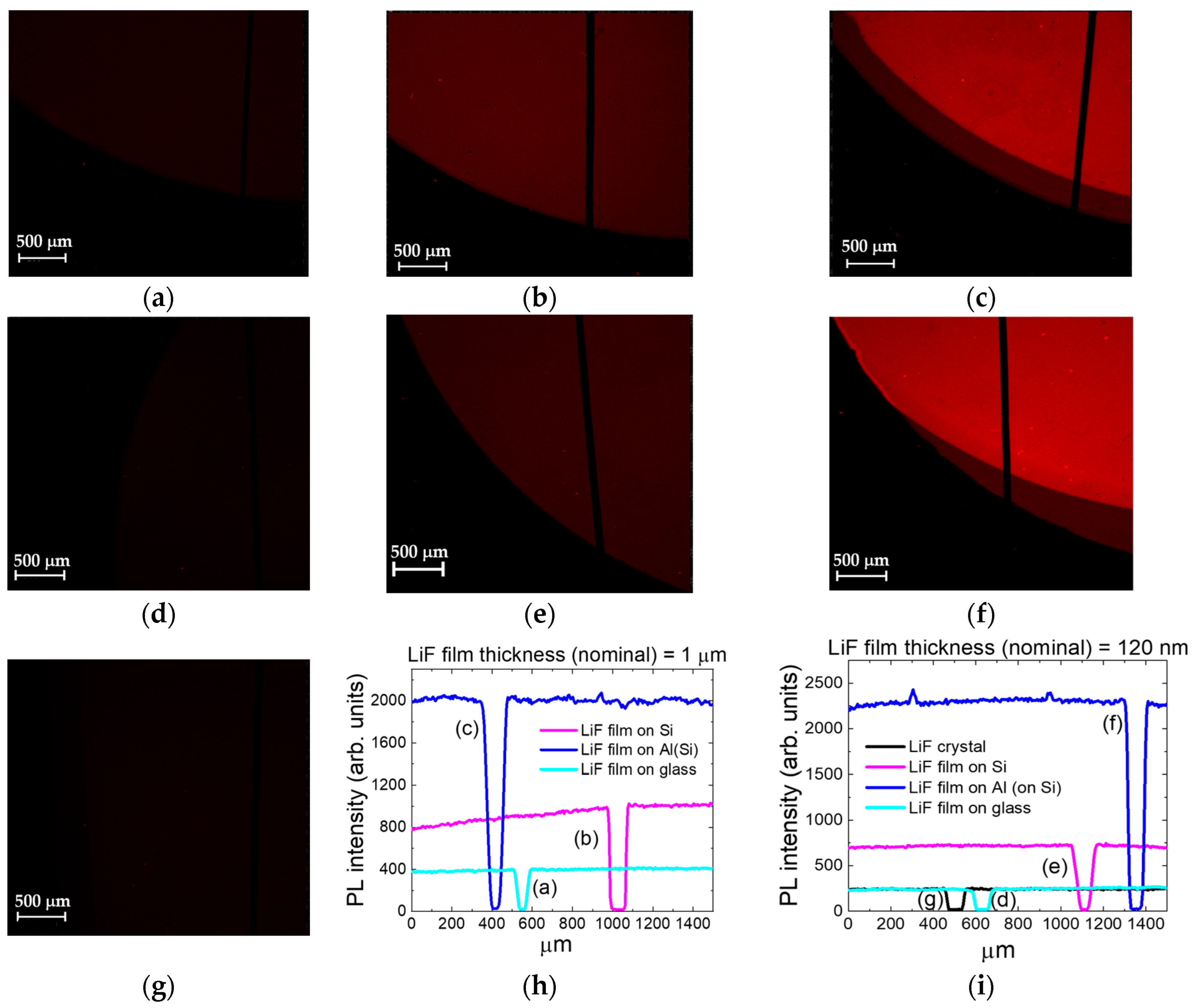
Figure 1a–c report the red PL signals of F2 CCs by CLSM images of LiF films with a nominal thickness of 1 μm grown on glass (a) Si(100) (b) and Si(100) coated with a thermally evaporated 200 nm-thick Al film (c) substrates and irradiated under the same conditions (X-ray fluence measured in the vacuum chamber = 20 μJ/cm2). Figure 1d–f report the CLSM images of LiF films with a nominal thickness of 120 nm grown on glass (d), Si(100) I, and Si(100) coated with a 200 nm-thick Al film (f) substrate and irradiated under the same conditions (X-ray fluence measured in the vacuum chamber = 70 μJ/cm2). Figure 1g reports the CLSM image of a LiF crystal (thickness 0.5 mm) irradiated under the same conditions of the 120 nm-thick LiF films reported in Figure 1d–f. The images show the edges of the round-shaped (diameter 1 cm) irradiated LiF films. The darker lines in the images are the shadows of a man’s hair placed in direct contact with LiF films during the X-ray irradiations as reference absorption contrast objects. The fluorescence images show that the PL intensity of the irradiated LiF film deposited on an Al-coated substrate is higher than that of LiF films grown on glass and Si substrates for both film thicknesses (see Figure 1h,i which shows the PL intensity profiles measured along a horizontal line of the corresponding CLSM images, including the hair shadow). Taking into account the reflectivity of the different substrates at the visible emission wavelengths of the radiation-induced CCs in LiF films, the main role of the substrates is evident, in this characterization, in the detected intensities of PL signals. Moreover, the CC PL signal of the LiF crystal (Figure 1g) is lower than that of the LiF films irradiated under the same conditions (Figure 1d–f). The formation efficiency of primary F centers and visible emitting F3+ and F2 aggregate defects is higher in polycrystalline LiF films than in single crystals and is influenced by the peculiar structure of the LiF films. It is generally accepted that the surface-to-volume ratios and the film compactness play a relevant role because they establish the density of the grain boundaries, which act as a source of vacancies during the color center formation and stabilization processes.
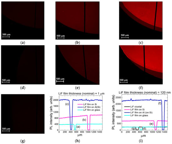
Figure 1.
(a–c) Fluorescence CLSM images of LiF films, with a nominal thickness of 1 μm, grown on glass, Si(100)and Al substrates irradiated with soft X-rays (fluence: 20 μJ/cm2); (d–f) fluorescence CLSM images of LiF films, with a nominal thickness of 120 nm, deposited on glass, Si(100) and Al substrates irradiated with soft X-rays (fluence: 70 μJ/cm2). (g) Fluorescence CLSM image of a LiF crystal (thickness 0.5 mm) irradiated with soft X-rays (fluence: 70 μJ/cm2). (h,i) PL intensity profiles measured along a line of the corresponding CLSM images including the hair shadow.
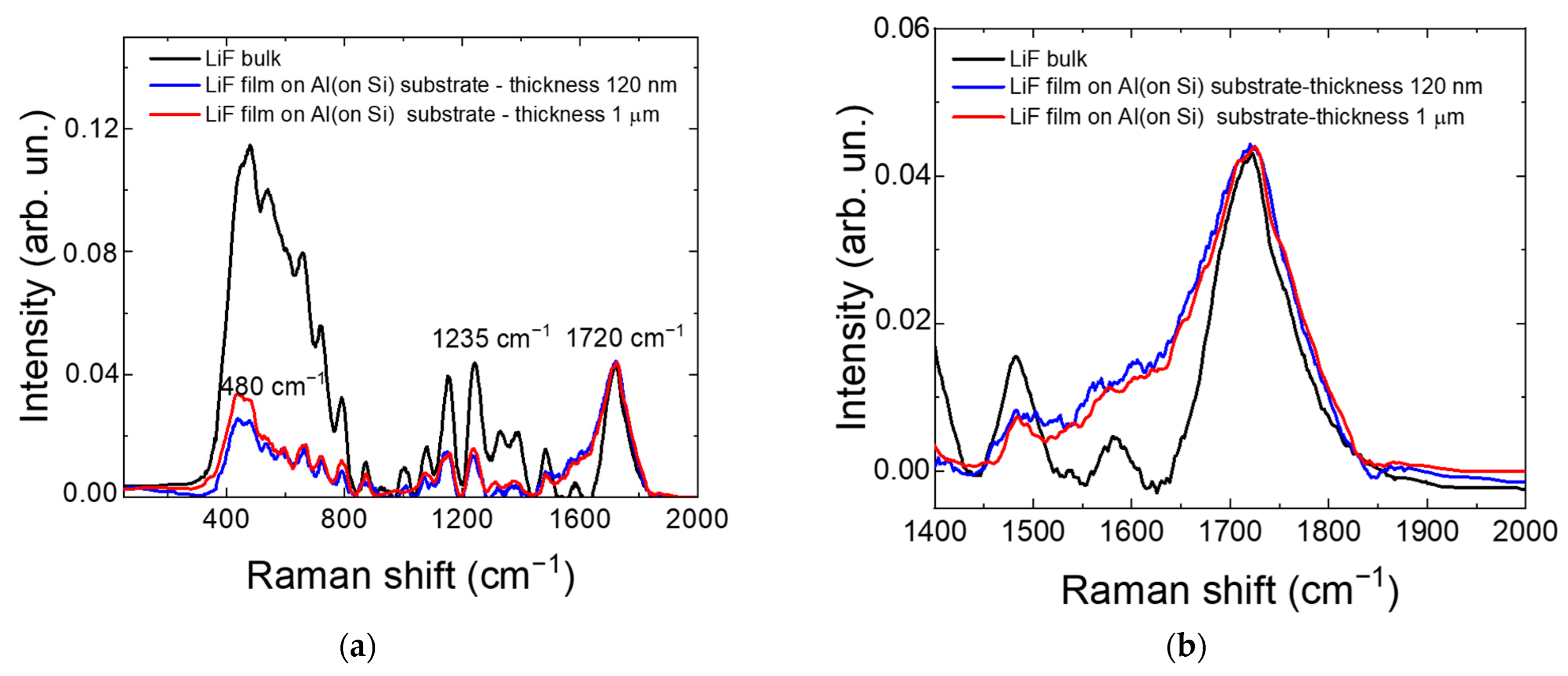
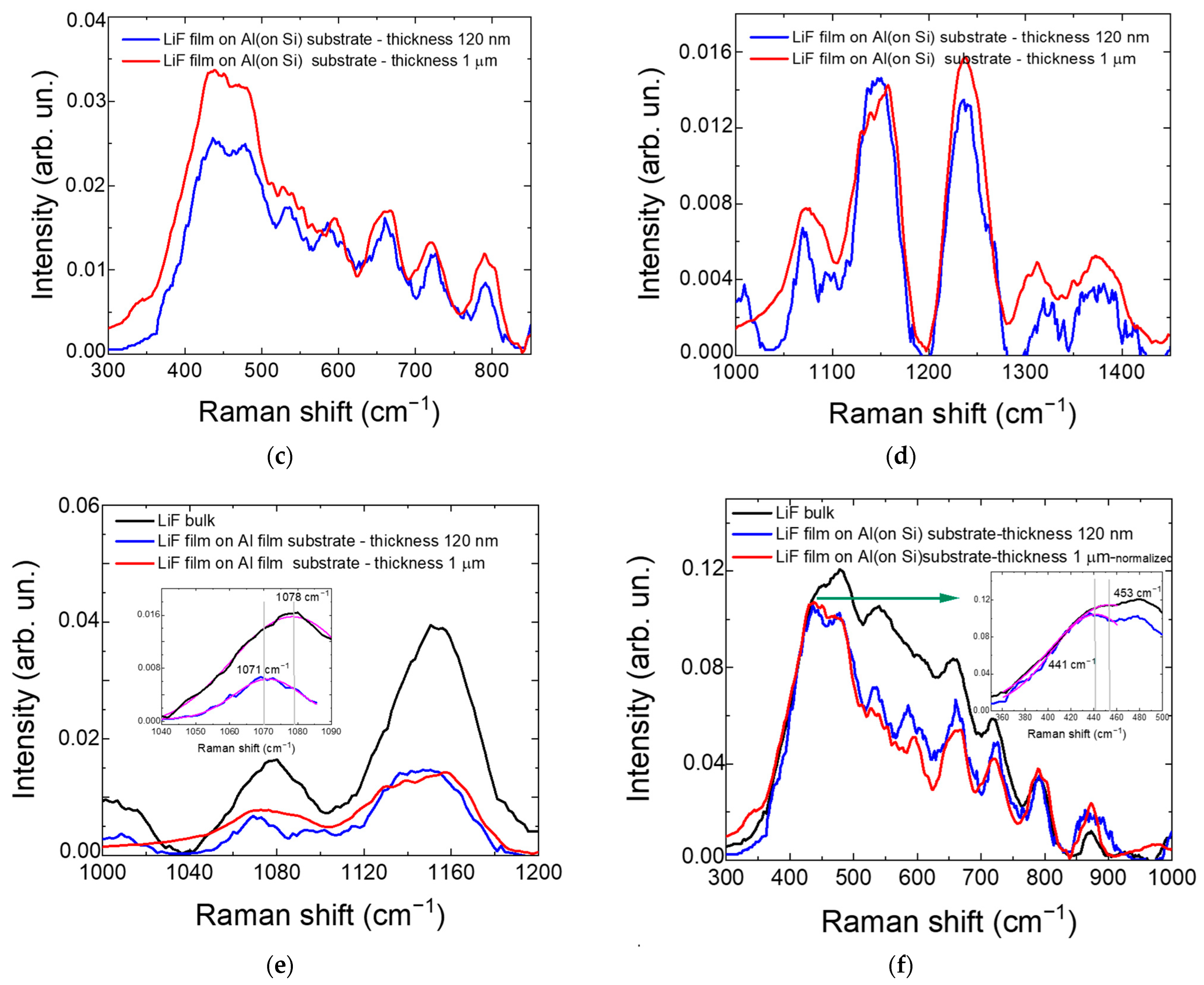
The role of the polycrystalline film structures in CC formation efficiency at the microscopic level is a fundamental aspect of the development of LiF film radiation-imaging detectors with the highest sensitivity. For this purpose, an investigation using Raman spectroscopy of the irradiated LiF films and crystal, combined with an Atomic Force Microscopy (AFM) characterization, was performed. Figure 2a compares the normalized Raman spectrum acquired in a point of the colored areas of the irradiated LiF crystal with that of the irradiated LiF films on the Al film-coated substrate with the two nominal thicknesses of 120 nm and 1 μm. Raman spectra were acquired with a 638 nm excitation wavelength. So called bunched Raman spectra, due to a large number of vibrational modes of alkali halides, were obtained [23]. In the Raman spectra reported in Figure 2, we observe peaks at 480 and 1235 cm−1, and their combination at 1720 cm−1. On the basis of the Raman peak identifications in [22], we can tentatively assign the 480 cm−1 peak to longitudinal optical modes and the 1235 cm−1 peak to surface optical modes. Figure 2b shows a zoomed in view of the Raman shift interval of spectra reported in Figure 2a and the broadening of the polycrystalline LiF film spectrum compared with the LiF crystal due to the higher degree of structural disorder in LiF films is evident. In fact, when the phonon coherence length within a system is reduced due to disorder, or due to the particle size limiting the phonon propagation beyond the particle boundaries, there could be changes in the phonon modes. These changes mainly include phonon mode broadening due to the reduced phonon lifetime; a shift in the phonon mode may also be expected if the bond strength is significantly affected [24]. Moreover, Figure 2c,d show the Raman spectra broadening of 120 nm-thick LiF films compared to 1 μm-thick LiF films (for two different Raman shift intervals) due to their different microscopic structures (a higher structure disorder for thinner films). Figure 2e,f show that the Raman spectrum of the 120 nm LiF film is shifted toward a higher wavenumber compared to that of the bulk LiF, most probably due to the compression structure experienced during film growth.

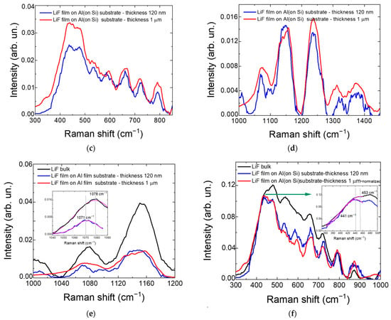
Figure 2.
(a) Normalized Raman spectra of the irradiated LiF crystal and LiF films (Al film-coated substrate with the two nominal thicknesses of 120 nm and 1 μm); (b–f) zoomed in view of (a) at different Raman shift intervals. The insets in the graphs (e,f) show a zoomed in view of the intervals 1040–1090 cm−1 and 350–500 cm−1, respectively, reporting fitting curves (in magenta color) for peak shift evaluations.
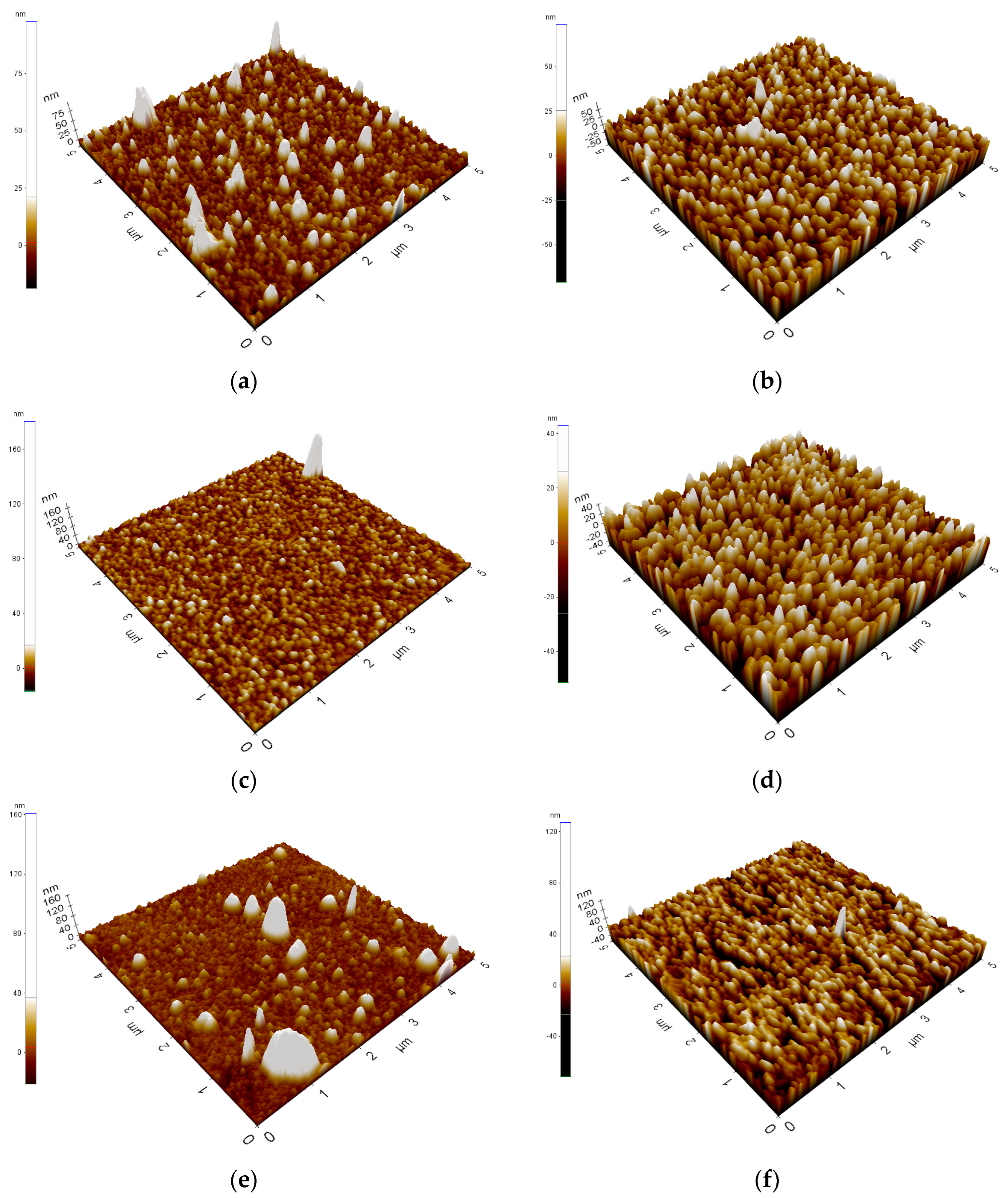
Figure 3 reports the AFM images of the LiF films grown on Al film-coated Si(100) substrates ((a), (b) with a nominal thickness of 120 nm and 1 µm, respectively); on Si(100) substrates ((c), (d) with a nominal thickness of 120 nm and 1 µm, respectively); on glass substrates ((e), (f) with a nominal thickness of 120 nm and 1 µm, respectively). The polycrystalline structures of the LiF films on the different substrates and for both two thickness are evident. Analyzing the AFM images reported in Figure 3, we obtained mean values of grain sizes and root mean square roughness (Rq) as reported in Table 1.
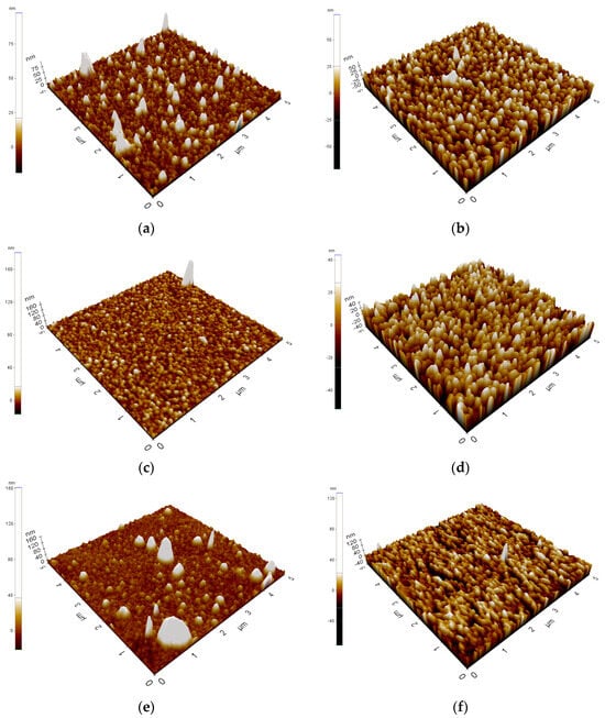
Figure 3.
The (5 × 5) μm2 AFM images of: (a) the 120 nm LiF film on Al; (b) the 1 µm LiF film on Al; (c) the 120 nm LiF film on Si; (d) the 1000 nm LiF film on Si; (e) the 120 nm LiF film on glass; (f) the 1 µm LiF film on glass.

Table 1.
Mean values of grain size and Rq of LiF films on Al film, Si, and glass substrates with two nominal thicknesses (120 nm and 1 µm).
The nature of the substrates and film thickness influence the microscopic structure of the LiF films grown by thermal evaporation. The AFM images show that thinner LiF films present smaller grain sizes than thicker films. Smaller grain dimensions result in higher degree of structural disorder and a larger number of vibrational modes, confirming the observation of the Raman spectra broadening of the thinner films.
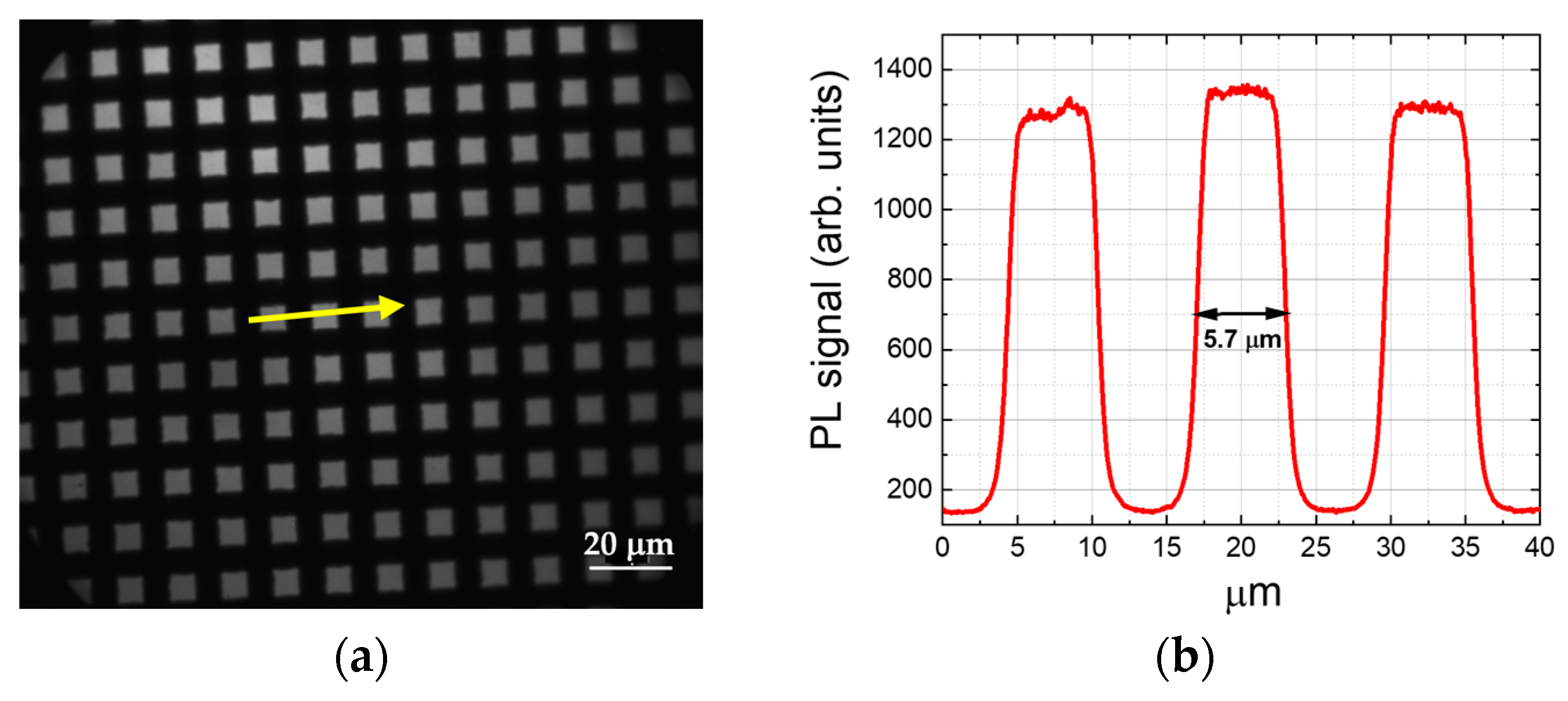
A LiF film (with a nominal thickness of 1 µm) on a Si(100) substrate was irradiated with soft X-rays by placing a metallic mesh (wire thickness of 5 μm) in direct contact with the LiF film surface. The X-ray image of the mesh stored in the LiF film was read by detecting the fluorescence image of the radiation-induced CCs and reported in Figure 4a. The images in Figure 4a show the PL intensity distribution arises from the locally patterned CCs produced during X-ray exposure. The black parts of the image represent the shadow of the mesh, while the grey parts represent the PL signal of CCs produced thorough the hole of the mesh. Figure 4b reports the fluorescence intensity profile along the yellow arrow of the image in Figure 4a.

Figure 4.
(a) Fluorescence image of the soft X-ray radiography of a metallic mesh stored in a LiF film (Si(100) substrate, with a nominal thickness of 1 µm). (b) Fluorescence intensity profile along the yellow arrow.
The combination of luminescence maps with Raman maps of the LiF film storing the soft X-ray image of the metallic mesh was performed with the confocal micro-spectrometer operating in the Raman and luminescence modes. The luminescence map (red false color) reported in Figure 5a was obtained by scanning the sample in a prefixed grid and detecting the CC luminescence band peak at approximately 680 nm by exciting with a 532 nm laser. In Figure 5a, the luminescence map of the X-ray image of the mesh stored in the LiF film is overlapped with the optical image obtained in white light. Also in this image, the black parts of the image represent the shadow of the mesh, while the red parts represent the PL signal of CCs produced thorough the hole of the mesh. Moreover, Raman maps are obtained by scanning the sample in a prefixed grid and detecting the Raman spectrum at each point. Figure 5b reports the Raman spectra of the 2D map detected in a region (mesh hole) with uncovered radiation-induced CCs and in the shadow of a mesh wire that covered the LiF during irradiation. In this graph, amplification of the active Raman modes due to the CCs produced in the mesh hole compared to the Raman spectrum detected in the shadow of a mesh wire is evident. Raman maps were visualized at different Raman shift intervals: 1190–1270 cm−1, where the peak at 1235 cm−1 is highlighted in Figure 2a (blue map of Figure 5c); 1450–1550 cm−1 (red map of Figure 5d); 1650–1750 cm−1 where the peak at 1720 cm−1 is highlighted in Figure 2a) (green map of Figure 5e). The black parts of the Raman maps represent the shadow of the mesh, as in the fluorescence images reported in Figure 4a and Figure 5a, while the colored parts represent the maps of the amplified Raman signal of LiF due to the presence of CCs produced thorough the hole of the mesh. This Raman 2D pattern should be overlapped to the combined luminescence maps reported in Figure 5a and to the fluorescence image reported in Figure 4a. Figure 5 clearly demonstrates that the presence of the defects in the hole of the mesh, as highlighted by the luminescence map (Figure 5a), destroys LiF lattice symmetry, enabling the observation of Raman spectra also at first order, as reported in the corresponding Raman maps in three different Raman shift intervals (Figure 5c–e), with different Raman peaks of the spectra reported in Figure 5b, detected a region with the presence of CCs.
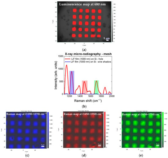
Figure 5.
The 2D Raman/luminescence maps obtained with the confocal micro-spectrometer of the X-ray image of the mesh stored in the LiF film (Si substrate, with a nominal thickness of 1 μm). (a) Luminescence map (red false color) overlapped with the optical image obtained in white light. (b) Raman spectra of the 2D map detected in a region (mesh hole) with uncovered radiation-induced CCs and in the shadow of a mesh wire that covers the LiF during irradiation. (c–e) Raman maps at different Raman shift intervals.
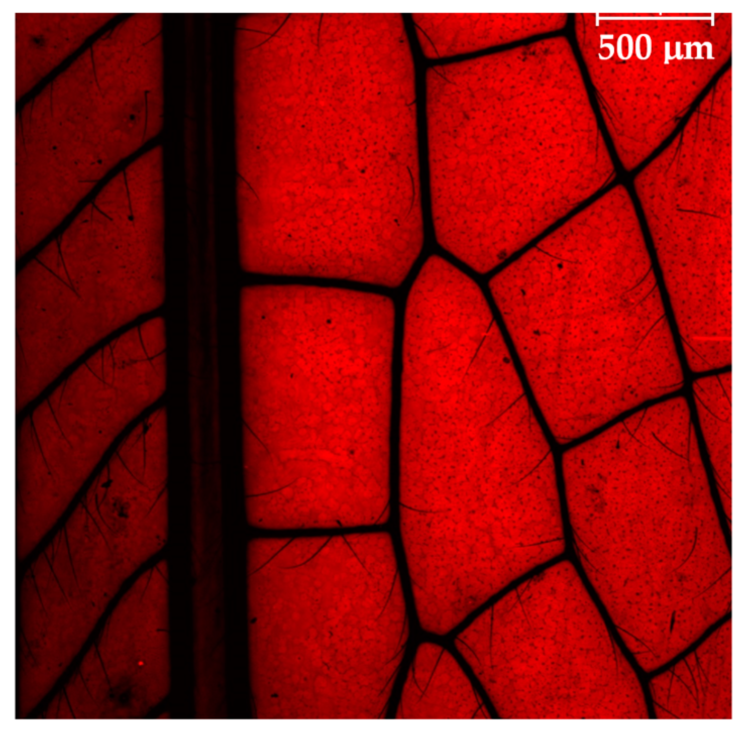
A LiF film (with a nominal thickness of 100 nm) on a Si(100) substrate was irradiated with soft X-rays by placing a dragonfly wing in direct contact with the LiF film surface. The X-ray image of the wing stored in the LiF film was read by detecting the fluorescence of the radiation-induced CCs with the confocal fluorescence microscope (Figure 6). The darker parts of the image represent the more absorbing part of the wing; and small details, such as ribs, hairs and texture are well distinguished, demonstrating the high spatial resolution and wide dynamic range of LiF films as soft X-ray imaging detectors.

Figure 6.
Fluorescence CLSM image of the soft X-ray radiography of a dragonfly wing stored in a LiF film (Si substrate, with a nominal thickness of 100 nm).
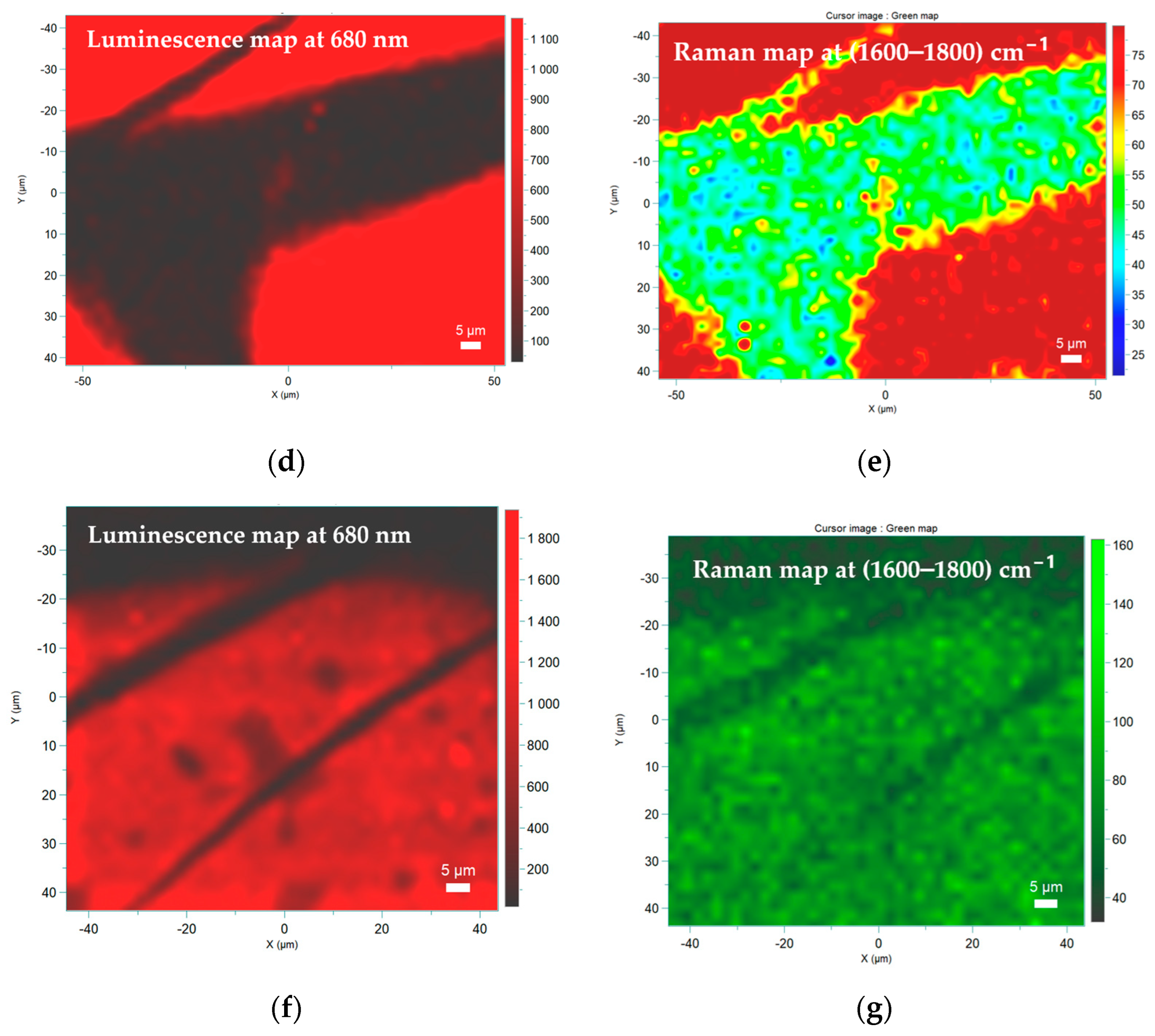
The combination of luminescence maps with Raman maps for a LiF film storing the soft X-ray image of the dragonfly wing was performed with the confocal micro-spectrometer operating in the Raman and luminescence modes. The luminescence maps (reported in red false color) in Figure 7a,b,d,f were obtained by scanning different areas at different magnifications and detecting the CC luminescence band peak at approximately 680 nm by exciting with a 532 nm laser. The black parts of the luminescence maps represent the more absorbing details of the wing (ribs and hairs), as in the fluorescence images reported in Figure 6. The corresponding Raman maps were visualized in the 1600–1800 cm−1 Raman shift interval, where the peak at 1720 cm−1 is highlighted in Figure 2a. The Raman maps show lower signals in more absorbing parts and confirm the lower presence of radiation-induced CCs responsible for Raman signal amplification.
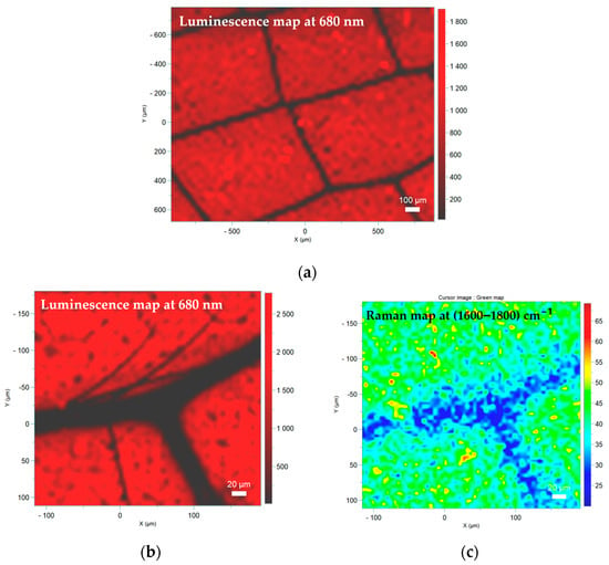
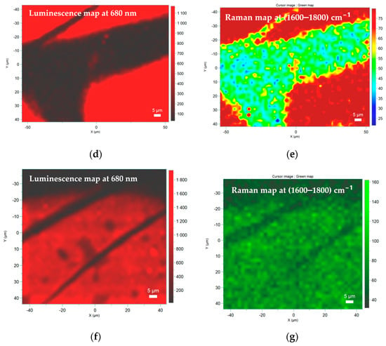
Figure 7.
The 2D Raman/luminescence maps obtained with the confocal micro-spectrometer of the soft X-ray radiography of a dragonfly wing stored in a LiF film (Si substrate, with a nominal thickness of 100 nm). (a,b,d,f) Luminescence maps obtained detecting the CC luminescence band peak at approximately 680 nm. (c,e,g) Raman maps were visualized in the 1600–1800 cm−1 Raman shift interval.
3. Discussions
LiF films grown by thermal evaporation on different substrates with two thicknesses of up to 1 μm were irradiated with soft X-rays produced by a laser plasma source. The irradiated LiF films were analyzed by fluorescence microscopy, AFM and Raman/luminescence micro-spectroscopy.
Fluorescence images of the irradiated LiF films show the role of substrate materials, in particular their reflective properties at the CC emission wavelengths, in the enhanced sensitivity of such X-ray detectors. LiF film radiation-imaging detectors assure great versatility, as they can be grown by thermal evaporation in the form of optically transparent thin films on different substrates on a wide range of thicknesses (several nm up to several microns) and dimensions (up to several cm2), tailoring the appropriate geometry. This versatility enables realizing vertical multilayer structures to increase the collection efficiency of the photoluminescence signal emitted by CCs and, consequently, the sensitivity of the detector. Moreover, fluorescence images of the irradiated LiF crystal compared with that of LiF films have demonstrated that CC formation efficiency is influenced by microscopic structures such as the surface-to-volume ratios, the film grain boundaries that should have a role in the color center formation and stabilization processes. These measurements demonstrate that the role of the polycrystalline film structures in CC formation efficiency at the microscopic level is a fundamental aspect of the development of LiF film radiation-imaging detectors.
For this purpose, advanced characterization of the irradiated LiF films and crystals by Raman micro-spectroscopy has been performed, obtaining results about the different structures at the microscopic level, mainly related to the degree of structural order.
Moreover, the combination of the Raman spectra of LiF films containing radiation-induced CCs and the corresponding AFM analysis has been performed. The nature of the substrate and the film thickness influence the microscopic structure of the LiF films grown by thermal evaporation, in particular grain size and root mean square roughness. The AFM images demonstrated that thinner LiF films present smaller grain sizes than thicker films. Smaller grain size shows a higher degree of structural disorder, confirming the observation of the Raman spectra broadening of the thinner films.
Regarding LiF film radiation-imaging detectors for X-ray micro-radiography, we demonstrated that Raman micro-spectroscopy, combined with the fluorescence microscopy represents a powerful tool to characterize X-ray micro-radiography for both the reference object (mesh) and biological samples (dragonfly wing). The combination of fluorescence images of CC patterns (standard technique to detect radiation-induced CCs) with the corresponding 2D Raman maps (advanced diagnostic technique for the study of the LiF film micro-structure) represents a very powerful tool to demonstrate that the presence of CCs destroying LiF lattice symmetry and amplifies the LiF Raman modes.
4. Materials and Methods
Optically transparent polycrystalline LiF thin films with two nominal thicknesses, 120 nm and 1 µm, were grown on different substrates (glass, Si(100), 200 nm-thick Al films grown on Si(100)) by thermal evaporation at ENEA C.R. Frascati, starting from LiF powder (Merck Suprapur, 99.99% pure). Before the deposition processes, glass and Si(100) substrates were cleaned by a procedure using detergents in ultrasonic baths. Substrates consisting of 200 nm-thick Al films deposited on Si(100) were grown by thermal evaporation starting from 99.999% pure aluminum wire heated in a tantalum crucible. The substrates were fixed onto a rotating sample holder inside the process steel vacuum chamber. The geometry of the sample holder enabled obtaining LiF film-based detectors with a circular radiation-sensitive area of diameter 10 mm. LiF powder, placed in a tantalum evaporation boat at the base of the vacuum chamber, 22 cm from the sample holder, was heated at a temperature of approximately 850 °C. Prior to the deposition processes, the pressure inside the vacuum chamber was below 1 mPa. During growth, the substrate temperature was maintained at 300 °C by using four halogen lamps controlled by a WEST N6400 controller, while an INFICON XTC/2 deposition controller, employing a quartz-crystal oscillator, was used for monitoring in situ the deposition rate, fixed at 1 nm/s, and LiF film thickness.
The LiF films were irradiated with a soft X-ray laser plasma source developed at Tor Vergata University [25] based on a Nd:YAG/Glass laser system (pulse duration = 15 ns, wavelength = 1064 nm) focused on a copper target in a vacuum chamber by a triplet lens on a spot with a diameter of approximately 300 μm on the surface of a stepped rotating solid tape target placed inside a vacuum chamber achieving a maximum intensity of approximately 1013 W/cm2 on the focal plane, sufficient to generate a hot and dense plasma. In our experiment, using a copper target, the plasma mainly emits spectral lines in the energy range from 0.05 eV to 2 keV (with most intense spectral lines in the range 1550–1580 eV). The energy of the X-rays emitted from the plasma was measured by a PIN photodiode with a 25 mm aluminum filter in order to evaluate the energy of X-rays with photon energies between 1 and 1.5 keV.
The LiF films with a nominal thickness of 1 µm grown on glass, Si(100) and Si(100) coated with a 200 nm-thick Al film substrate were irradiated under the same conditions, with the X-ray fluence measured in the vacuum chamber approximately 20 μJ/cm2. The LiF films with a nominal thickness of 120 nm grown on glass, Si(100) and Si(100) coated with a 200 nm-thick Al film substrate were irradiated under the same conditions, with the X-ray fluence measured in the vacuum chamber approximately 70 μJ/cm2. A commercially available, polished LiF crystal was also irradiated under the same conditions as reference.
The irradiated LiF films were read by detecting F2 and F3+ CC visible PL by means of a confocal laser scanning microscope operating in the fluorescence mode. In this microscopy apparatus (Nikon Eclipse 80i-C1), a continuous laser at 445 nm is used as the scanning illumination source to simultaneously excite F2 and F3+ CCs. In the fluorescence operating mode, the PL signals emitted by these CCs are detected by a system of two photomultipliers, which simultaneously and independently acquire two different spectral regions selected by appropriated optical filters.
The 2D Raman maps were measured by a Raman spectrometer combined with a confocal microscope (Horiba XploRA Plus) equipped with 532 and 638 nm wavelength lasers. When a Raman spectrometer is combined with a confocal optical microscope, it is possible to acquire the information of a complete Raman spectrum at each point of the 2D maps by scanning the sample in the XY directions. This confocal micro-spectrometer can also operate in the luminescence mode, enabling coupling Raman and luminescence maps.
Surface analysis was performed using a Park Systems XE-150 Atomic Force Microscope (AFM) operating in the non-contact mode. A pre-mounted non-contact high-resolution cantilever working at 304 MHz with a nominal tip radius below 10 nm was used.
5. Conclusions
Advanced characterization of LiF film-based X-ray detectors through the combination of fluorescence microscopy, Raman micro-spectroscopy and AFM measurements was performed. The obtained results have demonstrated that fluorescence/Raman spectral imaging and AFM maps could represent an advanced method to investigate the role of the polycrystalline film structures in CC formation efficiency at the microscopic level, a fundamental aspect of the development of LiF film radiation-imaging detectors. The obtained results provide the basis for further investigations to study the role of LiF film micro-structures (such as grain size, roughness, compactness, and degree of structural disorder) in CC formation efficiency.
Author Contributions
Conceptualization, F.B. and S.B.; methodology, F.B., S.B. and M.A.V.; formal analysis, S.B. and F.B.; investigation, F.B., S.B., M.A.V., R.M.M., A.R., P.G. and R.R.; writing—original draft preparation, F.B.; writing—review and editing, S.B., R.M.M., M.A.V., A.R., P.G. and R.R.; project administration, R.M.M.; funding acquisition, R.M.M. All authors have read and agreed to the published version of the manuscript.
Funding
Part of this research was funded by the TECHEA (Technologies for Health) Project and the Italian National Agency for New Technologies, Energy and Sustainable Economic Development (ENEA), Italy.
Data Availability Statement
Data are contained within the article.
Conflicts of Interest
The authors declare no conflict of interest.
References
- Sthoneham, A.M. Theory of Defects in Solids; Oxford University Press: Oxford, UK, 1975. [Google Scholar]
- Fowler, W.B. Physics of Color Centers; Academic Press: New York, NY, USA; London, UK, 1968. [Google Scholar]
- Shionoya, S.; Yen, W.M. Phosphor Handbook; CRC Press: Boca Raton, FL, USA, 1998. [Google Scholar]
- Yukihara, E.G.; McKeever, S.W.S. Optically Stimulated Luminescence: Fundamentals and Applications; Wiley: Hoboken, NJ, USA, 2011. [Google Scholar]
- Schulman, J.H.; Compton, W.D. Color Centers in Solids; Smoluchowski, R., Kurti, N., Eds.; Pergamon Press: Oxford, UK, 1963. [Google Scholar]
- Lakshmanan, A.R.; Madhusoodanan, U.; Natarajan, A.; Panigrahi, B.S. Photoluminescence of F-aggregate centers in thermal neutron irradiated LiF TLD-100 single crystals. Phys. Stat. Sol. 1996, 153, 265–273. [Google Scholar] [CrossRef]
- Montereali, R.M.; Bonfigli, F.; Vincenti, M.A.; Nichelatti, E. Versatile lithium fluoride thin-film solid-state detectors for nanoscale radiation imaging. Il Nuovo C 2013, 36 C, 35–42. [Google Scholar] [CrossRef]
- Calegari, F.; Valentini, G.; Vozzi, C.; Benedetti, E.; Cabanillas-Gonzalez, J.; Faenov, A.; Gasilov, S.; Pikuz, T.; Poletto, L.; Sansone, G.; et al. Elemental sensitivity in soft x-ray imaging with a laser-plasma source and a color center detector. Opt. Lett. 2007, 32, 2593–2595. [Google Scholar]
- Gasilov, S.V.; Faenov, A.Y.; Pikuz, T.A.; Skobelev, I.Y.; Calegari, F.; Vozzi, C.; Nisoli, M.; Sansone, G.; Valentini, G.; De Silvestri, S.; et al. Phase-contrast imaging of nanostructures by soft x rays from a femtosecond-laser plasma. JETP Lett. 2008, 87, 238–242. [Google Scholar] [CrossRef]
- Kurobori, T.; Matoba, A. Development of accurate two-dimensional dose-imaging detectors using atomic-scale color centers in Ag-activated phosphate glass and LiF thin films. Jpn. J. Appl. Phys. 2014, 53, 02BD14. [Google Scholar] [CrossRef]
- Barkusky, F.; Peth, C.; Mann, K.; Feigel, T.; Kaiser, N. Formation and direct writing of color centers in LiF using a laser-induced extreme ultraviolet plasma in combination with a Schwarzschild objective. Rev. Sci. Instrum. 2005, 76, 105102. [Google Scholar] [CrossRef]
- Bonfigli, F.; Capotondi, F.; Cricenti, A.; Giannessi, L.; Kiskinova, M.; Luce, M.; Mahne, N.; Manfredda, M.; Montereali, R.M.; Nichelatti, E.; et al. Imaging detectors based on photoluminescence of radiation-induced defects in lithium fluoride for XFEL beam monitoring. Il Nuovo C 2019, 42 C, 237. [Google Scholar] [CrossRef]
- Pikuz, T.; Faenov, A.; Matsuoka, T.; Matsuyama, S.; Yamauchi, K.; Ozaki, N.; Albertazzi, B.; Inubushi, Y.; Yabashi, M.; Tono, K.; et al. 3D visualization of XFEL beam focusing properties using LiF crystal X-ray detector. Sci. Rep. 2015, 5, 17713. [Google Scholar] [CrossRef] [PubMed]
- Pikuz, T.; Faenov, A.; Fukuda, Y.; Kando, M.; Bolton, P.; Mitrofanov, A.; Vinogradov, A.; Nagasono, M.; Ohashi, H.; Yabashi, M.; et al. Optical features of a LiF crystal soft x-ray imaging detector irradiated by free electron laser pulses. Opt. Express 2012, 20, 3424–3433. [Google Scholar] [CrossRef]
- Bilski, P.; Marczewska, B.; Gieszczyk, W.; Kłosowski, M.; Nowak, T.; Naruszewicz, M. Lithium fluoride crystals as fluorescent nuclear track detectors. Radiat. Prot. Dosim. 2018, 178, 337–340. [Google Scholar] [CrossRef] [PubMed]
- Bilski, P.; Marczewska, B. Fluorescent detection of single tracks of alpha particles using lithium fluoride crystals. Nucl. Instrum. Methods Phys. Res. Sect. B Beam Interact. Mater. At. 2017, 392, 41–45. [Google Scholar] [CrossRef]
- Cosset, F.; Celerier, A.; Barelaud, B.; Vareille, J.C. Thin reactive LiF films for nuclear sensors. Thin Solid Film. 1997, 303, 191–195. [Google Scholar] [CrossRef]
- Nahum, J.; Wiegand, D.A. Optical Properties of Some F-Aggregate Centers in LiF. Phys. Rev. 1967, 154, 817–830. [Google Scholar] [CrossRef]
- Yadav, R.P.; Dwivedi, S.; Mittal, A.K.; Kumar, M.; Pandey, A.C. Analyzing the LiF thin films deposited at different substrate temperatures using multifractal technique. Thin Solid Film. 2014, 562, 126–131. [Google Scholar] [CrossRef]
- Nichelatti, E.; Almaviva, S.; Bonfigli, F.; Franzini, I.; Montereali, R.M.; Vincenti, M.A. Photoluminescence from colour centres generated in lithium fluoride thin films and crystals by extreme-ultraviolet irradiatio. Nucl. Instrum. Methods Phys. Res. B 2010, 268, 3035–3039. [Google Scholar] [CrossRef]
- Sekatskii, S.K.; Letokhov, V.S. Single fluorescence centers on the tips of crystal needles: First observation and prospects for application in scanning one-atom fluorescence microscopy. Appl. Phys. B 1996, 63, 525–530. [Google Scholar] [CrossRef]
- Liu, F.; Wang, G.; Cheng, G. Raman scattering from fractal structure of LiF nanocluster-assembled films. J. Phys. Chem. Solids 1996, 57, 507–512. [Google Scholar] [CrossRef]
- Krishnan, R.S.; Narayanan, P.S. The vibration spectra of the alkali halides. Proc. Ind. Acad. Sci. A 1948, 28, 296–306. [Google Scholar] [CrossRef]
- Rambadey, O.V.; Gupta, M.; Kumar, A.; Sagdeo, P.R. Analysis of structural disorder on Raman spectra of semiconductors. J. Appl. Phys. 2023, 133, 131101. [Google Scholar] [CrossRef]
- Martellucci, S.; Bellecci, C.; Francucci, M.; Gaudio, P.; Richetta, M.; Toscano, D.; Rydzy, A.; Gelfusa, M.; Ciuffa, P. Soft X-ray generation by a tabletop Nd:YAG/glass laser system. J. Phys. Condens. Matter 2006, 18, S2039. [Google Scholar] [CrossRef]
Disclaimer/Publisher’s Note: The statements, opinions and data contained in all publications are solely those of the individual author(s) and contributor(s) and not of MDPI and/or the editor(s). MDPI and/or the editor(s) disclaim responsibility for any injury to people or property resulting from any ideas, methods, instructions or products referred to in the content. |
© 2023 by the authors. Licensee MDPI, Basel, Switzerland. This article is an open access article distributed under the terms and conditions of the Creative Commons Attribution (CC BY) license (https://creativecommons.org/licenses/by/4.0/).

