Article

Towards the Construction of an Analog Solver for the Schrödinger and Ginzburg–Landau Equations Based on a Transmission Line

by
Krzysztof Pomorski
1,2,*,
Łukasz Pluszyński
2,3 and
Eryk Hałubek
1,2
1
Institute of Physics, Lodz University of Technology, 90-924 Lodz, Poland
2
Quantum Hardware Systems, 94-056 Lodz, Poland
3
Faculty of Electrical and Electronic Engineering, Cracow University of Technology, 31-155 Cracow, Poland
*
Author to whom correspondence should be addressed.
Condens. Matter 2024, 9(4), 35; https://doi.org/10.3390/condmat9040035
Submission received: 14 May 2024 / Revised: 19 July 2024 / Accepted: 30 August 2024 / Published: 26 September 2024

Abstract

:
The model presented by Gabriel Kron in 1945 is an example of an analog computer simulating quantum phenomena on a hardware level. It uses passive RLC elements to construct a hardware solver for the problem of quantum particles confined by rectangular or other classes of potential. The analytical and numerical validation of Kron’s second model is conducted for different shapes of particle-confining potentials in the one-dimensional case using an LTspice simulator. Thus, there remains potential for obtaining solutions in two- and three-dimensional cases. Here, a circuit model representing a linearized Ginzburg–Landau equation is given. Kron’s second model is generalized by the introduction of linear and non-linear resistive elements. This transforms the deformed Schrödinger equation into a linear dissipative Schrödinger equation and its non-linear form. The quantum mechanical roton problem is the main result of this work and is formulated by means of classical physical states naturally present in the LC classical circular electrical transmission line. The experimental verification of Kron’s model is confirmed.

1. Introduction

1.1. Motivation behind the Development of Analog Computer Modeling Quantum Systems

Analog computers are a class of computers that operate on continuous signals, instead of discrete numbers like most commonly used binary-based digital electronics. The greatest strength of the analog paradigm is its ability to utilize the known physical relationships between their components to solve computationally difficult equations as integro-differential equations [1], without the need for the technically costly approximation of real numbers by discrete states, or for differentiation and integration operators. One of the most commonly known examples is the use of the relationship between the input and output voltages of an operational amplifier with a correctly placed capacitor to obtain the integrals or derivatives of the function of the electrical signal.
Analog electronics are able to represent various differential equations related to a wide class of problems. However, this potential is underutilized due to the difficulty of integrating analog electronics with digital systems. Analog systems tend to cause interference. Another recurring problem is the occurrence of effectively built-in parasitic resistances.
Quantum mechanics incorporates massive parallelism, expressed by the superposition principle and non-local correlations described by Dirac, Fitzpatrick, Binney, and Skinner [2,3,4]. Thus, quantum mechanics marks a break from classical physics, introducing a new paradigm for information processing. Currently, quantum electronics and quantum algorithms are attracting much research interest. In particular, quantum chemistry is under rapid development, as indicated by the IBM Quantum Experience or Motta and Rice [5], which is also resulting in the development of new algorithms [6]. Here, we present a classical hardware implementable analog solver for the Schrödinger equation based on Kron’s second model [7,8]. We demonstrate its generalization via numerical validation for classes of effective potential beyond rectangular potential. The presented work goes beyond the analog electronic circuits presented by [5,9] as it discusses the quantum roton problem and opens the perspective of finding solutions for various families of non-linear Schrödinger equations. It is, thus, aligned with designing a hybrid digital/analog quantum physics emulator [10] or the emulation of quantum algorithms using various forms of classical analog electronics [11].

1.2. Summary of the State of the Art in the RLC Circuit Design Simulating Quantum Mechanics

Any isolated quantum system can be described by the following equation of motion [2].
i d d t | ψ ( t ) = H ^ ( t ) | ψ ( t ) ,
where | ψ ( t ) is a finite or infinite quantum state vector and H ^ is a finite- or infinite-dimensional square matrix. In the case of weak environment interaction with a given quantum system, the effective Hamiltonian will change from Hermitian into the non-Hermitian form, and thus, the eigenenergies will have complex values, so the normalization of a quantum state is no longer preserved. Due to technical limitations in terms of computation capability and memory capacity, we limit ourselves to a finite size of the Hilbert space, which is either the full description of reality or might be the first level of approximation of the QM system dynamics with the use of a truncated (reduced) Hilbert space [12].
Currently, we are able to simulate the following classes of quantum systems:
  • Linear diffusion equation known as the Schrödinger equation [7].
  • Non-Linear diffusion equation known as the Schrödinger equation and its various versions as the Gross–Pitaevskii equation [13].
  • Quantum Spin of particle(s) [14].
  • Josephson junction networks [12].
  • Quantum chips [15].
Initially, the research was centered on further extensions of Kron’s original models [7], which are based on an RLC circuit simulating dissipative or non-dissipative quantum mechanics. It is, for example, focused on the development of circuits modeling trapped Bose–Einstein condensates [13] or the expansion of Kron’s model toward two or three dimensions [8]. Previous research efforts have been focused on the derivation of non-linear equations, resulting in the explicit introduction of resistors generating a hypothetical Schrödinger potential component with imaginary values [16] or the Schrödinger–Hertz equation [8] and Gross–Pitaevskii equation [8]. A full review of non-linear Schrödinger equation models is available in [17]. Central to these models, there is the mechanism of creating non-linearities based on an n–p semiconductor junction polarized by static voltage in the reverse direction, thus accounting for voltage controllable capacitance, or on the use of the field effect transistors. According to the literature, topological insulating and semi-metallic states can be realized in a periodic RLC circuit [18]. Furthermore, new possibilities are opened by the implementation of fractional derivatives in analog electronic circuits, which could lead to a fractional Schrödinger equation. It is of key importance that the LC circuits in a long line can be described by Hamiltonians or Lagrangians and, subsequently, perturbed by dissipative elements, such as resistors or non-linear resistors used as diodes in various configurations.
The presented work encompasses the following sections: (1) the already given State of the Art with analog electronics simulating Schrödinger-like equations; (2) the derivation of Kron’s second model; (3) the numerical LTspice simulations of Kron’s second circuit; (4) the LC circuits representing the linearized Ginzburg–Landau equation; (5) the conclusions with acknowledgments and references.

2. Kron’s Second Model of the Analog Hardware Solver for the Schrödinger Equation

As established by Gabriel Kron [7], the distribution of a one-dimensional wave function of the Schrödinger equation can be represented for a single particle in effective potential by a classical non-uniform transmission line using inductive and capacitive elements only. Indeed, Kron’s second model utilizes a model of a classical transmission line with the driving signal (a voltage source or current source) of constant frequency and amplitude. In this model, we have inductance in the horizontal direction, while we set capacitance and inductance in a parallel configuration in the vertical direction, as depicted in Figure 1 and Figure 2. Kron’s model uses a simplistic Hamiltonian of the Schrödinger equation ( H ^ ( x ) E ) ψ ( x ) = 0 , which can be represented in discrete form as
Δ x H ^ ( x ) ψ ( x ) Δ x E ( t ) ψ ( x ) = 0 , H ^ ( x ) = T ^ ( x ) + V ^ ( x ) , 2 2 m ( ψ ( x + Δ x ) ψ ( x ) ) = Δ x ( E V p ( x ) ) ψ ( x ) , I ^ ( x + Δ x , t ) I ^ ( x , t ) = Δ I ^ ( x , t ) = V ^ ( x ) Z ( x ) C 1 | | L 1 = ( j C 1 ω + 1 j ω L 1 ( x ) ) V ^ ( x ) = Δ x ( E V p ( x ) ) ,
with the central a priori assumption that kinetic energy in the Schrödinger equation corresponds to the electric current phasor changing to I ^ ( x + Δ x , t ) I ^ ( x , t ) , which leads to the current phasor Δ I ^ ( x ) flowing vertically through every lattice step Δ x in the form
2 2 m ( ψ ( x + Δ x ) ψ ( x ) ) = I ^ ( x + Δ x , t ) I ^ ( x , t ) = Δ I ^ ( x , t ) ,
which implies
( I ^ ( x + Δ x , t ) I ^ ( x , t ) ) = Δ I ( x , t ) = V ^ ( x ) Z ( x ) C 1 | | L 1 = ( j C 1 ω + 1 j ω L 1 ( x ) ) V ^ ( x ) = Δ x ( E V p ( x ) ) ,
and under the assumption ψ ( x ) = V ^ ( x ) , we arrive at the dependence
2 2 m ( V ^ ( x + Δ x ) V ^ ( x ) ) = Δ I ^ ( x ) , ( d d x V ^ ) = 2 m 2 Δ I ^ ( x ) Δ x = Δ Z L ( x ) Δ x I ^ ( x ) = j L ω I ^ ( x ) ,
where V ^ p is the potential energy operator, T ^ is the kinetic energy operator equal to 2 2 m d 2 d x 2 or p 2 2 m , H ^ is the Hamiltonian equivalent to V ^ + T ^ , E is the energy eigenvalue, p ^ is a momentum operator equivalent to i d d x , and Δ x represents a discrete step in coordinates, while I ^ ( x ) and V ^ ( x ) are the phasors of the electric current and voltage. We have made the explicit assumption that the phasor of the voltage across the upper and lower branch represents the wave function. Furthermore, in the case of the transmission line mimicking the Schrödinger equation, as described by [2,3,4], we shall assume that 1 L 1 ( x ) = V p ( x ) Δ x and that C 1 ω 2 Δ x = E . Assuming the applicability of the concept of impedance, we observe that the horizontal inductance impedance X L = 2 m 2 Δ x is related to the kinetic energy operator, the vertical inductance X L 1 = 1 V Δ x is the inverse of potential energy, and the impedance of the capacitor X C = 1 E Δ x stands for the total energy. Such results are obtained by the derivation of Kron’s model, as described in Section 4. The basic representation of the energy operators in one dimension for the time-independent Schrödinger equation in Kron’s second model uses serial coils in the horizontal direction to represent the kinetic energy operator, inductive coils perpendicular to them to represent the potential energy operator, and capacitors connected parallelly to the vertical inductors to represent the total energy operator E, as depicted in Figure 2.
Figure 1 depicts Kron’s representations of particle movement in free space or with uniform potential, while Figure 2 depicts Kron’s representations of the Hamiltonian operator (a) and H E operator (b) for a particle moving in one dimension, represented by a classical electric circuit.
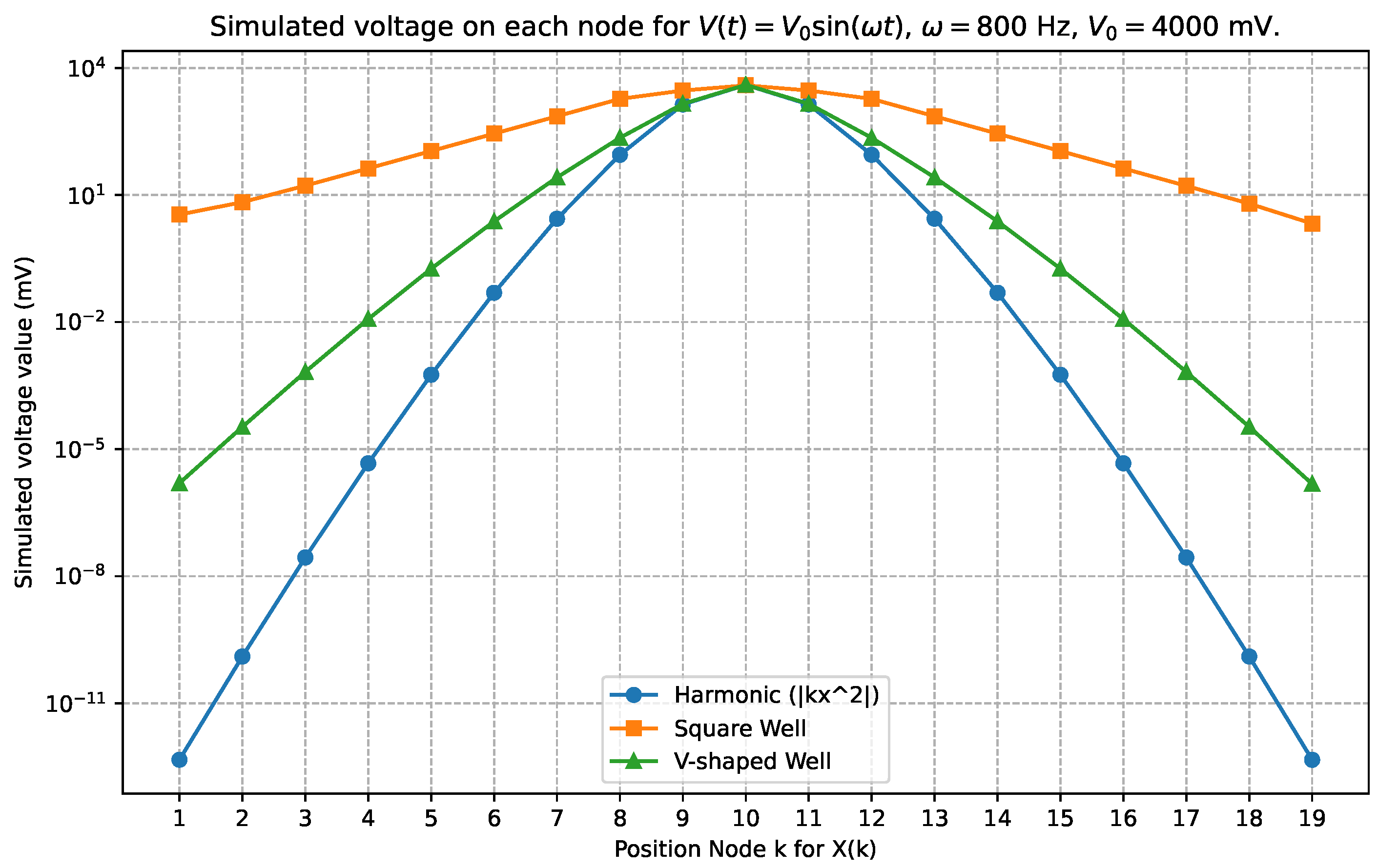
For the purposes of the simulation reflected in the analog hardware configuration, the location of the voltage signal generator will be the point of the lowest potential energy. In this case, it will be represented either by the node with the highest parallel inductance or the node without a parallel coil. This setup for a basic simulation of a particle in a rectangular well of potential is depicted in Figure 3.
Figure 3. Schemes of classical RLC circuits with 25 nodes for the simulation of a quantum particle [2] in a rectangular potential well (upper case), a “V”-shaped potential (middle case), and a harmonic potential well (lower case). All the simulations were run with the gear integration method, and an alternate solver was set as the simulation parameters in the LTspice freeware with the values specified in Table 1. The results obtained for low frequencies are depicted in Figure 4.
Condensedmatter 09 00035 g003
Figure 4. Obtained simulation results for the particle trapped in a rectangular, harmonic, and V s h a p e d potential well with the use of Kron’s second model implemented in the LTspice environment; the frequency of the signal generator is set to ω = 800 Hz with the parameters of the simulation set in Table 1.
Condensedmatter 09 00035 g004
Table 1. Simulation parameters for a square, V-shaped, and harmonic potential and renormalized values for a V-shaped potential are given in Table 2.
ParameterValue
Simulated Physical Time22 s, 24,120 s, 36,120 s
Time To Start Saving Data20 s, 24,000 s, 36,000 s,
Maximal Time Step0.00001 s, 0.00001 s, 0.00001 s,
Δ x1, 1, 1
Driving Signal FunctionSine, Sine, Sine,
Driving Signal Amplitude4 V, 4 V, 4 V
Driving Signal Frequency10 Hz, 2 Hz, 2 Hz
Position Index Of Node With Signal Generator13, 13, 13
Capacitance (Same For All Nodes)1 μ F, 1 μ F, 1 μ F
Inductance For Sequential Coils1 mH, 1 H, 1 H
Inductances For Coils (1–9, 17–25): Square Pot1 mH
Inductances For Coils (10 To 16) With Square PotNaN; Coils Removed
Inductances For Coils (13) In V Or HarmonicNaN; Coils Removed
Inductances For Coils (1, 25) In V Or Harmonic2 H, 0.00694 H
Inductances For Coils (2, 24) In V Or Harmonic4 H, 0.008264 H
Inductances For Coils (3, 23) In V Or Harmonic6 H, 0.01 H
Inductances For Coils (4, 22) In V Or Harmonic8 H, 0.012346 H
Inductances For Coils (5, 21) In V Or Harmonic10 H, 0.015625 H
Inductances For Coils (6, 20) In V Or Harmonic12 H, 0.0204082 H
Inductances For Coils (7, 19) In V Or Harmonic14 H, 0.0278 H
Inductances For Coils (8, 18) In V Or Harmonic16 H, 0.04 H
Inductances For Coils (9, 17) In V Or Harmonic18 H, 0.0625 H
Inductances For Coils (10, 16) In V Or Harmonic20 H, 0.111 H
Inductances For Coils (11, 15) In V Or Harmonic22 H, 0.25 H
Inductances For Coils (12–14) In V, Harmonic24 H, 1 H
Table 2. Proposed simulation parameters for a V-shaped potential well before and after renormalization by the k coefficient, so c o n s t 1 = L r e n ( x ) = k × L ( x ) = c o n s t 2 , L 1 , r e n ( x ) = k × L 1 ( x ) , C 1 = C 1 , r e n = c o n s t 3 , ω r e n = ω k , k = [ k 1 = 1 / 24 , 000 = 0.417 × 10 4 , 10 2 k 1 = k 2 = 1 / 2 , 400 , 000 = 0.417 × 10 6 ].
Parameter of V-ShapedValueRenormalized Value 1/Renormalized Value 2
Driving Signal Frequency2 Hz308.838 Hz/ 3098 Hz
Position Index Of Node With Signal Generator1313
Capacitance (All Nodes)1 μ F1 μ F
Inductance For Seq. Coils1 H0.0417 mH/0.417 μ H
Inductances For Coils (1, 25)2 H0.0833 mH/0.833 μ H
Inductances For Coils (2, 24)4 H0.167 mH/1.67 μ H
Inductances For Coils (3, 23)6 H0.25 mH/2.5 μ H
Inductances For Coils (4, 22)8 H0.34 mH/3.4 μ H
Inductances For Coils (5, 21)10 H0.417 mH /4.17 μ H
Inductances For Coils (6, 20)12 H0.5 mH/5 μ H
Inductances For Coils (7, 19)14 H0.583 mH/5.83 μ H
Inductances For Coils (8, 18)16 H0.67 mH/6.7 μ H
Inductances For Coils (9, 17)18 H0.75 mH/7.55 μ H
Inductances For Coils (10, 16)20 H0.833 mH/8.33 μ H
Inductances For Coils (11, 15)22 H0.91 mH/9.1 μ H
Inductances For Coils (12, 14)24 H1 mH/10 μ H
Inductances For Coil With Index 13NaN; Coil RemovedNaN; Coil Removed
The wave functions ψ for the Hamiltonian eigenstate we are looking for can only be electrically measured in an invasive way, as the potential difference between the nodes of the upper and lower branches of a transmission line. Due to the relationship between the electronic components, the circuit solves the equation only when the current running through the function generator driving the voltage signal equals zero [7].
It is worth noting that we can transit from the Schrödinger equation to the Ginzburg–Landau equation (as in the framework of the given numerical method or modification of operational hardware):
2 2 m d 2 d x 2 ψ ( x ) + V p ( x ) ψ ( x ) = E ψ ( x ) , 2 2 m d 2 d x 2 ψ ( x ) + α ( x ) ψ ( x ) + β ( x ) | ψ ( x ) | 2 ψ ( x ) = 0 ,
by assuming a priori the transition V p ( x ) ( α ( x ) + β ( x ) | ψ ( x ) | 2 + E ) (or with additional higher order polynomial terms based on the powers of the | ψ ( x ) | 2 variable). We obtain a transition from the Schrödinger to Ginzburg–Landau-like (a class of non-linear Schrödinger) equation(s). Alternatively, we can assume the a priori transition E ( V p ( x ) α ( x ) β ( x ) | ψ ( x ) | 2 ) (or with higher powers of | ψ ( x ) | 2 ) as implementing the transition from a Schrödinger equation to a non-linear Schrödinger equation [19]. Both transitions can be encoded in a certain dependence of L 1 and C 1 linear density, with certain space dependence and certain voltage dependence. The transition from the Schrödinger to Ginzburg–Landau formalism can mean a transition from a semiconductor to a superconductor. Symmetrized diodes (two diodes connected in an antiparallel way) are good candidates for circuit elements implementing a given transition (Schrödinger to GL), as a way of inducing non-linearity to the circuit. Furthermore, one can introduce three non-linear elements in the vertical direction, resistance, capacitance, and inductance with the x-coordinate dependence, and expect various forms of Ginzburg–Landau-like equation solutions to emerge, depending on the nature of those elements.

3. LTspice Simulation of Class of Kron’s Second Circuit

In order to design classical analog electronic circuits and perform simulations, the LTspice software (17.1.6) [20] was utilized. This is a freeware developed by Analog Devices and is considered the industry standard. It is quite straightforward to implement the previously defined Kron’s model into schematics, as depicted in Figure 3, Figure 5, Figure 6, which was developed and tested in LTspice.
We have identified circuit parameters corresponding to the obtained numerical solutions for the square, V-shaped, and harmonic potentials in Table 1. The new experiments are proposed in Table 2 as they correspond to commonly available circuit parameters. We have identified excited states being above the ground state, as presented in Figure 5 and Figure 7.
Figure 7. Case of experiments with circuit scheme given below representing a particle in rectangular potential confirming the (green experimental points) simulation plots from Figure 4 or the (red experimental points) from Figure 8. The ground state is represented by the blue points, and frequency overshooting corresponds to the green points and simulations depicted in Figure 7.
Condensedmatter 09 00035 g007
Figure 8. Simulation results for a particle trapped in a V-shaped potential [20,21,22,23] with values other than those in Table 2. We observe a transition from localized into nonlocalized states when we move from lower to higher frequencies of a signal generator, which indeed takes places in Q-Systems.
Condensedmatter 09 00035 g008
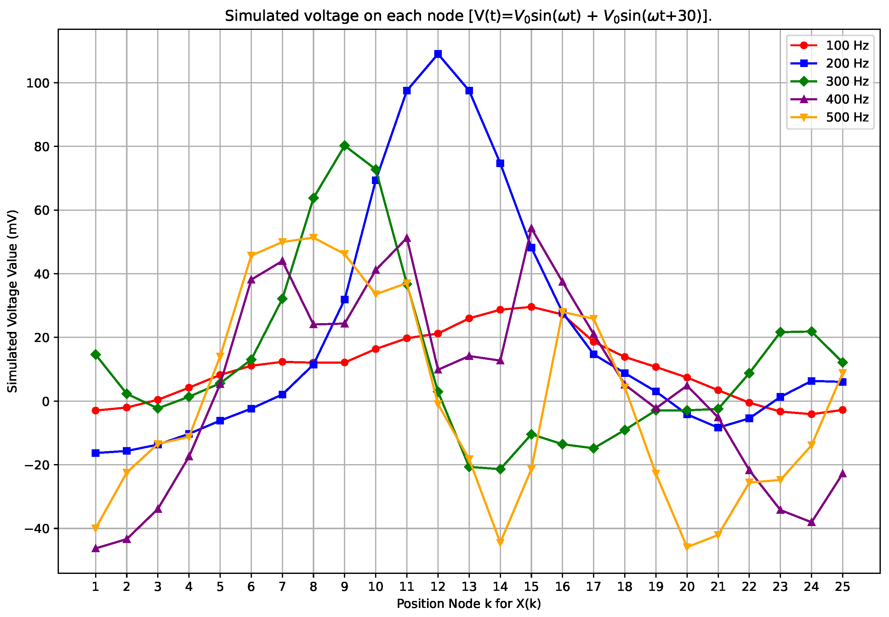
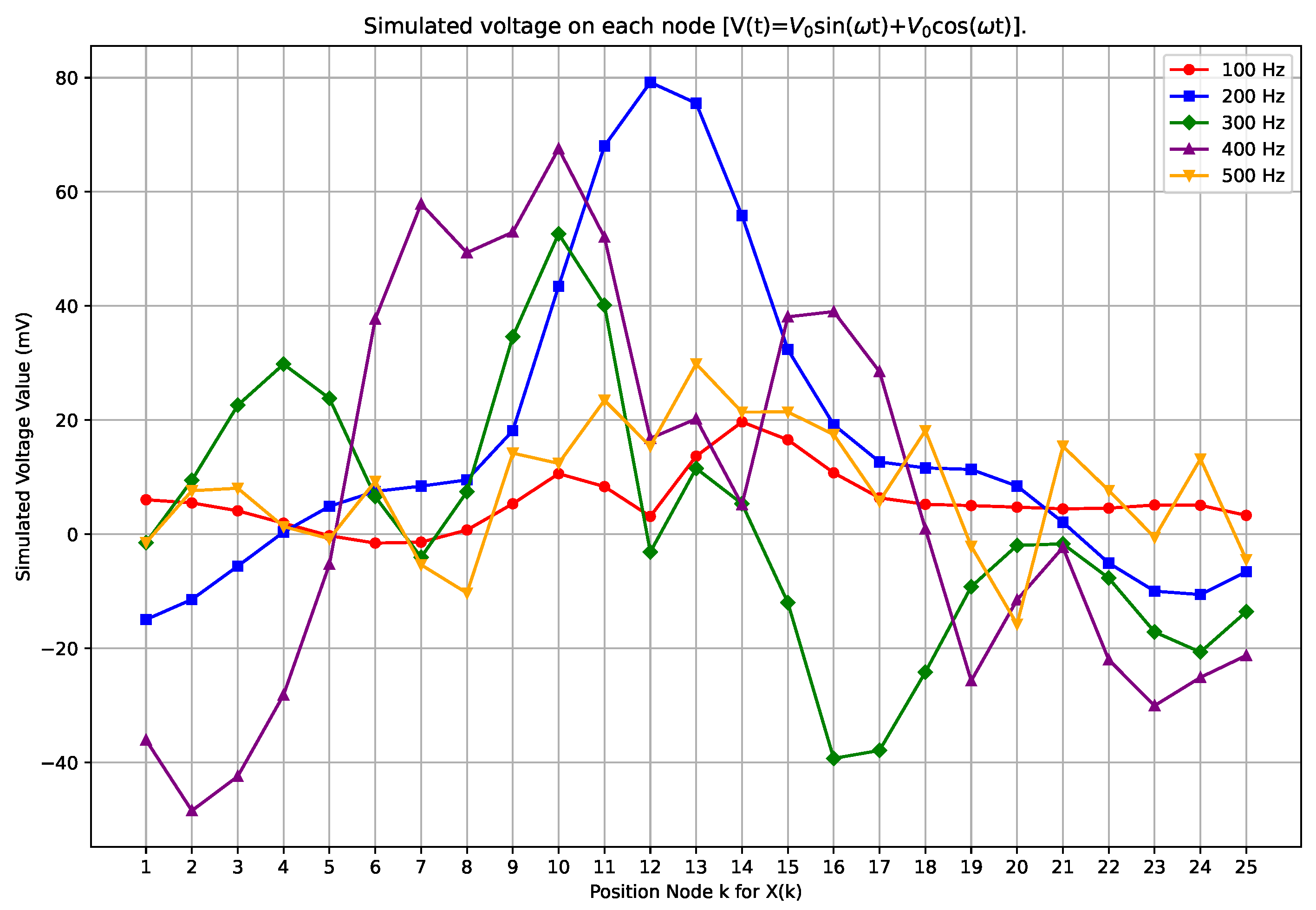
The data gathered from the simulation showed the voltage over time in each of the tested nodes, alongside the current in the node containing the signal generator. It is worth noting that proper Schroedinger equation solutions were obtained with the use of voltage generator for the case of two sinusoidal waves shifted by some phase (as from the circuit depicted in Figure 6) or by one sinusoidal wave (as from the circuit depicted in Figure 3) of given frequency as indicated by Figure 9 (with phase shift), Figure 10 (no phase shift), Figure 11 (with phase shift).
Based on the results of the simulations, the following conclusions can be made:
  • The circuit typically needs a few cycles to stabilize.
  • There is a visible spike in voltage at the point where the signal generator is located.
  • Achieving measurement at the point where the current flowing through the signal generator equals exactly zero was effectively impossible, due to the limits of the simulation software.
  • The circuit enables simulating any potential in spatial coordinates.
  • Various forms of wave functions characteristic for excited state was obtained as depicted in Figure 8, Figure 9, Figure 10 and Figure 11 while family of ground state wave-functions is depicted in Figure 4.
Based on the real experiments, the following conclusions can be made:
  • The circuit has a ground state solution that is equivalent to a ground state wave function as depicted in Figure 7 and Figure 12.
  • The first three excited states are well represented in Krons’s hardware model.
  • Higher energy states are more delocalized than lower energy states.

4. Derivation of Kron’s Model Expressed by a Long-Line Model and Its Generalization towards the Ginzburg–Landau Equation

A non-dissipative Schrödinger equation with real value potential and eigenenergy states can be expressed by Kron’s model with inductance in the horizontal direction, as well as by capacitance and non-uniform inductances in the vertical direction, as depicted in Figure 2 or Figure 13.
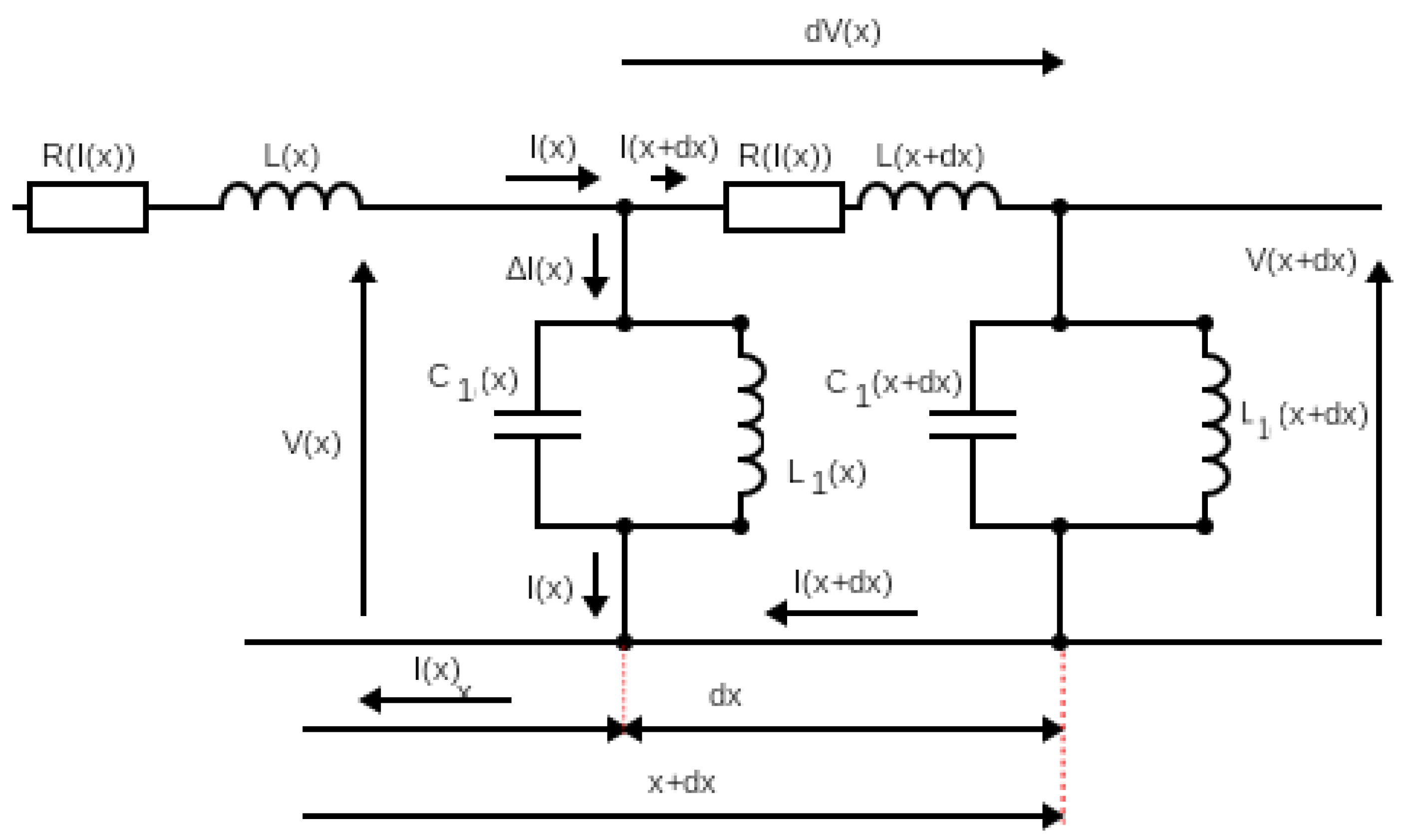
We can deform the transmission line by introducing non-linear resistive elements in series with inductances placed horizontally. Let us refer to the long-line model depicted in Figure 14, which can be characterized by the equations
d V ^ ( x ) = d x j L ω I ^ ( x ) , d I ^ ( x ) = d x ( 1 j L 1 ω + j ω C 1 ) V ^ ( x )
which imply
d d x V ^ ( x ) = j L ω I ^ ( x ) , d d x I ^ ( x ) = ( 1 j L 1 ω + j ω C 1 ) V ^ ( x ) ,
which results in the equation (when L = constant)
d 2 d x 2 V ^ ( x ) = j L ω ( 1 j L 1 ω + j ω C 1 ) V ^ ( x ) .
The last equation can be rewritten in the form
d 2 d x 2 V ^ ( x ) = ( L L 1 L C 1 ω 2 ) V ^ ( x ) = k 1 ( ω ) 2 V ^ ( x ) , k 1 ( ω ) = ( L L 1 L C 1 ω 2 )
and has the analytic solution
V ^ ( x ) = a 1 e + i k 1 x + a 2 e i k 1 x = = a 1 e + i ( L L 1 L C 1 ω 2 ) x + a 2 e i ( L L 1 L C 1 ω 2 ) x = b 1 s i n ( k 1 x ) + b 2 c o s ( k 1 x ) = = b 1 s i n ( ( L L 1 L C 1 ω 2 ) x ) + b 2 c o s ( ( L L 1 L C 1 ω 2 ) x ) , I ^ ( x ) = c 1 e + i k 1 x + c 2 e i k 1 x = = c 1 e + i ( L L 1 L C 1 ω 2 ) x + c 2 e i ( L L 1 L C 1 ω 2 ) x = = d 1 s i n ( + ( L L 1 L C 1 ω 2 ) x ) + d 2 c o s ( ( L L 1 L C 1 ω 2 ) x )
It is not hard to generalize the obtained result for the case of the R, L, and C circuit components in a series on the upper cable branch and for the case of circuit elements in parallel on the inter-connecting branch with values of R 1 , L 1 , and C 1 . We obtain the equations
d V ^ ( x ) = d x ( j L ω + R + 1 j ω C ) I ^ ( x ) , d I ^ ( x ) = d x ( 1 j L 1 ω + j ω C 1 + 1 R 1 ) V ^ ( x ) ,
which can be decoupled (if all capacitive, inductive, and resistive linear density elements are position-independent), so we have two independent equations:
d 2 d x 2 V ^ ( x ) = ( j L ω + R + 1 j ω C ) ( 1 j L 1 ω + j ω C 1 + 1 R 1 ) V ^ ( x ) = k 1 q 2 ( ω ) 2 V ^ ( x ) , d 2 d x 2 I ^ ( x ) = ( j L ω + R + 1 j ω C ) ( 1 j L 1 ω + j ω C 1 + 1 R 1 ) I ^ ( x ) = k 1 q ( ω ) 2 I ^ ( x ) .
In the next step, we can incorporate non-linear elements in the previously considered transmission line models. We obtain the situation depicted in Figure 14. First, we will consider a linear circuit with linear density (per unit length) of L ( x ) , L 1 ( x ) , and C 1 ( x ) . We obtain the equations
d V ^ ( x ) = d x j L ( x ) ω I ^ ( x ) , d I ^ ( x ) = d x ( 1 j L 1 ( x ) ω + j ω C 1 ( x ) ) V ^ ( x )
which imply
1 j L ( x ) ω d d x V ^ ( x ) = I ^ ( x ) , d d x ( 1 j L ( x ) ω d d x V ^ ( x ) ) = d d x I ^ ( x ) = ( 1 j L 1 ( x ) ω + j ω C 1 ( x ) ) V ^ ( x ) .
The last equation after differentiation implies the second-order equation with a dissipative term [ d d x ( 1 j L ( x ) ω ) ] :
( 1 j L ( x ) ω ) d 2 d x 2 V ^ ( x ) + ( d d x V ^ ( x ) ) [ d d x ( 1 j L ( x ) ω ) ] = ( 1 j L 1 ( x ) ω + j ω C 1 ( x ) ) V ^ ( x ) .
Hence, we obtain damped harmonic oscillator after multiplication by j ω
( 1 L ( x ) ) d 2 d x 2 V ^ ( x ) ( d d x V ^ ( x ) ) ( d d x L ( x ) ) + 1 L 1 ( x ) V ^ ( x ) = ( + ω 2 C 1 ( x ) ) V ^ ( x ) .
Under the assumption L ( x ) = c o n s t a n t s = L , we have
( 1 L ( x ) ) d 2 d x 2 V ^ ( x ) + 1 L 1 ( x ) V ^ ( x ) = ( + ω 2 C 1 ( x ) ) V ^ ( x ) ,
which is similar to the Schrödinger equation of the form
2 2 m d 2 d x 2 ψ ( x ) + V p ( x ) ψ ( x ) = E ψ ( x ) ,
indicating that energy E is related to + ω 2 C 1 ( x ) if we set capacitance independent of the position, so C 1 ( x ) = c o n s t 2 . Furthermore, with the assumption that V(x) is equivalent to the wave function ψ ( x ) , we can establish other analogies. We can notice that 1 L 1 ( x ) plays the role of the potential from the Schrödinger equation V p ( x ) , while 1 L ( x ) plays the role of 2 2 m .
Equation (18) can be subjected to renormalization of the electric circuit parameters by multiplication with 1 k constant, so the same shape of solutions V ( x ) is obtained.
( 1 k * L ( x ) ) d 2 d x 2 V ^ ( x ) + 1 k * L 1 ( x ) V ^ ( x ) = ( + ω k 2 C 1 ( x ) ) V ^ ( x )
Therefore, new renormalized circuit parameters (hardly scalable in a practical circuit design) are L r e n = k L , L 1 , r e n ( x ) = k L 1 ( x ) , and a new driving frequency was obtained ω r = ω k while keeping C 1 = C 1 , r e n unchanged, as described in Table 2.
The placement of linear resistance R in series with L inductance modifies the previous equation to
( 1 L + R j ω ) d 2 d x 2 V ^ ( x ) + 1 L 1 ( x ) V ^ ( x ) = ( + ω 2 C 1 ( x ) ) V ^ ( x ) ,
which gives
( j ω L j ω L + R ) 1 L d 2 d x 2 V ^ ( x ) + 1 L 1 ( x ) V ^ ( x ) = ( + ω 2 C 1 ( x ) ) V ^ ( x )
and, finally, implies
1 L d 2 d x 2 V ^ ( x ) + ( j ω L + R j ω L ) 1 L 1 ( x ) V ^ ( x ) = ( + ( j ω L + R j ω L ) ω 2 C 1 ( x ) ) V ^ ( x )
The introduction of resistor R brings renormalization of the effective potential V p , so it is complex-valued:
V p ( x ) = 1 L 1 ( x ) ( j ω L + R j ω L ) 1 L 1 ( x ) = ( 1 + R j ω ) 1 L 1 ( x ) = ( 1 j R ω ) 1 L 1 ( x )
and the renormalization of the energy eigenstates, which are also complex-valued as
ω 2 C 1 ω 2 C 1 ( 1 j R ω ) .
On the other hand, the placement of resistance R 1 in parallel with L 1 and C 1 gives the equation
( 1 L ) d 2 d x 2 V ^ ( x ) + 1 L 1 ( x ) + R 1 j ω V ^ ( x ) = ( + ω 2 C 1 ( x ) ) V ^ ( x ) ,
and thus, we have a dissipative effective Schrödinger potential associated with non-zero R 1 , given as
V p ( x ) = 1 L 1 ( x ) + R 1 j ω = j ω j ω L 1 ( x ) + R 1 = j ω ( j ω L 1 ( x ) + R 1 ) ( ω L 1 ( x ) ) 2 + R 1 2 = ( ω 2 L 1 ( x ) + j R 1 ω ) ( ω L 1 ( x ) ) 2 + R 1 2 .
Therefore, we obtain the imaginary part of the potential given as
I m [ V p ( x ) ] = j R 1 ω ( ω L 1 ( x ) ) 2 + R 1 2
and, still, the real values of the eigenenergy, which means that R 1 can represent some kind of vector potential. The most general version of the dissipative Schrödinger equation due to the presence of R and R 1 , which are position-independent, brings the equation
1 L + R j ω d 2 d x 2 V ^ ( x ) + 1 L 1 ( x ) + R 1 j ω V ^ ( x ) = ω 2 C 1 V ^ ( x )
that implies
j ω L j L ω + R 1 L d 2 d x 2 V ^ ( x ) + j ω j ω L 1 ( x ) + R 1 V ^ ( x ) = ω 2 C 1 V ^ ( x ) ,
so we have
1 L d 2 d x 2 V ^ ( x ) + 1 L j L ω + R j ω L 1 ( x ) + R 1 V ^ ( x ) = j L ω + R j ω L ω 2 C 1 V ^ ( x ) ,
so we arrive at the renormalization of the effective potential:
V p ( x ) = 1 L 1 ( x ) 1 L j L ω + R ( j ω L 1 ( x ) + R 1 ) ( j ω L 1 ( x ) + R 1 ) ( j ω L 1 ( x ) + R 1 ) = 1 L L L 1 ω 2 + R R 1 ( ( ω L 1 ( x ) ) 2 + R 1 2 ) + j 1 L ( R L 1 ( x ) ω + R 1 L ω ) ( ( ω L 1 ( x ) ) 2 + R 1 2 )
and the renormalization of the eigenvalues
E = ω 2 C 1 ω 2 C 1 ( 1 j R ω ) .

4.1. Case of Modeling a Quantum Roton by the Classical Electrical Transmission Line

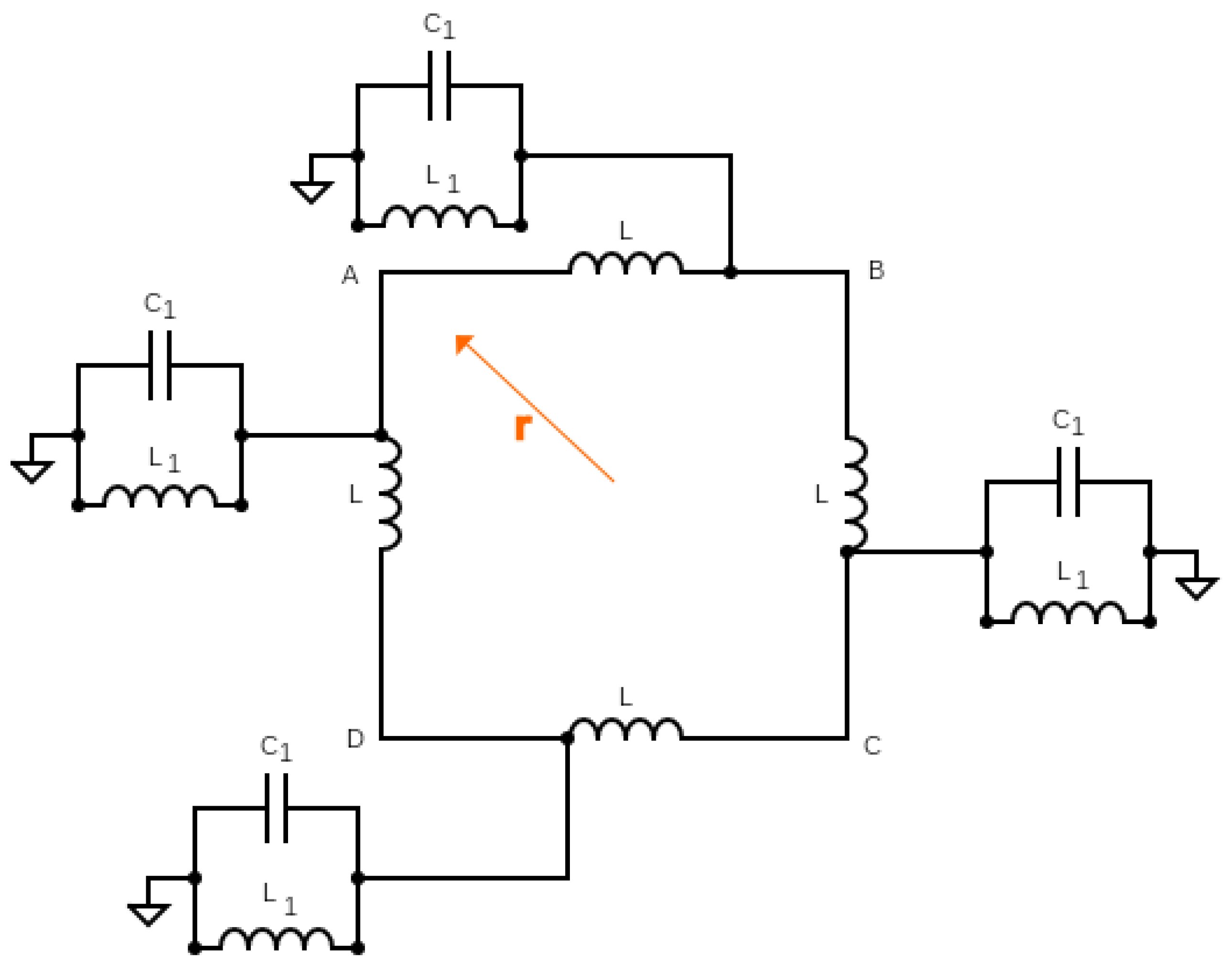
It is instructive to consider a particle trapped in a circular tunnel, so it moves around in a circle. Such a problem is known as a quantum roton, with radius r, as depicted in Figure 15. Under the assumption of voltage dependence on the position as analogical to quantum mechanics (the equivalence of the voltage phasor V ^ ( ϕ ) = V 0 ( ϕ ) e j ( ω t + γ ) = e j ( ω t + γ ) ψ ( ϕ ) = ψ ^ , where V 0 ( ϕ ) , γ , ω R ), we obtain
V ^ ( ϕ ) = V ^ s 1 a s i n ( r ϕ L ( + ω 2 C 1 1 L 1 ) ) + V ^ s 1 b c o s ( r ϕ L ( + ω 2 C 1 1 L 1 ) ) .
The following equation is fulfilled with a closed electrical line with rotational symmetry.
( 1 r 2 L ( ϕ ) ) d 2 d ϕ 2 V ^ k ( ϕ ) + 1 L 1 ( ϕ ) V ^ k ( ϕ ) = ( + ω k 2 C 1 ) V ^ k ( ϕ ) , E k = ( + ω k 2 C 1 ) , V ^ k ( ϕ ) = V ^ k ( ϕ + n 2 π )
At this stage, we have assigned frequency ω k to the phasor V ^ k ( ϕ ) . Clearly, E k plays the role of the k-th eigenenergy (eigenvalue). We observe that, due to the linearity of Equation (35), we obtain the form
( 1 r 2 L ( ϕ ) ) d 2 d ϕ 2 V ^ ( ϕ ) + 1 L 1 ( ϕ ) V ^ ( ϕ ) = k [ ( + a k ω k 2 C 1 ) V ^ k ( ϕ ) ] , V ^ ( ϕ ) = a k V ^ k ( ϕ + n 2 π ) ,
where a k is a complex or a real constant coefficient. Therefore, we can introduce the most generalized voltage or current phasor in the form
V ^ ( ϕ ) = ( k = 1 N a k V ^ k ( ϕ ) ) , I ^ ( ϕ ) = ( k = 1 N a k I ^ k ( ϕ ) )
The periodic boundary condition V ^ k ( ϕ ) = V ^ k ( ϕ + n 2 π ) implies V ^ ( ϕ ) = V ^ ( ϕ + n 2 π ) , and thus, we have
r 2 π L ( + ω 2 C 1 1 L 1 ) = 2 π n ( ) r ϕ L ( + ω 2 C 1 1 L 1 ) = ϕ n , V ^ ( ϕ ) = V ^ s 1 a s i n ( n 1 ϕ ) + V ^ s 1 b c o s ( n 1 ϕ ) = V ^ s 1 ( cos ( β 1 ) sin ( n 1 ϕ ) + sin ( β 1 ) cos ( n 1 ϕ ) ) = V ^ s 1 sin ( n 1 ϕ + β 1 ) = | V ^ s 1 a | 2 + | V ^ s 2 b | 2 ( cos ( A r c T a n [ V ^ s 1 b V ^ s 1 a ] ) sin ( n 1 ϕ ) + sin ( A r c T a n [ V ^ s 1 b V ^ s 1 a ] ) cos ( n 1 ϕ ) ) = | V ^ s 1 a | 2 + | V ^ s 2 b | 2 sin ( n 1 ϕ + A r c T a n [ V ^ s 1 b V ^ s 1 a ] ) , V ^ s 1 a = V ^ s 1 cos ( β 1 ) , V ^ s 1 b = V ^ s 1 sin ( β 1 ) , V ^ s 1 b V ^ s 1 a = t a n ( β 1 ) , β 1 = A r c T a n [ V ^ s 1 b V ^ s 1 a ] , | V s 1 | = | V ^ s 1 a | 2 + | V ^ s 2 b | 2 .
Hence, for the n-th eigenvalue level, we have
1 L C 1 n 2 R 2 + 1 C 1 L 1 = ω n 2 .
The ground energy (eigenvalue) of the system, thus, corresponds to M i n ( ω ) = ω g = 1 C 1 L 1 , and clearly, the energy levels (eigenvalues) are quantized. We observe that the phasors of the structure:
V ^ ( ϕ ) = V ^ s 1 a s i n ( n 1 ϕ ) + V ^ s 1 b c o s ( n 1 ϕ ) + V ^ s 2 a s i n ( n 2 ϕ ) + V ^ s 2 b c o s ( n 2 ϕ ) + = V ^ s 1 a s i n ( 1 r ϕ L ( + ω 2 C 1 1 L 1 ) ) + V ^ s 1 b c o s ( 1 r ϕ L ( + ω 2 C 1 1 L 1 ) ) + V ^ s 2 a s i n ( 2 r ϕ L ( + ω 2 C 1 1 L 1 ) ) + V ^ s 2 b c o s ( 2 r ϕ L ( + ω 2 C 1 1 L 1 ) ) + = k = + ( V ^ s k a s i n ( k ϕ ) + V ^ s k b c o s ( k ϕ ) ) = V ^ ( ϕ ) = V ^ ( ϕ + s 2 π ) .
are also the solution of the equation given by Equation (36). We recognize that, in the case of a roton, we have different integer values of s and k and the following orthogonality relation holds: 0 2 Π d ϕ V ^ k ( ϕ ) V ^ s ( ϕ ) = δ s , k . Therefore, in a very real way, the phasors V ^ s ( k ) ( ϕ ) play the role of the k-th eigenfunction (quasi-wave function) in the roton model, since sin ( k ϕ ) and sin ( s ϕ ) are orthogonal. Contrary to quantum mechanics, V ^ s ( k ) ( ϕ ) does not need to be normalized to 1, but we can still assume a priori that it is possible, as it depends on a proper setup of the physical system. Using the aforementioned orthogonality and Equation (36) (and by setting the k-th mode occupancy coefficient | a k | 2 giving the QM probability of the k-th energy level | a k | = | V ^ s k a | 2 + | V ^ s k b | 2 ), we obtain the relation
( k = + | a k | 2 k 2 ) r 2 L + k = + | a k | 1 L 1 = k = + | a k | 2 C 1 ω k 2 = E e f f = E .
Once we have a given sequence of V ^ s k a and V ^ s k b , we can establish the value for effective energy E e f f . However, a certain difference is that E e f f can be arbitrarily high, as k = + | a k | 2 does not need to be normalized to one, but again, it can be. Spectrum decomposition of E is quite the same as in the case of the total energy of a quantum particle described by the Schrödinger equation. We determine the k-th current phasor as
I ^ k ( ϕ ) = 1 j ω k L 1 r d d ϕ V ^ k ( ϕ ) = L ( + ω k 2 C 1 1 L 1 ) j ω k L V ^ s 1 a c o s ( r ϕ L ( + ω k 2 C 1 1 L 1 ) ) V ^ s 1 b s i n ( r ϕ L ( + ω k 2 C 1 1 L 1 ) ) = k r j ω k L V ^ s 1 a c o s ( k ϕ ) V ^ s 1 b s i n ( k ϕ ) = k r j ω k L c o s ( β + k ϕ ) = L ( + ω k 2 C 1 1 L 1 ) j ω k L [ V ^ s 1 a c o s ( β ) c o s ( β ) c o s ( r ϕ L ( + ω k 2 C 1 1 L 1 ) ) V ^ s 1 b s i n ( β ) s i n ( r ϕ L ( + ω k 2 C 1 1 L 1 ) ) ] = L ( + ω k 2 C 1 1 L 1 ) j ω k L V ^ s 1 c o s ( β + r ϕ L ( + ω k 2 C 1 1 L 1 ) ) , V ^ s 1 a c o s ( β ) = V ^ s 1 , V ^ s 1 a s i n ( β ) = V ^ s 1 , A r c T a n [ V ^ s 1 a V ^ s 1 b ] = β
and in the generalized version:
I ^ ( ϕ ) = k = k = + a k I ^ ( ϕ , ω k ) = k = k = + 1 j ω k L a k 1 r d d ϕ V ^ ( ϕ , ω k ) = k = k = + j L ( + ω k 2 C 1 1 L 1 ) ω k L [ V ^ s k ( t 0 ) e j ( ω k t + γ k ) cos ( β k + r ϕ L ( + ω k 2 C 1 1 L 1 ) ) ] = k = k = + j k r ω k L [ V ^ s k ( t 0 ) e j ( ω k t + γ k ) cos ( β k + k ϕ ) ] , R e [ I ^ ( ϕ , t ) ] = k = k = + L ( + ω k 2 C 1 1 L 1 ) ω k L [ V s k ( t 0 ) × c o s [ ( ω k ( t t 0 ) + γ k π 2 ) ] cos ( β k + r ϕ L ( + ω k 2 C 1 1 L 1 ) ) ] = k = k = + k r ( 1 L C 1 k 2 r 2 + 1 C 1 L 1 ) L [ V s k ( t 0 ) c o s [ ( ( 1 L C 1 k 2 r 2 + 1 C 1 L 1 ) ( t t 0 ) + γ k π 2 ) ] cos ( β k + k ϕ ) ] , R e [ V ^ ( ϕ , t ) ] = k = k = + [ V s k ( t 0 ) c o s [ ( ω k ( t t 0 ) + γ k ) ] sin ( β k + r ϕ L ( + ω k 2 C 1 1 L 1 ) ) ] , k = k = + [ V s k ( t 0 ) c o s [ ( ( k 2 r 2 1 L C 1 + 1 L C ) ( t t 0 ) + γ k ) ] sin ( β k + k ϕ ) ] ,
where R e [ I ^ ( ϕ , t ) ] and R e [ V ^ ( ϕ , t ) ] stand for the physically observable electric current and voltage, while t 0 , V s k ( t 0 ) = a k , and γ k stand for different real-valued numbers being open parameters, depending on the initial boundary conditions with k of the integer value ranging from minus to plus infinity.

4.2. Case of Non-Linear Transmission Line Model Generalization of Kron’s Model

We consider a transmission line with inductance depending vertically on space, given by L 1 ( x ) , while assuming a priori other passive elements to be constant. We obtain
d d x I ^ ( x ) = ( j ω C 1 + 1 j ω L 1 ( x ) ) V ^ ( x ) , d d x V ^ ( x ) = ( j ω L + R ( I ( x ) ) ) I ^ ( x ) ,
and we obtain
d d x I ^ ( x ) = d d x ( 1 ( j ω L + I ( x ) R ( I ( x ) ) ) d d x V ^ ( x ) ) = ( j ω C 1 + 1 j ω L 1 ( x ) ) V ^ ( x ) .
In the general case, we drop the assumption a priori that I and V are phasors, and we have
d d x I ( x , t ) = ( d d t V ( x , t ) C 1 t 0 t d t 1 L 1 ( x ) V ( x , t ) ) , d d x V ( x ) = ( L d I d t + I ( x ) R ( I ( x ) ) ) .
In the case of introducing non-linear resistance in series with upper inductors and under the assumption of the uniformity of the transmission line with explicitly given dependence on the linear inductance density L 1 ( x ) , we arrive at a non-linear integro-differential equation. Consequently, we obtain
d 2 d x 2 I ( x , t ) = ( d d t d d x V ( x , t ) C 1 t 0 t d t d d x [ 1 L 1 ( x ) V ( x , t ) ] ) , d d x V ( x ) = ( L d I d t + I ( x ) R ( I ( x ) ) ) ,
which results in
d 2 d x 2 I ( x , t ) = ( d d t C 1 ( L d I d t + I ( x ) R ( I ( x ) ) ) + t 0 t d t [ d d x 1 L 1 ( x ) ] V ( x , t ) + t 0 t d t 1 L 1 ( x ) [ d d x V ( x , t ) ] ) , d d x V ( x ) = ( L d I d t + I ( x ) R ( I ( x ) ) ) ,
and applying the operator d dt results in
d 3 d x 2 d t I ( x , t ) = d d t ( d d t C 1 ( L d I d t + I ( x ) R ( I ( x ) ) ) + [ d d x 1 L 1 ( x ) ] V ( x , t ) ) + 1 L 1 ( x ) [ d d x V ( x , t ) ] , d d x V ( x ) = ( L d I d t + I ( x ) R ( I ( x ) ) ) ,
which brings
d d x [ 1 [ d d x 1 L 1 ( x ) ] [ d 3 d x 2 d t I ( x , t ) d d t ( d d t C 1 ( L d I d t + I ( x ) R ( I ( x ) ) ) + 1 L 1 ( x ) [ L d I d t + I ( x ) R ( I ( x ) ) ] ] ] = ( L d I d t + I ( x ) R ( I ( x ) ) ) = d d x V ( x ) .
Consequently, we end up with a non-linear partial differential equation for I ( x , t ) in the form
d d x ( 1 [ d d x 1 L 1 ( x ) ] ) ] [ d 3 d x 2 d t I ( x , t ) + d d t ( d d t C 1 ( L d I ( x , t ) d t + I ( x , t ) R ( I ( x , t ) ) ) + 1 L 1 ( x ) [ L d I ( x , t ) d t + I ( x , t ) R ( I ( x , t ) ) ] ] + [ [ ( 1 [ d d x 1 L 1 ( x ) ] ) ] d d x [ d 3 d x 2 d t I ( x , t ) + d d t ( d d t C 1 ( L d I ( x , t ) d t + I ( x , t ) R ( I ( x , t ) ) ) + 1 L 1 ( x ) [ L d I d t + I ( x , t ) R ( I ( x , t ) ) ] ] ] = ( L d I ( x , t ) d t + I ( x ) R ( I ( x , t ) ) ) = d d x V ( x ) ,
where L, R, and C 1 are considered to be non-dependent on x and they represent the upper inductance, linear or non-linear resistance, and capacitance C 1 , while L 1 ( x ) is the inductance linear density, which is explicitly position-dependent.
In the first approach, it is instructive to consider non-linear resistance as represented by two identical diodes connected in an anti-parallel way in the forward conductive direction. In such a case, the non-linear static resistance is given by the formula
R ( I ) = V I = k T l n ( I I 0 ) + 1 I = V I 0 ( e V k T 1 ) = R ( V ) .
Under the circumstance of low voltage, R ( V 0 ) = k T I 0 , while for non-small values of voltage, we can assume R ( V ) = V I 0 e ( V k T ) .

5. Linearized Ginzburg–Landau Equation Represented by RLC Transmission Line

We start from the circuit depicted in Figure 16, which is a modification of the original Kron electric line from Figure 2. We replace the inductance linear density in the horizontal direction with capacitance linear density C ( x ) .
Then,
d V ^ = d x ( 1 j ω C ( x ) ) I ^ ( x ) , d I ^ = d x ( 1 j ω L 1 ( x ) + j ω C 1 ( x ) ) V ^ ( x ) ,
and thus, we have
d d x V ^ = ( 1 j ω C ( x ) ) I ^ ( x ) , d 2 d x 2 I ^ = ( 1 j ω L 1 ( x ) + j ω C 1 ( x ) ) d d x V ^ ( x ) V ^ ( x ) ( d d x 1 j ω L 1 ( x ) + j ω d d x C 1 ( x ) ) .
Finally, this can be written as an integro-differential equation of the form
d 2 d x 2 I ( x , t ) = ( 1 j ω L 1 ( x ) + j ω C 1 ( x ) ) ( 1 j ω C ( x ) ) I ( x ) + + [ x 0 x d x 1 ( 1 j ω C ( x 1 ) ) I ^ ( x 1 ) ] ( d d x 1 j ω L 1 ( x ) + j ω d d x C 1 ( x ) )
If we assume L 1 ( x ) = c o n s t 1 and C 1 ( x ) = c o n s t 2 , our integro-differential equation becomes a differential equation d 2 d x 2 I = ( 1 ω L 1 + ω C 1 ) ( 1 ω C ( x ) ) I ( x ) , and consequently, we obtain the equation for the structure of a one-dimensional time-independent Ginzburg–Landau equation with no magnetic field (no vector potential), with the equivalence of the phasor I ^ to the macroscopic GL wave function ψ , so
L 1 d 2 d x 2 I ^ ( x ) = ( 1 ω L 1 C 1 ) ( 1 ω C ( x ) ) I ^ ( x ) , I ^ ( x ) = ψ ( x ) , 2 2 m d 2 d x 2 ψ ( x ) = α ( x ) ψ ( x ) , α ( x ) = ( 1 ω + L 1 C 1 C ( x ) ) 1 ω , L 1 = 2 2 m ,
where α ( x ) stands for the standard coefficient of GL theory, expressing the strength of superconductivity, and where we have dropped the β coefficient expressing the non-linear term β ( x ) | ψ ( x ) | 2 ψ ( x ) . By space modulation of C 1 ( x ) , we can obtain superconducting and non-superconducting regions of the superconductor, as represented by a transmission electrical line.
Approaching full representation of the Ginzburg–Landau equation by the RLC circuit can be obtained by the usage of varactors and tunneling diodes controlled by constant biasing voltage, as mentioned by Pluszyński [22].
It is worth noticing that the Schrödinger equation can also be represented by the circuit diagram from Figure 16. From there and Equations (53), we obtain
d 2 d x 2 V = ( 1 j ω C ( x ) ) d d x I ( x ) + I ( x ) d d x ( 1 j ω C ( x ) )
Thus, under the assumption C ( x ) = c o n s t , we arrive at the equation
d 2 d x 2 V = ( 1 j ω C ) d d x I ( x ) = ( 1 j ω C ) ( 1 j ω L 1 ( x ) + j ω C 1 ( x ) ) V ( x ) ,
which, with L 1 = const , the precondition can be simplified into the form:
L 1 d 2 d x 2 V = ( + 1 C ω 2 L 1 C 1 ( x ) C ) V ( x ) .
It is, thus, interesting to obtain the Schrödinger equation, where 2 2 m = L 1 and with the eigenenergy given by E = + 1 C ω 2 , while V e f f ( x ) = L 1 C 1 ( x ) C .

6. Conclusions

The conducted numerical simulations show the possibility of generalizing the circuits originally proposed by Kron to represent a confined particle by different shapes of effective potential, namely the harmonic, V-shaped, or polynomially dependent case. A quantum roton model was implemented in a classical electrical transmission line LC closed circuit. The case of a circuit implementing a linearized Ginzburg–Landau equation was identified and analyzed, as depicted in Figure 16. Two different types of circuits representing the Schrödinger linear equation were determined, as given in Figure 2 and Figure 16. The case of two electrostatically coupled rotons with Coulomb repulsion (or attraction in the case of a hole and electron), mimicking two separated single electrons, each in a different single-electron semiconductor ring, has not yet been tackled and represented by RLC analog electronic circuits, as initially indicated by Pluszyński [22].
The miniaturization of the specified RLC circuit models is quite straightforward and opens the perspective of the massive implementation of an analog electronics solver for Schrödinger equations based on Kron’s second circuit. Such hardware could potentially vastly improve the speed and efficiency of simulations of quantum phenomena, such as single photons hitting superconducting detectors, as one can conduct hardware simulation with the omission of various software layers. The presented concepts could result in the development of small classical chips simulating quantum phenomena locally. Various simulation methodologies presented in [24,25,26] shall be applied in more advanced versions of the analog solver of the Schrödinger equation.
Other future work should be focused on the representation of superconducting single-photon detectors [27] and Josephson junctions [28,29] by classical analog electronics, as already discussed. Furthermore, various moving topological defects in the parameter order as described by Stepien and Pomorski [25,30] should be within the technological scope of RLC circuits with varactors biased by DC and AC voltages. A particularly interesting feature is the representation of the Josephson transmission line expressed as a two-fluid model by mixed analog–digital electronic circuits with methodology specified by [24]. Another class of physical phenomena as given by [26,31] can be also expressed by generalized Kron’s methodology and is the subject of future implementations in the form of integrated circuits.

Author Contributions

Conceptualization, K.P.; Methodology, K.P.; Validation, Ł.P. and E.H.; Formal analysis, K.P.; Writing—review & editing, K.P. and Ł.P.; Visualization, Ł.P. and E.H. All authors have read and agreed to the published version of the manuscript.

Funding

Quantum Hardware Systems and Lodz University of technology provided materials and equipment for conducted research.

Data Availability Statement

The original contributions presented in the study are included in the article, further inquiries can be directed to the corresponding author.

Acknowledgments

This work was conducted with contributions of 45% by the first author, 40% by the second author, and 15% by the third author. The conceptual and mathematical framework was developed by the first author, while the second author implemented and carried out all simulations [22]. Voltage measurements on the constructed circuit were performed by the third author, who is an active member of the Schrödinger Cat scientific club (Kot Schroedingera) at Lodz University of Technology, Institute of Physics, and also represents the company Quantum Hardware Systems. Language corrections were made by Inez Łuczywek and John Speller from Lodz University of Technology.

Conflicts of Interest

The authors declare no conflicts of interest.

References

  1. Kankanamge, G.; Udayanga, N. Continuous-Time Algorithms and Analog Integrated Circuits for Solving Partial Differential Equations. Ph.D. Thesis, Florida International University, Miami, FL, USA, 2019. [Google Scholar]
  2. Dirac, P.A.M. Principles of Quantum Mechanics; Oxford University Press: Oxford, UK, 1958. [Google Scholar]
  3. Fitzpatrick, R. Quantum Mechanics; World Scientific Publishing: Singapore, 2015. [Google Scholar]
  4. Binney, J.; Skinner, D. The Physics of Quantum Mechanics; Oxford University Press: Oxford, UK, 2013. [Google Scholar]
  5. Motta, M.; Rice, J.E. Emerging quantum computing algorithms for quantum chemistry. WIREs Comput. Mol. Sci. 2022, 12, e1580. [Google Scholar] [CrossRef]
  6. Streif, M.; Neukart, F.; Leib, M. Solving Quantum Chemistry Problems with a D-Wave Quantum Annealer. In Quantum Technology and Optimization Problems, QTOP; Lecture Notes in Computer Science; Springer: Berlin/Heidelberg, Germany, 2019; Volume 11413. [Google Scholar]
  7. Kron, G. Electric Circuit Models of the Schrödinger Equation; General Electric Company: Boston, MA, USA, 1944. [Google Scholar]
  8. Kouzaev, G.A. Circuit Approach for Simulation of EM-quantum Components. Applications of Advanced Electromagnetics. In Applications of Advanced Electromagnetics; Lecture Notes in Electrical Engineering; Springer: Berlin/Heidelberg, Germany, 2013; Volume 169. [Google Scholar]
  9. Kouzaev, G.A. Calculation of linear and nonlinear Schrödinger equations by the equivalent network approach and envelope technique. Mod. Phys. Lett. B 2010, 24, 1. [Google Scholar] [CrossRef]
  10. Edwards, M. Designing a Hybrid Digital/Analog Quantum Physics Emulator as Open Hardware. arXiv 2023, arXiv:2302.00821. [Google Scholar]
  11. Mourya, S.; Cour, B.R.L.; Sahoo, B.D. Emulation of Quantum Algorithms Using CMOS Analog Circuits. IEEE Trans. Quantum Eng. 2023, 4, 3102116. [Google Scholar] [CrossRef]
  12. Caruso, M. How classical circuits can simulate quantum aspects. arXiv 2022, arXiv:2209.10402. [Google Scholar]
  13. Blackwell, J.; Fewer, D.; Allen, L.; Cass, R. An Audio-Frequency Circuit Model of the One-Dimentional Schroedinger Equation and Its Sources of Error. Can. J. Phys. 2011, 33, 483–491. [Google Scholar] [CrossRef]
  14. Borgarino, M. Circuit-Based Compact Model of Electron Spin Qubit. Electronics 2022, 11, 526. [Google Scholar] [CrossRef]
  15. Rieger, C. Classical Simulability of Quantum Circuits; TU Munich, CERN: Munich, Germany, 2023. [Google Scholar]
  16. Nagai, N.; Takashi, Y. Circuit Theory Based on New Concepts and Its Application to Quantum Theory 8: Application of Circuit Theory to Schrödinger Equation. J. Signal Process. 2017, 21, 37–45. [Google Scholar] [CrossRef]
  17. Kengne, E.; Liu, W.; English, Q.L.Q.; Malomed, B.A. Ginzburg–Landau models of nonlinear electric transmission networks. Phys. Rep. 2022, 982, 1–124. [Google Scholar] [CrossRef]
  18. Lee, C.H.; Imhof, S.; Berger, C.; Bayer, F.; Brehm, J.; Molenkamp, L.W.; Kiessling, T.; Thomale, R. Topolectrical Circuits. Commun. Phys. 2018, 1, 39. [Google Scholar] [CrossRef]
  19. Pomorski, K.; Stojewski, B. Hybrid Schrödinger-Ginzburg–Landau (Sch-GL) approach to study of superconducting integrated structures. Mol. Cryst. Liq. Cryst. 2024, 768, 101–116. [Google Scholar] [CrossRef]
  20. Analog Devices: Analog Electronics Tutorials. Available online: https://www.analog.com/en/resources/simulation-models/spice-models.html (accessed on 1 January 2020).
  21. LTspice Community Documentation Supplement. Available online: https://ltwiki.org (accessed on 1 January 2020).
  22. Pluszyński, Ł. Analog Electric Computational Architectures and Simulation Techniques Modeling Quantum Processes and Quantum Devices. Master’s Thesis, Cracow Univesity of Technology, Kraków, Poland, 2023. [Google Scholar]
  23. Circuit Diagram: Circuit Diagram Free Circuit Design Application. Available online: https://www.circuit-diagram.org/ (accessed on 1 January 2020).
  24. Zubert, M.; Jankowski, M.; Kulesza, Z.; Napieralski, A. Modelling of Transmission Lines Inside Modern Integrated Semiconductor and Test Boards. IEEE Access 2021, 9, 87182–87195. [Google Scholar] [CrossRef]
  25. Stepien, L.; Pomorski, K. Bogomolny approach in description of superconducting structures. arXiv 2023, arXiv:2308.09172. [Google Scholar]
  26. Ezawa, M. Electric-circuit simulation of the Schrödinger equation and non-Hermitian quantum walks. Phys. Rev. B 2019, 100, 165419. [Google Scholar] [CrossRef]
  27. Irwin, D.; Hilton, G.C. Transition-edge sensors. In Cryogenic Particle Detection; Enss, C., Ed.; Springer: Berlin/Heidelberg, Germany, 2005. [Google Scholar]
  28. Pomorski, K.; Bednorz, A. Justification of the canonical quantization of the Josephson effect and its modifications due to high capacitance energy. J. Phys. A Math. Theor. 2016, 49, 125002. [Google Scholar] [CrossRef]
  29. Pomorski, K.; Giounanlis, P.; Blokhina, E.; Leipold, D.; Pęczkowski, P.; Staszewski, R.B. From two types of electrostatic position-dependent semiconductor qubits to quantum universal gates and hybrid semiconductor-superconducting quantum computer. In Superconductivity and Particle Accelerators; SPIE: Bellingham, WA, USA, 2019; Volume 11054. [Google Scholar]
  30. Stepien, L. Bogomolny equation for the BPS Skyrme model from strong necessary conditions. J. Phys. A Math. Theor. 2016, 49, 175202. [Google Scholar] [CrossRef]
  31. Malz, D.; Cirac, J. Few-Body Analog Quantum Simulation with Rydberg-Dressed Atoms in Optical Lattices. PRX Quantum 2023, 4, 020301. [Google Scholar] [CrossRef]
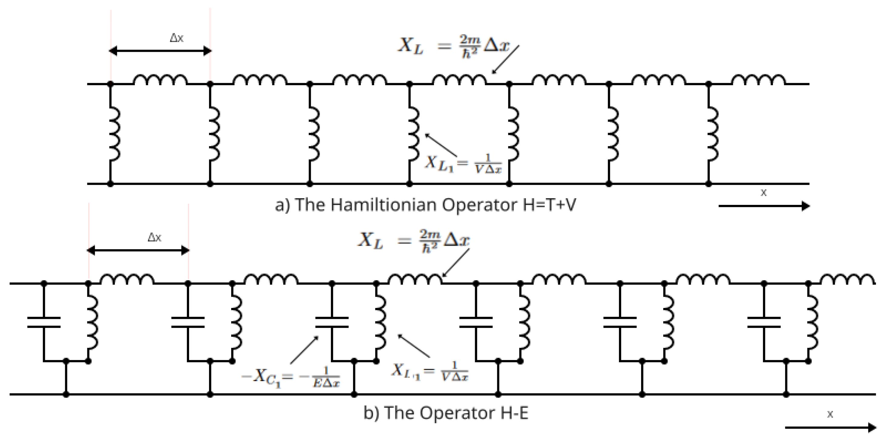
Figure 1. Hamiltonian operator (a) and H E operator (b) as described by Kron [7].
Condensedmatter 09 00035 g001
Figure 2. Conceptual schematic of circuit simulating a particle in a potential well in one dimension with voltage across the lower and upper branches as wave function values, as described by Kron [7].
Condensedmatter 09 00035 g002
Figure 5. Case of experimentally tested LC circuit with 19 nodes simulating particle in rectangular potential, where all capacitances C i = 1 μ F and all inductances L j = 1.5 mH .
Condensedmatter 09 00035 g005
Figure 6. Scheme of a classical RLC circuit with 25 nodes for the simulation of a quantum particle in a rectangular potential well with complex driving signals with V ( t ) = s i n ( ω t ) + s i n ( ω t + 30 ) .
Condensedmatter 09 00035 g006
Figure 9. Simulation results for a signal of two added sine waves, where the second one is shifted in phase by a factor of 30.
Condensedmatter 09 00035 g009
Figure 10. Simulation results for a signal of a sine wave with double the relative amplitude V 0 .
Condensedmatter 09 00035 g010
Figure 11. Simulation results for a signal obtained from adding sine and cosine waves with the same relative amplitude V 0 . All the simulations were run with the gear integration method, and an alternate solver was set as the simulation parameters in the LTspice freeware with the values specified in Table 2. Results obtained for low frequencies are depicted in Figure 12.
Condensedmatter 09 00035 g011
Figure 12. Case of experiment results for a rectangular potential LC line subjected to a signal frequency generator corresponding to the 1st and the 2nd excited state, in accordance with Figure 5.
Condensedmatter 09 00035 g012
Figure 13. Kron’s model in relation to a non-dissipative non-uniform transmission line model based on passive linear elements that are space-dependent: inductance and capacitance.
Condensedmatter 09 00035 g013
Figure 14. Kron’s model in relation to a transmission line model that is subjected to non-linear deformation introduced by non-linear resistive elements.
Condensedmatter 09 00035 g014
Figure 15. Circular LC transmission line mimicking a qubit roton.
Condensedmatter 09 00035 g015
Figure 16. LC circuit model representing the linearized Ginzburg–Landau equation.
Condensedmatter 09 00035 g016
Disclaimer/Publisher’s Note: The statements, opinions and data contained in all publications are solely those of the individual author(s) and contributor(s) and not of MDPI and/or the editor(s). MDPI and/or the editor(s) disclaim responsibility for any injury to people or property resulting from any ideas, methods, instructions or products referred to in the content.