Article

A Configurable 64-Channel ASIC for Cherenkov Radiation Detection from Space

by
Andrea Di Salvo
1,*,
Sara Garbolino
1,
Marco Mignone
1,
Stefan Cristi Zugravel
1,2,
Angelo Rivetti
1,
Mario Edoardo Bertaina
1,3 and
Pietro Antonio Palmieri
1,3
1
Section of Torino, Istituto Nazionale di Fisica Nucleare, INFN, 10125 Turin, Italy
2
Department of Electronics and Telecommunications, Politecnico di Torino, 10129 Turin, Italy
3
Physics Department, University of Torino (UniTO), 10124 Turin, Italy
*
Author to whom correspondence should be addressed.
Instruments 2023, 7(4), 50; https://doi.org/10.3390/instruments7040050
Submission received: 20 October 2023 / Revised: 21 November 2023 / Accepted: 26 November 2023 / Published: 7 December 2023

Abstract

:
This work presents the development of a 64-channel application-specific integrated circuit (ASIC), implemented to detect the optical Cherenkov light from sub-orbital and orbital altitudes. These kinds of signals are generated by ultra-high energy cosmic rays (UHECRs) and cosmic neutrinos (CNs). The purpose of this front-end electronics is to provide a readout unit for a matrix of silicon photo-multipliers (SiPMs) to identify extensive air showers (EASs). Each event can be stored into a configurable array of 256 cells where the on-board digitization can take place with a programmable 12-bits Wilkinson analog-to-digital converter (ADC). The sampling, the conversion process, and the main digital logic of the ASIC run at 200 MHz, while the readout is managed by dedicated serializers operating at 400 MHz in double data rate (DDR). The chip is designed in a commercial 65 nm CMOS technology, ensuring a high configurability by selecting the partition of the channels, the resolution in the interval 8–12 bits, and the source of its trigger. The production and testing of the ASIC is planned for the forthcoming months.

1. Introduction

Ultra-high energy cosmic rays (UHECRs) and neutrinos (UHENUs) passing through the atmosphere generate extensive air showers (EASs). The relativistic particles produced in the cascade emit Cherenkov light collimated with the direction of the EAS propagation which can be used to track the direction and the energy of the parent UHECR/UHENU. A telescope based on an optical system that focuses the light on a focal plane made of SiPMs can image such light and derive the EAS parameters. The signal induced in the sensor from sub-orbital height such as ∼30–40 km or low Earth orbit (LEO), such as a ∼500 km height, has a time extension of tens of nanoseconds. This result shows a dependance from the angle between the EAS direction and the axis marked out by the telescope according to simulations. This very short time extension of the signal demands a sampling rate of at least 100 MHz to achieve the required time resolution. In addition, the store of a waveform associated to the event allows for the discrimination of the EAS-related event from those originated by direct cosmic ray hits. Due to these requirements, the implementation of an ASIC is mandatory and its design is inspired by present and future projects in the field of UHECR and UHE neutrino astronomy such as Extreme Universe Space Observatory-Super Pressure Balloon 2 (EUSO-SPB2) [1], an on-board stratospheric balloon platform, or Terzina [2] and POEMMA [3] space-based missions.
The EUSO-SPB2 mission used a NASA Super Pressure Balloon for a test flight and it flew on 13 May 2023 from Wanaka (New Zealand). Unfortunately, the balloon developed a hole in the envelope and was terminated over the Pacific Ocean after only about 37 h of flight. The payload is composed of two telescopes, one devoted to fluorescence light measurements from UHECR EAS with energy above 1 EeV by pointing a multi-anode photo-multiplier tube (MAPMT) camera to nadir. The other telescope is reserved for the Cherenkov emission of CR EAS, with an energy target above 1 PeV, by collecting the Cherenkov light with a focal surface made of SiPMs. The latter instrument is based on a modified Schmidt telescope of 1m diameter, where four mirrors focus the light in two points on the camera area. This bifocal alignment is adopted to reduce the background noise discriminating the light that comes from outside the telescope tube (namely, two spots) and a direct cosmic ray (one spot). The SiPMs are provided by Hamamatsu and the pixel camera is formed by 512 units. The integration time is 10 ns and the system can readout 512 frames centered around the trigger point with a field-of-view (FoV) of 6.4° in zenith and 12.8° in azimuth. The entire telescope can be rotated from a horizontal level to 10° below the terrestrial limb. The JEM-EUSO collaboration is currently planning a new NASA SPB mission named POEMMA-Balloon with Radio (PBR) with a targeted launch in 2026. The payload will be a single telescope hosting both a fluorescence and a Cherenkov camera as conceived for the POEMMA mission.
NUSES [4] is an orbital mission whose target is the study of the Sun–Earth environment and the analysis of cosmic radiation. The satellite is composed of two payloads called Ziré [5] and Terzina [2] to detect cosmic rays with energies below 250 MeV and UHECRs beyond 100 PeV, respectively. NUSES is designed to work for three years orbiting at a ∼550 km altitude. Terzina is equipped with a Cherenkov telescope to detect the light from EAS generated by UHECRs in the atmosphere, pointing at the terrestrial limb. The mission will also be used to monitor the ground emissions for a characterization of the light intensity. Considering the available volume, a dual mirror architecture has been selected to maximize the focal length, which is ∼925 mm. The sensor area is made up of 10 SiPMs of 8 × 8 pixels arranged in two rows of five tiles each. The FoV is 7.2° (zenith) and 2.5° (azimuth), leading to a cross-section of 140 × 360 km 2 .
The Probe Of Extreme Multi-Messenger Astrophysics (POEMMA) is composed of two identical satellites flying in formation at an altitude of 525 km with the ability to observe overlapping regions during moonless nights at angles ranging from nadir to just above the limb of the Earth, but also with independent pointing strategies to exploit at the maximum of the scientific program of the mission. Each telescope is composed of a wide (45°) FoV Schmidt optical system with an optical collecting area of over 6 m 2 . The focal surface (FS) of POEMMA is composed of a hybrid of two types of cameras: about 90% of the FS is dedicated to the POEMMA Fluorescence Camera (PFC), while the POEMMA Cherenkov camera occupies the crescent moon shaped edge of the FS, which images the limb of the Earth. The PFC is composed of 55 JEM–EUSO PDMs based on MAPMTs for a total of ∼130,000 channels. The gate time unit (GTU) for the PFC is 1 μ s. The much faster POEMMA Cherenkov camera is composed of silicon photo-multipliers.
PBR is still a conceptual study but it will be largely inspired by EUSO-SPB2. EUSO-SPB2, Terzina, and PBR represent three different pathfinder missions currently under development (Terzina and PBR) or just terminated (EUSO-SPB2) by the scientific community planning the future POEMMA mission.
In the context of UHECR and UHE neutrino astronomy, an ASIC was implemented to realize an entire acquisition chain, from the signal acquisition to its on-board conversion and readout. In the following section, the main features of this chip are described.

2. Materials and Methods

In this section, an overview of the conceived camera structure and the ASIC architecture, whose concepts are previously explored in [6], is provided. It could represent a viable solution for the forthcoming PBR and Terzina payloads, appropriately re-adapted for the specific needs of each experiment.

2.1. Camera Architecture

Figure 1a depicts a simplified representation of the camera hosting the SiPMs tiles and the board developed for the ASICs. This design matches the exact needs of Terzina but it could represent at the same time one module of the PBR camera, which is expected to be formed by a larger number of SiPM tiles (3–6 times larger, the exact number still being under definition). These boards are connected to each other through a high-speed high-density socket (blue place holders) while the connections to the FPGA board are ensured with a bank of shielded twisted pairs used for the low-voltage differential signaling (LVDS) signals (orange ones). The latter are 12 differential pairs for each ASIC and they are used both to send configuration and commands to the chip and to receive data. Figure 1b illustrates the layout of the entire camera made of the two boards. The red square is a benchmark to highlight the orientation of the tiles and the connectors.

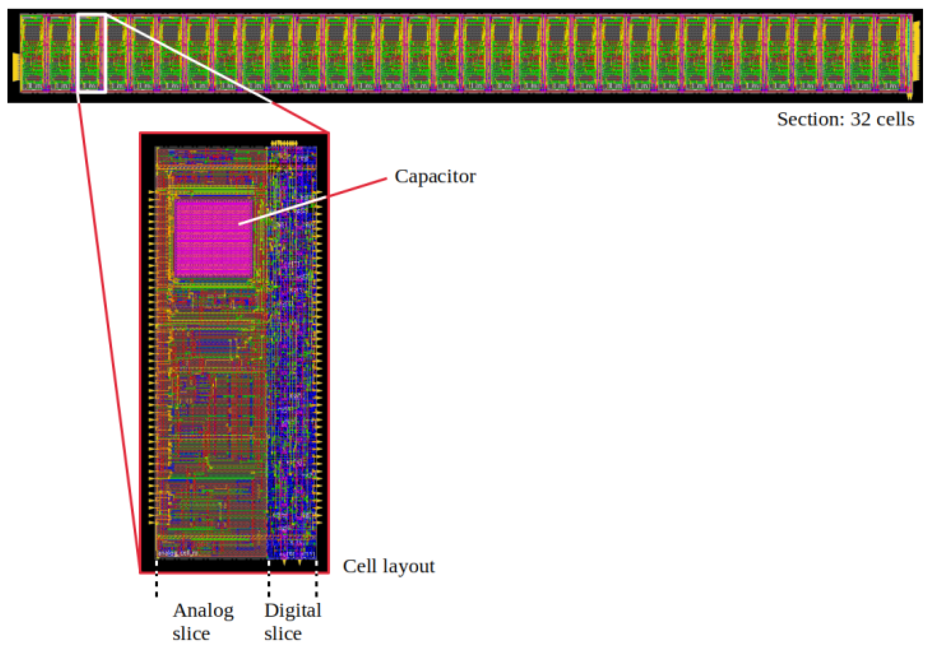
2.2. ASIC Architecture

Figure 2 shows a block diagram representation through the ASIC hierarchy. In the upper part of the image, the general partition of the ASIC is illustrated. The main digital logic is implemented in the End-Of-Column (EOC) block and in the same area, two serializers, an SPI module, and the configuration registers are located. This unit manages the configuration of the chip as well as the stages of the finite state machines (FSM) to realize the sampling, the digitization, and the readout of the data. These tasks are distributed along the 64 channels whose circuitry is schematized in the bottom part of the picture. The SiPMs induce a current signal, which is amplified by a dedicated stage. The output of the amplifier is then split between a pair of comparators and 256 cells. The first branch is used to locally generate a trigger and this information is merged into the EOC. If an event is detected, the ASIC builds a hitmap to be sent out to the FPGA and it raises a flag. In the simplest case, if the event is accepted and confirmed by the FPGA, the digital conversion can take place, as well as the readout. These steps are achieved by distributing the second branch among the array of cells. The channel can be configured to use smaller partitions of cells based on a minimum group of 32 units, which is called a section. The user can choose between 32, 64, or 256 cells operating the derandomization of the Poissonian distributed events. Indeed, in this way, the data processing involving the sampling, the conversion, and the readout can be carried out in parallel, strongly reducing the waste of time. In the blue box of Figure 2, a schematic of the analog cell is represented. Each cell is equipped with a Wilkinson ADC, which is composed of a capacitor (C) and a comparator. The capacitor stores the analog information of the signal during the sampling stage, closing S 0 and S 2 switches, and a pointer is used to control S 0 cell by cell. If the digitization is enabled, both S 0 and S 2 are opened while the bottom plate of C is connected to the output of a ramp generator with S 1 . During the data conversion, both the ramp generator and a Gray counter work with the same phase. In other terms, the output of the ramp generator is increased by the least significant bit (LSB) while the Gray counter is incremented by one at each clock cycle. When the condition V I N V B L is achieved, where V B L is a voltage threshold, the output of the comparator enables the local storage of the current Gray counter value. Another key feature of the system is the programmability of the resolution in the range between 8 bits and 12 bits. This characteristic also allows for the use of the ASIC in applications where a high granularity is not a severe requirement. Moreover, the dead time due to the digitization can be considerably reduced. However, the maximum time needed for digitizing is 2 N T c l k , where N is 12 bits and T c l k is the clock period used by the digital logic, which is equal to 5 ns because of the working frequency of 200 MHz, namely ∼20.5 μ s are required to complete the process with the nominal resolution. After the digital conversion, a data packet is available for the transmission and the dedicated serializer receives the data to build an event. The stream is composed of 8 bits for the header used for the alignment with the FPGA, 6 bits reserved for the information of the packet, 16 bits providing a timestamp, and 9 bits of address followed by the event. Because of the configurability of the parameters, the data length depends on the partition and the resolution chosen. For instance, if the user selects the 32-cells partition and a resolution of 12 bits, the total length of the data stream will be 440 bits per channel, including the headers. At ASIC level, 64 channels contribute to the event, thus this is described by 28,160 bits. Since the serializers work in double data rate at 400 MHz, in terms of time this takes slightly more than 35 μ s to transmit the entire data packet. The ASIC is designed in a commercial 65 nm CMOS technology.

Hitmap Generator

In order to reduce both the digitization and the readout times, a hitmap generator was implemented. In Figure 2, the two comparators were previously pointed out as the source of the internal triggers defining two distinct thresholds. As the point spread function of the optics has a size comparable with the pixel size, the double threshold will act in selecting both occurrences in which the spot size is localized in one pixel or distributed on more pixels. In the first case, a signal passing the high threshold in one pixel will be enough for triggering. In the other case, a lower threshold will be used for triggering, but will be conditioned to the presence of two or more nearby pixels above a low threshold. These signals are collected at the EOC level to discriminate between the cases reported in Figure 3.
(a)
The hit is concentrated into a single pixel, candidating a direct cosmic ray or a possible neutrino-event if no bi-focality is implemented in the optical system;
(b)
The event is split into two corresponding pixels in the case of a system which adopts the bi-focality to discriminate a signal from a UHECR or UHE neutrino with respect to a direct cosmic ray hit in the detector;
(c)
An event occurs at the edge of the SiPM tile, suggesting an adjacent event in the nearby tile;
(d)
A light pollution due to a city can flare a large area of the tile.
These combinations are taken into account with a dedicated FSM designed in the EOC. Each pixel has a configuration bit to set it as a core-pixel or edge-pixel. The core implements a combinatorial circuitry based on fast-OR chains to detect two or more coincidences. The edge area carried out a similar digital detector with a programmable feature. The user can select three modes for the generation of the hitmap.
  • TIME WINDOW: a time window is defined using a programmable 6-bits register with a step of 5 ns. At the end of this period, a hitmap is generated, nevertheless a physical event occurred or not;
  • HIGH THRESHOLD + COINCIDENCE + EDGE DRIVEN: the high threshold is continuously checked. If it is verified, a read hitmap request is sent to the FPGA, otherwise the coincidence condition is tested within another programmable window. If this case also fails, the pixels at the edges are monitored and a read request is generated as well;
  • FPGA REQUEST: the last mode is reserved for the active interaction with the FPGA, which can require the local generation of a hitmap. This feature results in being useful when the user wants an entire snapshot of the entire focal plane.
If the event is detected, a read request warns the FPGA that a new hitmap is available. The FPGA can reject the request, thus the FSM inside EOC comes back to a monitoring state, otherwise the signal can be accepted and the ASIC prepares the hitmap data packet for the serialization. The stream is made of 98 bits, segmented in a header part and a data part. The time required for the transmission of each hitmap is equal to ∼122 ns. If the FPGA is not responding, after an acknowledged period, the ASIC cleans its own registers and continues the sampling stage.

3. Results

The implementation of the circuitry described in the previous section was carried out using electronic design automation (EDA)/computer-aided design (CAD) tools for both the analog implementation and the digital one.
Figure 4 shows the physical implementation of a section. In the picture, the single cell unit is also magnified to highlight the analog and digital areas. The capacitor C, where the analog information coming from the SiPMs is locally stored during the sampling, is easily recognizable. On the digital side, the routing connects the 12-bits length latches dedicated to registering the digitized value to the rest of the logic. The size of a cell is 21 μ m × 56 μ m.
Table 1 reports a very preliminary estimation of the digital power. These results are obtained using the toggle rate of the behavioral simulation. The table collects the main digital blocks implemented at the channel level of hierarchy. Since, in this evaluation, the routing contribution is not considered, the final power consumption may be incremented.

4. Discussion

This section is dedicated to some considerations of the features implemented in the ASIC.
The partition of the cell array into smaller segments was adopted to derandomize the signals detected by the SiPMs. The latter are Poissonian-distributed, thus the probability of receiving n events is:
P n = μ n e μ n ! ,
where μ is the average number of events in the time window. Let us suppose we now have an event rate of 100 kHz and a dead-time of 8 μ s. This means that the probability of losing an event is:
P l o s s = 1 e 0.8 0.55 .
By changing the acquisition strategy, N segments can be used and the probability is evaluated as:
P l o s s = 1 n = 0 N μ n e μ n ! .
If N = 4 segments are considered, P l o s s would be equal to about 0.5%. This is a significant reduction compared to the 1-segment case. Moreover, another benefit derived from using sections concerns the reduced time transmission. Indeed, for short-on-time events, a smaller partition becomes convenient. This advantage is further increased by the configurability of the resolution. This feature has a direct impact on both the time conversion itself and on the data transmission. Since the conversion time depends on 2 N T c l k , where N is the number of bits and T c l k is the frequency of the clock—which is equal to 5 ns—the minimum time required for the conversion is 1.28 μ s (8 bits) and the maximum time required is ∼20.5 μ s (12 bits). These results also affect the data transmission because of the length of the words appended in the data stream. Nevertheless, several combinations are possible as well; let us consider the best and worst cases in terms of time required to complete the data sending. For the first one, a partition of 32 cells and a resolution of 8 bits are assumed. With this configuration, the transmission time in DDR takes ∼23.8 μ s considering all the data packets for 64 channels and including the headers budget. Conversely, selecting the 256-cells mode and the maximum possible resolution of 12 bits, the same process requires ∼249 μ s. Finally, an estimation of the total time required by the conversion and the data readout in the two cases is possible. In the first configuration, the system takes slightly more than 25 μ s to complete these tasks, while in the second case, ∼270 μ s are needed. Naturally, the cross combinations between segmentation and resolution define a trade-off that must be evaluated considering the application requirements.

5. Conclusions

In the context of UHECR and UHE neutrino astronomy, a 64-channel ASIC for an SiPMs readout carried out in a commercial 65 nm CMOS technology has been described. The chip is designed to be interfaced with a 8 × 8 pixel matrix, providing a hitmap to an FPGA for preliminary pattern recognition. A channel can be partitioned into sections of 32, 64, or 256 cells to derandomize the signal at 200 MHz. The main benefit of this architecture is a considerable saving of time during the processing of the data. Another key feature is represented by the configurability of the resolution in the interval 8–12 bits. The readout is realized with two dedicated serializers, one reserved to the hitmap and the other to the data. The serializers work at 400 MHz in the double data rate and the data stream sent out to the FPGA has a variable length according to the parameters selected during the configuration of the ASIC.

Author Contributions

Conceptualization, A.D.S., M.E.B. and A.R.; methodology, A.D.S., S.G. and A.R.; software, A.D.S., S.G., M.M., S.C.Z. and P.A.P.; validation, A.R.; investigation, A.D.S., S.G., M.M., S.C.Z. and P.A.P.; resources, M.E.B. and A.R.; data curation, A.D.S., M.M. and P.A.P.; writing—original draft preparation, A.D.S.; writing—review and editing, A.D.S. and M.E.B.; visualization, A.D.S. and M.M.; supervision, A.D.S. and M.E.B.; project administration, M.E.B. and A.R.; funding acquisition, M.E.B. All authors have read and agreed to the published version of the manuscript.

Funding

The front-end electronics described in this paper are part of the development performed within the ASI-INFN agreement for EUSO-SPB2 n.2021-8-HH.0 and its amendments.

Conflicts of Interest

The authors declare no conflict of interest.

References

  1. Eser, J.; Olinto, A.V.; Wiencke, L. Overview and First Results of EUSO-SPB2. In Proceedings of the 38th International Cosmic Ray Conference (ICRC2023), Nagoya, Japan, 26 July–3 August 2023; Volume 444. [Google Scholar]
  2. Burmistrov, L. NUSES Collaboration. Terzina on board NUSES: A pathfinder for EAS Cherenkov Light Detection from space. arXiv 2023, arXiv:2304.11992. [Google Scholar]
  3. Olinto, A.V.; Krizmanic, J.; Adams, J.H.; Aloisio, R.; Anchordoqui, L.A.; Anzalone, A.; Bagheri, M.; Barghini, D.; Battisti, M.; Bergman, D.R.; et al. The POEMMA (Probe of Extreme Multi-Messenger Astrophysics) observatory. J. Cosmol. Astropart. Phys. 2021, 2021, 007. [Google Scholar] [CrossRef]
  4. De Mitri, I.; Di Santo, M. The NUSES space mission. J. Phys. Conf. Ser. 2023, 2429, 012007. [Google Scholar] [CrossRef]
  5. De Mitri, I.; Di Santo, M. The Ziré instrument on board the NUSES space mission. In Proceedings of the 38th International Cosmic Ray Conference (ICRC2023), Nagoya, Japan, 26 July–3 August 2023; Volume 139. [Google Scholar]
  6. Tedesco, S.; Di Salvo, A.; Rivetti, A.; Bertaina, M. A 64-channel waveform sampling ASIC for SiPM in space-born applications. J. Instrum. 2023, 18, C02022. [Google Scholar] [CrossRef]
Figure 1. (a) Block diagram of a tower-like structure formed by the SiPMs plane and the ASICs board, (b) layout of the design where the red square is a SiPM tile used as reference.
Instruments 07 00050 g001
Figure 2. Block diagram representation of the ASIC, a channel (red box), and a cell (blue box).
Instruments 07 00050 g002
Figure 3. Possible hitmaps configurations: (a) single pixel, (b) coincidence, (c) edge-pixel and (d) light pollution where the orange area indicates the core-pixels, the blue regions illustrate the edge-pixels and the red boxes show the hit pixels.
Instruments 07 00050 g003
Figure 4. Layout of a section and schematic view of a cell.
Instruments 07 00050 g004
Table 1. Power estimation for the digital blocks integrated into the channel. The leftmost two columns refer to the power and area of a single block, N indicates the number of units, and the rightmost two columns report the total power and area, respectively.
BlockPowerAreaNPower T Area T
( μ W)( μ m 2 ) ( μ W)( μ m 2 )
Cell 2.5 352256 640.0 90 , 225
Section 2.5 968 20.0 772
Section controller 31.4 8404 125.4 3360
Gray counter 42.4 3761 42.4 376
Gray decoder 2.9 3571 2.9 357
Channel controller 430.0 80831 430.0 8083
Total 1260.7 103 , 173
Disclaimer/Publisher’s Note: The statements, opinions and data contained in all publications are solely those of the individual author(s) and contributor(s) and not of MDPI and/or the editor(s). MDPI and/or the editor(s) disclaim responsibility for any injury to people or property resulting from any ideas, methods, instructions or products referred to in the content.

