Article

A Rapid, Non-Destructive Method to Detect Counterfeit Integrated Circuits Using a Resonant Cavity System

Department of Electrical and Computer Engineering, The Ohio State University, Columbus, OH 43210, USA
*
Author to whom correspondence should be addressed.
Instruments 2024, 8(3), 37; https://doi.org/10.3390/instruments8030037
Submission received: 1 May 2024 / Revised: 9 June 2024 / Accepted: 5 July 2024 / Published: 7 July 2024

Abstract

:
The counterfeiting of integrated circuits (ICs) has been a growing issue. Current available methods used to detect counterfeit ICs can be expensive, imprecise, and time-consuming. This paper explores the resonant cavity system: a non-contact, non-destructive method to rapidly differentiate counterfeit ICs from authentic ones. The system captures a unique signature of an IC placed inside it. Data were captured for ICs of various technologies and authenticities. The data included return loss values captured at various transverse electric (TE) modes between 2.8 GHz and 6 GHz. This allowed for the comparison of the effectiveness of the various TE modes in being able to distinguish ICs. The resonant cavity system was able to distinguish most of the ICs at higher TE modes.

1. Introduction

1.1. Background

The advent of integrated circuits (ICs) revolutionized the world of electronics. Today, integrated circuits are incorporated in everyday household appliances, such as microwaves, smart thermostats, and smart phones, as well as critical systems and infrastructures in the defense industry, such as missile guidance systems, satellites, and fighter jets. Counterfeiters have taken advantage of the high demand for ICs to create counterfeit versions. These counterfeit ICs are then sold as authentic parts for fractions of authentic IC prices. Businesses that are no longer able to obtain their ICs via reputable sources are turning to dubious, unknown sellers on the internet to obtain out-of-stock or obsolete parts. Ordering ICs from these unknown sources greatly increases the risk of receiving counterfeit ICs. There is, hence, a growing need to remove the risk of counterfeit parts in an efficient, rapid, cost-effective, and non-destructive manner.
“Counterfeit ICs” is a broad term used to describe ICs of several types. Some of these include recycled, remarked, overproduced, defective, cloned, and tampered ICs. The most common types of counterfeit ICs are recycled and remarked ICs. It is reported that 80 percent of counterfeit ICs are either recycled or remarked [1]. Recycled and remarked ICs can be hard to distinguish since they can look identical to authentic ICs on the outside. Furthermore, recycled ICs can functionally perform similarly to authentic ICs since they sometimes consist of repackaged authentic IC dies.
In previous works [2,3,4], a resonant cavity with cavity dimensions of 7 cm × 2.9 cm × 3.7 cm was used. The resonant cavity used in this paper is slightly larger (11.19 cm × 2.79 cm × 5.58 cm). The shape and larger cavity size allowed for the collection of data at multiple transverse electric (TE) modes since there is less overlap among the resonant frequencies peaks at higher TE modes compared to the smaller resonant cavity. In [2], a resonant cavity system that can distinguish ICs of various package types, authenticity, and technology was developed. The system used a signature of reflection coefficient values ranging between 10 GHz and 19 GHz using 60,003 points. Similarly, a frequency band between 10 GHz and 40 GHz using 100,000 points was used in other works [3,4]. In [3], the system proved capable of detecting tampered ICs. In [4], the resonant cavity system was used in combination with a Fourier transform infrared spectroscopy (FTIR) system. The combination of the resonant cavity and FTIR system, allowed for the improved detection of a variety of counterfeit ICs, such as remarked ICs, where the difference can mostly lie in the subtle material differences in the packaging.
This paper uses the return loss along with the frequency values of the resonant frequency peak at five specific TE modes. This allowed for the analysis and comparison of the efficacy of each specific TE mode. Furthermore, the resonant cavity system used in this paper used signature values between 2.8 GHz and 6 GHz, which is substantially lower than the frequency band used previously. The groups of ICs tested included authentic and suspect counterfeit versions of the ICs.
The unique features of the method can be summarized as follows.
  • We propose a rapid, low-cost, non-contact, non-destructive approach to differentiate an IC by its part number and authenticity based on the scattering parameters (S-parameters) obtained when the IC is placed inside a resonant cavity.
  • The S-parameters obtained create a unique signature based on the structural layout (package, pad, pin, wire bond, and die structure) and functionality of the silicon die.
  • The method can be applied to any IC regardless of technology type (analog, digital, mixed-signal), package (dual in-line package (DIP), quad flat no-leads (QFN), etc.), size (small, medium, large), or state (obsolete, active, new) without the need of any modification pre- or post-fabrication.
  • The method only requires unique structures to precisely hold and place specific package types inside the resonant cavity.
  • The method does not require access to the pins of the ICs.
  • The system uses the S-parameters as quantitative metrics, thus eliminating the need for subject matter experts to operate the system. Unlike traditional techniques, such as visual inspection and X-ray radiography, which typically rely on qualitative assessments by experts, the resonant cavity system provides faster and more objective results based on measurable differences in the signatures.

1.2. Counterfeit Detection Methods

1.2.1. Physical Inspections

Physical inspections are performed to examine the physical and material properties of an IC. Some common physical inspection methods include external visual inspection (EVI) and X-ray imaging [5,6]. In EVI, the exterior structure of the IC is inspected thoroughly with the use of a low-power microscope. X-ray imaging is used to inspect the internal structure of the IC. While these methods can be effective in detecting counterfeit ICs, they can be very expensive. EVI can also be time-consuming and imprecise since it only examines the exterior of the IC, which can easily be replicated by counterfeiters. X-ray imaging is also known to have adverse effects on certain types of ICs [7,8,9,10].

1.2.2. Electrical Inspections

Electrical inspections examine the electrical and functional properties of the IC. Common electrical inspections include parametric tests and functional tests. Parametric tests measure the AC and DC parameters of an IC [11,12]. Functional tests are efficient in verifying the functionality of a component. Functional tests can also determine whether certain ICs are designed with different technologies. However, electrical inspections are ineffective when distinguishing sophisticated cloned ICs [13].

1.2.3. Side-Channel Analysis

Side-channel analysis (SCA) is a powerful technique used to exploit the unintended physical emissions or side effects of a device to extract sensitive information. SCA leverages observable side effects, such as power consumption, electromagnetic emissions, sound, or backscattering. These side effects, or “side-channels”, can reveal detailed information about the internal operations of a device, thereby enabling attackers to circumvent access controls and protections. On the other hand, defenders can utilize SCA to detect anomalies and intrusions by monitoring these side effects and identifying deviations from normal behavior.
Each SCA technique offers its advantages and disadvantages [14]. Backscattering side-channel analysis is relatively new and involves monitoring the impedance changes in switching circuits [15]. These changes occur as transistors in digital logic gates switch between high and low states, modulating and reflecting an injected carrier signal. This method boasts high bandwidth, the ability to increase signal strength when needed, frequency shifting to avoid noise and interference, and more accurate focus on specific chip parts. However, its complexity in implementation is a notable drawback. Electromagnetic (EM) side-channel analysis captures the electromagnetic waves emitted by a device during operation, which vary with the current flow in the device’s circuits [16]. While it offers high bandwidth and the ability to monitor devices from a distance, the signal strength varies greatly between devices, and the range is limited by the radiation magnitude. Furthermore, its signal-to-noise ratio is affected by noise and interference. Power side-channel analysis, based on monitoring a device’s power consumption to infer its internal operations, provides a direct correlation with device activity and can be highly informative with precise measurements [17,18]. Nonetheless, it requires a direct connection to the device and has limited bandwidth due to on-chip mechanisms that filter power fluctuations. A common drawback among all SCA techniques is the requirement for access to the pins of the IC. Additionally, these techniques often necessitate powering on or biasing the IC to generate the side-channel signals. Hence, they require specific setups based on the part type to probe the pins of the ICs. This incurs additional cost and time for development.

1.2.4. Microwave Techniques

Microwave techniques similar to the resonant cavity system that uses S-parameters to distinguish ICs have also been used in the past. For example, Shinde et al. [19] used an open-ended rectangular waveguide aperture to rapidly detect dissimilar and aged ICs. An advantage of these methods is that they do not require access to the pins of the IC, nor do they require the IC to be powered on or biased. A drawback of the resonant cavity system is its sensitivity to the placement position of the IC and manufacturing or process variations. While the resonant cavity system is highly effective at detecting minor circuit variations [3], it may face difficulties in identifying extremely subtle alterations or those obscured by inherent manufacturing inconsistencies. Variations within acceptable tolerances or those stemming from wafer process variations can be hard to distinguish from deliberate tampering. Similarly, differentiating between pristine ICs and aged ICs—especially when both are manufactured using the same die revision and packaging—can be challenging, as the subtle effects of aging may be masked by these inherent inconsistencies. Consequently, the effectiveness and resolution of the resonant cavity system can vary depending on the specific manufacturing and process variations of the IC.

1.2.5. Chip and Package ID

Chip or package IDs can be used to uniquely identify ICs. Chip IDs, such as physical unclonable functions (PUFs) [20,21], can be implemented on dies during or after fabrication. PUFs utilize the random variations in the IC manufacturing process to generate a unique signature for each IC [22]. The downside of this method is that, in most cases, it requires additional costs and overhead on the IC die. Furthermore, chip IDs can only be implemented on new ICs. Package IDs, such as DNA markings [23], nanorods [24], and magnetic PUFs [25], can be used to tag active and obsolete components.

1.3. Resonant Cavity

1.3.1. Description and Applications

The cavity is essentially a hollow, closed metal box. The resonant cavity used in these experiments is rectangular and is coupled with a sub-miniature version A (SMA) probe that is inserted through a hole in the top of the cavity wall. When the cavity is excited by radio waves through the probe, resonant modes are formed, corresponding to the field variations inside the cavity structure. The resonant modes formed are either transverse electric or transverse magnetic (TM) modes that are based on the orientation of the electric or magnetic field vectors corresponding to the direction of propagation. At these resonant frequency values, the moving radio waves form standing waves, resulting in a high return loss (4). Resonant cavities have been used in a variety of applications in the past, including filters, oscillators, and frequency meters. They have also been used to measure the dielectric properties of materials as far back as 1944 [26]. Recently, resonant cavities have been used as near-field scanning microwave microscopes (NSMM). These systems can have nanoscale spatial resolutions [27] and have demonstrated the ability to characterize semiconductor structures [28].

1.3.2. Resonant Frequencies

The resonant frequencies of a rectangular cavity can be determined based on its geometry, assuming the cavity is empty and lossless. The dimensions of the cavity are denoted as a, b, and d, which correspond to the width, height, and length of the cavity, respectively, as illustrated in Figure 1. The resonant modes are characterized by the indices m, n, and p, which represent the mode numbers in the x, y, and z directions, respectively. The speed of light in a vacuum is represented by c.
The wave modes in a resonant cavity are specific patterns of the electromagnetic fields that satisfy the boundary conditions imposed by the cavity’s walls [29]. These modes are quantized, meaning only certain discrete frequencies resonate within the cavity. Each mode is defined by three integers m, n, and p, which indicate the number of half-wavelengths along the x, y, and z axes, respectively. These integers must be positive whole numbers or zero, with at least one of them being non-zero, to represent a valid mode. The resonant frequency can be calculated for a given mode (1). The accuracy of these calculations is based on the assumption that the cavity is perfectly empty and lossless, meaning it does not contain any materials that can absorb or dissipate energy.
Resonant Frequency ( f m n p ) = c 2 π m π a 2 + n π b 2 + p π c 2

1.3.3. Perturbation Equations

When an object is placed inside the cavity, the resonant frequency value is shifted based on the dielectric properties and shape of the inserted object. This shift in frequency can be approximated using the perturbation method, which assumes that the actual fields of a cavity with a small shape or material perturbation are not greatly different from those of the unperturbed cavity. To demonstrate the effects of material and shape perturbations, two examples are used [29].
For material perturbation, assume a thin dielectric slab with relative permittivity ϵ r is inserted into the bottom of the cavity, as seen in Figure 1a. Assuming ω 0 is the dominant resonant frequency of the original cavity and ω is the resonant frequency of the perturbed cavity, the fractional change in the dominant resonant frequency can then be derived as seen in (2).
For shape perturbation, assume a thin screw with radius r 0 and height l is inserted into the cavity, as seen in Figure 1b. The fractional change in the dominant resonant frequency can then be derived as seen in (3).
From Equations (2) and (3), it can be concluded that objects of higher permittivity and larger dimensions are going to incur larger shifts in the resonant frequency values. Furthermore, the position of the object inside the cavity can influence the amount of shift in resonant frequency value since the specific position of the object inside the cavity modifies the inner structure of the cavity in a different way.
ω ω 0 ω 0 = ( ϵ r 1 ) t 2 b
ω ω 0 ω 0 = 2 l π r 0 2 a b d

1.4. Return Loss

The return loss (4) represents the ratio of the incident power ( P i ) to the reflected power ( P r ). It is expressed as a ratio in decibels (dB), where P i denotes the power of the incoming signal incident on the cavity and P r represents the power of the signal reflected back from the cavity. At the resonant frequency, the amount of reflected power ( P r ) is minimized, which results in a large positive return loss value. This indicates that most of the incident power is absorbed by the cavity rather than being reflected. The return loss can also be interpreted as a measure of the input impedance of the resonant cavity. At resonance, this input impedance is typically real and can be considered purely resistive.
The exact value of the return loss at each resonant frequency depends on several factors, including the matching of the cavity to the characteristic impedance of the attached input cable, the resistivity of the cavity walls, and the dielectric properties of the cavity or any objects within it.
Return Loss ( dB ) = 10 log 10 P i P r

1.5. IC EM Signature

As demonstrated with the perturbation equations, the resonant frequencies of the resonant cavity shift based on the shape and material properties of any object inserted inside it. Hence, if the shift in the resonant frequency and return loss values are captured at multiple modes, these values can create a unique signature that can be used to uniquely identify an object. This principle can, hence, be applied to ICs. When an IC of the same part number is consistently placed inside a resonant cavity at the same position, the IC should theoretically shift the resonant frequency by the same amount for ICs of the same part number. This is assuming ICs of the same part number have the same external and internal structure. In some rare cases, authentic ICs can suffer from inconsistencies in their structure because of manufacturing inconsistencies and defects. If a counterfeit IC is placed in the same position inside the cavity, the resonant frequency will theoretically shift a different amount since the shape and dielectric properties of the counterfeit IC are very different compared to that of authentic versions. This is, in part, due to the large differences seen in the interior of counterfeit ICs, such as their die and lead frame structure. Hence, for a counterfeit IC to replicate the EM signature of an authentic IC, it has to match its internal and external structure with high accuracy, which is a much more challenging and costly task for counterfeiters than merely replicating the exterior of the authentic IC.

1.6. Design

The resonant cavity used in this paper has exterior dimensions of 14.2 cm × 5.03 cm × 7.57 cm. The resonant cavity is constructed using Aluminum 6061 with an SMA probe inserted through the top of the cavity wall. The inner cavity has dimensions of 11.19 cm × 2.79 cm × 5.58 cm. Using the dimensions of the inner cavity along with the mode numbers (m, n, p), the resonant frequencies for the first five TE modes can be calculated using (1); the resonant cavity theoretically consists of a fundamental frequency, TE101 mode at 3.00 GHz, TE102 mode at 3.79 GHz, TE103 mode at 4.83 GHz, TE104 mode at 5.99 GHz, and TE201 mode at 5.53 GHz.

2. Materials and Methods

2.1. Setup and IC Placement

To collect the resonant frequency and return loss values of each IC, the resonant cavity was first connected to the vector network analyzer (VNA). The IC was then carefully placed inside the resonant cavity by inserting the IC into a plastic holder, which was placed on a plastic platform (Figure 2b). The plastic holder and platform were custom-made using a 3D printer and 3D design software (AutoCAD 2025.0.1 V.72.0.0). The plastic holder held the IC in place and was placed onto the platform. Placement consistency was vital for acquiring consistent measurements. Any deviations in the placement of the IC onto the holder or inside the cavity could cause inconsistencies in the measurements. Hence, the platform was designed to fit snugly inside the resonant cavity to maximize the placement consistency of the IC inside the cavity. Once the IC was placed inside the cavity, the resonant cavity was closed with its lid. The lid was then tightened using four hex bolts and nuts in the four corners of the rectangular lid.

2.2. Measurement

The return loss values were then recorded between 2.8 and 6 GHz for 100,000 points using an intermediate frequency bandwidth of 10 kHz. The power level used for the measurements was −10 dBm. The measurement for each IC sample was taken once and not repeated. While the initial S-parameter data consisted of 100,000 points, the data were later processed to extract only the resonant frequency and return loss values at the five TE modes.

2.3. Dataset

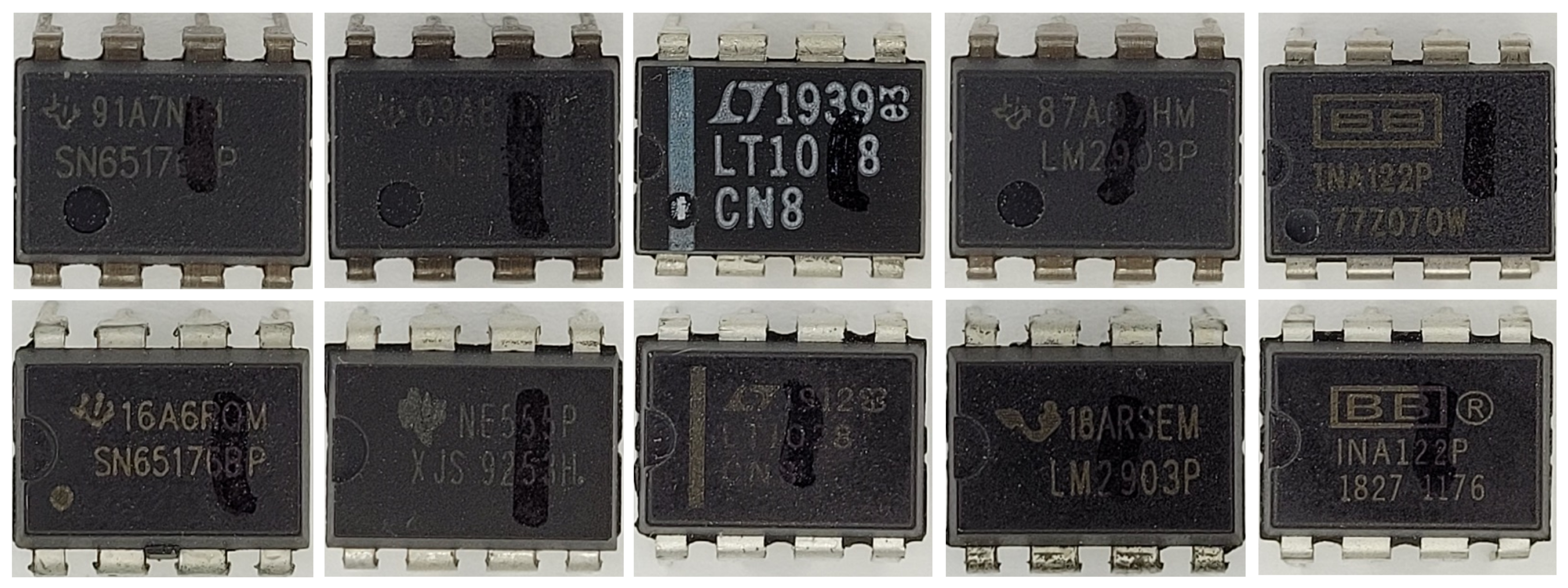
The ICs used in this paper consisted of two types: authentic and suspect counterfeit ICs. Five authentic IC part numbers and their corresponding suspect counterfeit versions were used for this experiment (Figure 3). The description of each IC used is summarized in Table 1. For each part number, 5 IC samples were used. In total, 50 IC samples were used for this experiment. The authentic ICs were sourced from reputable sources, while their suspect counterfeit versions were obtained through non-reputable third-party sellers for a fraction of the price of the authentic parts.
The G-19 Counterfeit Electronic Parts Committee of SAE International [30] has created multiple industry standards for the detection and mitigation of counterfeit electronic parts. The latest standard for the detection of counterfeit electronic parts, AS6171A [31], describes EVI methods in document AS6171/2A [32]. Method A and Method B consist of various procedures for general and detailed EVI. Using these procedures on our samples, various discrepancies were found in the suspect counterfeit ICs, including incorrect logos, inconsistent text alignment, poor ink quality, and corrosion on the leads. The significant discrepancies identified using the EVI methods described in AS6171A, combined with the low price at which the suspect ICs were acquired, led to the conclusion that these ICs were likely counterfeit. However, since it is nearly impossible to determine the authenticity of an IC with absolute certainty, these ICs are referred to as “suspect” or “suspect counterfeit” ICs in this paper.

3. Results

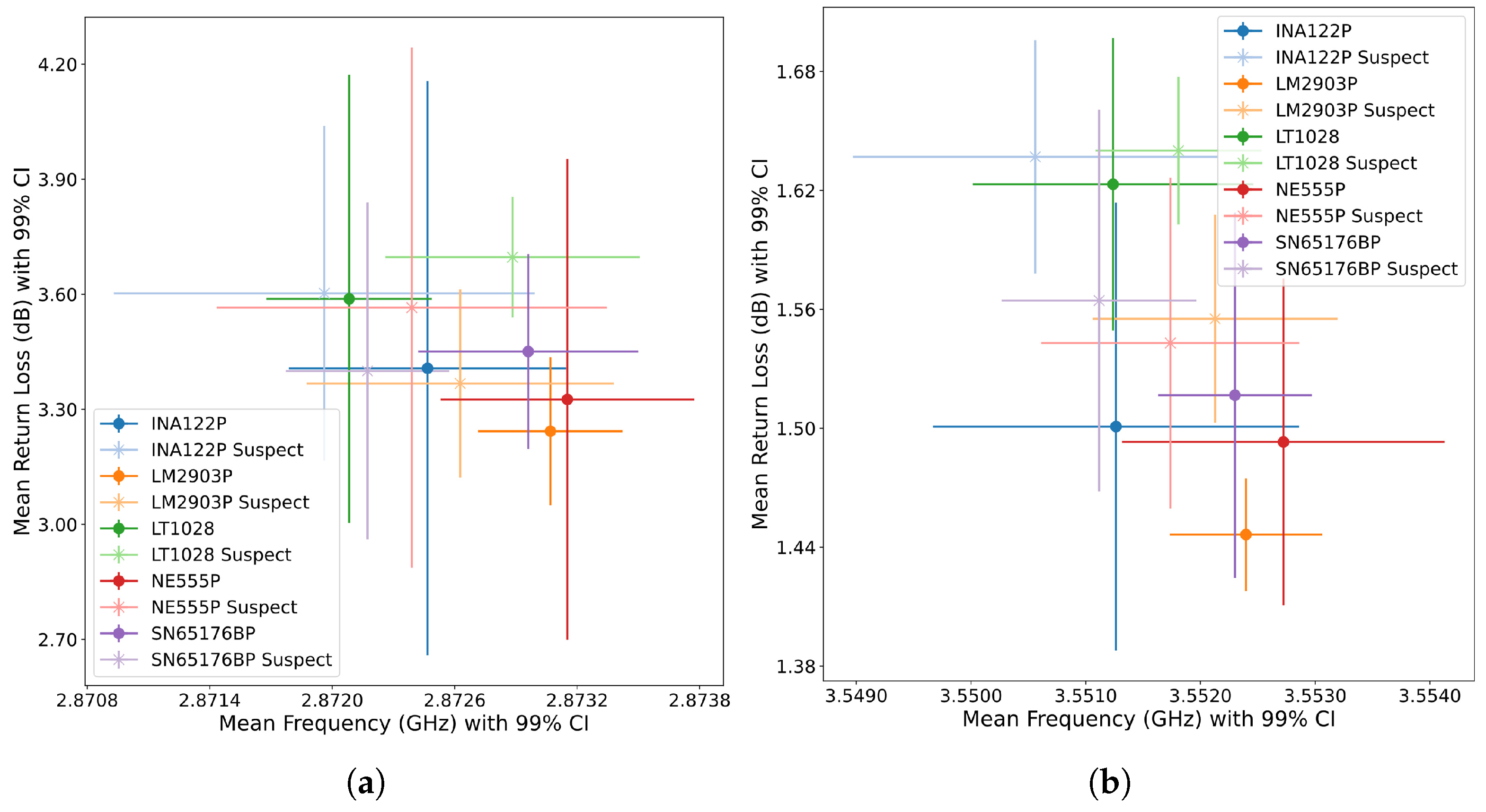
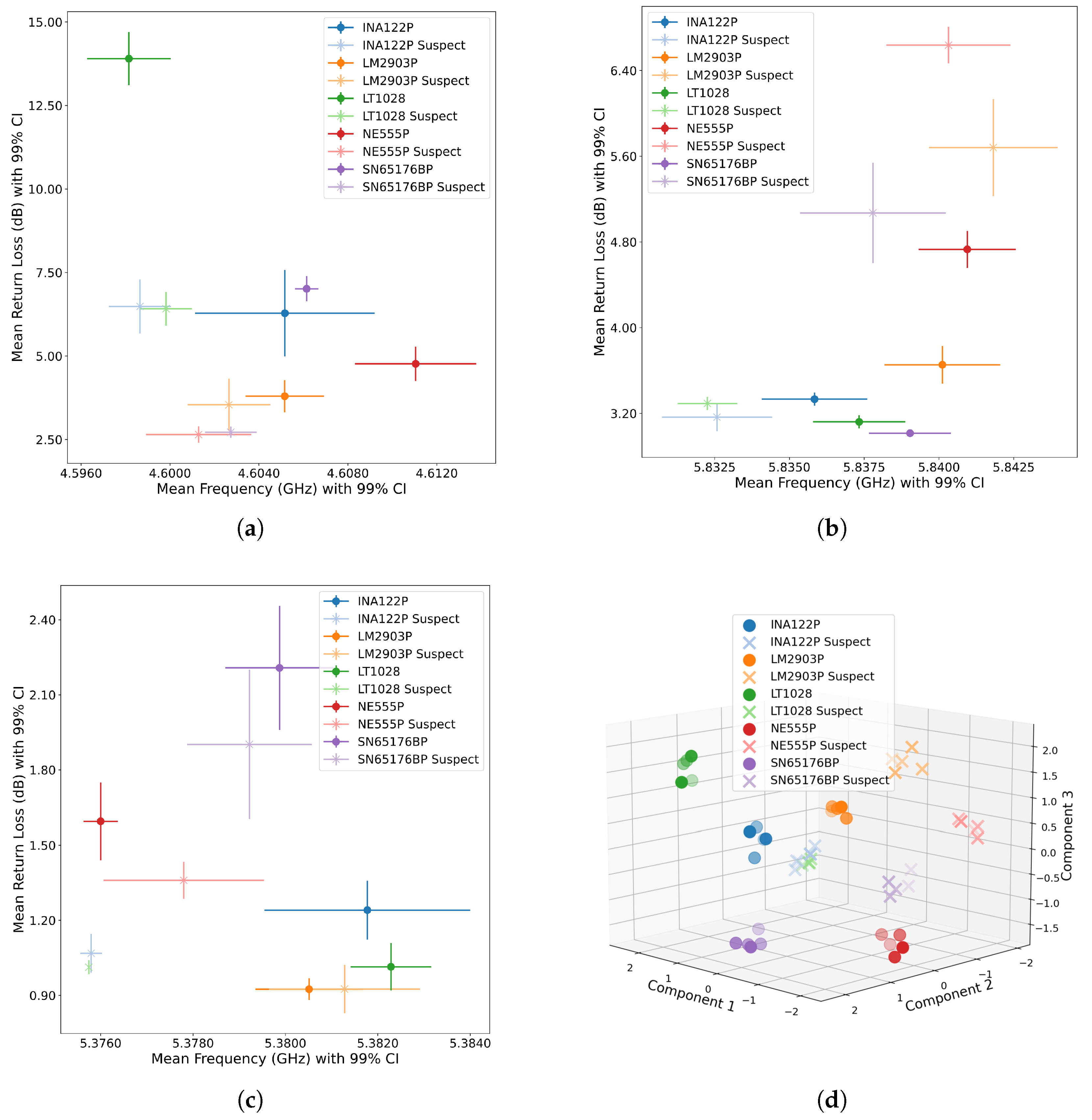
The data collected from the VNA can be visually analyzed by plotting the return loss values over the resonant frequency for the corresponding TE mode. Five IC samples were used for each IC part number. An error bar is used to plot these values (Figure 4 and Figure 5). The error bar includes the sample mean ( x ¯ ) value, denoted by the “o” marking for the authentic samples and the “x” marking for the suspect counterfeit samples. The 99% confidence interval (CI), derived using the Student’s t-distribution, is denoted by the horizontal and vertical bars of the five samples of each IC. The results of the error plots show a 99% confidence interval, indicating that we can be 99% confident that the true mean lies within this interval. If the confidence intervals of two sample populations (ICs) do not overlap, we know that they are statistically different. This confidence interval is calculated using the Student’s t-distribution, appropriate for our small sample size ( n = 5 ). The calculation is performed as follows:
  • Calculate the sample mean ( x ¯ ):
    x ¯ = 1 n i = 1 n x i
  • Calculate the sample standard deviation (s):
    s = 1 n 1 i = 1 n x i x ¯ 2
  • Determine the t-score for 99% confidence and n 1 degrees of freedom ( t 0.005 , n 1 ) from the t-distribution table.
  • Calculate the margin of error ( M E ):
    M E = t 0.005 , n 1 × s n
  • Determine the confidence interval ( C I ):
    C I = ( x ¯ M E , x ¯ + M E )
Note that the scales on the axes are not consistent among all the graphs. It is immediately noticeable that there is significant overlap in the TE101 (Figure 4a) and TE102 (Figure 4b) modes; however, the values of the ICs do not overlap as much in the TE103 (Figure 5a), TE104 (Figure 5b), and TE201 (Figure 5c) modes.
Principal component analysis (PCA) was then performed on the values obtained at the TE103, TE104, and TE201 modes [33]. For each mode, two values were extracted—the resonant frequency and the return loss—resulting in a total of six values per IC sample. PCA was used to reduce these six values to three principal components, which summarize the most significant variations in the data while retaining the primary effects of the original features. This was achieved by transforming the original variables into new, uncorrelated variables (principal components) that were linear combinations of the original variables [34]. The first principal component accounts for the largest possible variance in the data, the second principal component accounts for the second largest variance orthogonal to the first, and so on. This dimensionality reduction allowed for visualization in a three-dimensional plot (Figure 5d), making it easier to identify patterns and differences between the authentic and suspect counterfeit ICs. Before applying PCA, the features were standardized to a standard score (z), calculated by subtracting the mean ( μ ) of each feature and dividing by its standard deviation ( σ ), as shown in (9). This standardization ensured that each feature contributed equally to the analysis, preventing any single feature from disproportionately influencing the results.
Standard score ( z ) = ( x μ ) σ

4. Discussion

The unique clustering of the resonant frequency and return loss values based on the part type of the ICs in the higher TE modes suggests that the higher TE modes are relatively more efficient in differentiating IC part numbers compared to the lower TE modes. It is possible that the higher frequencies can differentiate ICs at a higher resolution since higher frequencies have relatively shorter wavelengths. It is also possible that the higher TE modes are more sensitive to perturbations because of the presence of higher half-wave patterns compared to the lower TE modes. Using PCA and combining the parameters obtained in the TE103, TE104, and TE 201 modes showed that the part numbers form unique clusters with the exception of the suspect counterfeit INA122P and suspect counterfeit LT1028 parts (Figure 5d). It is possible that counterfeiters may be using identical chips and packages for these two IC parts. It is also possible that the method may be lacking in resolution and, hence, unable to identify the differences. Further extensive physical and electrical inspections need to be conducted to verify this.
The suspect counterfeit IC samples have a higher variance among their IC samples compared to the authentic ICs. This large variance can be attributed to the inconsistent manufacturing process and/or variance of types of parts (cloned, recycled, defective, empty) in each suspect counterfeit IC batch. Even though suspect counterfeit ICs have a larger variance in their metrics compared to authentic ICs, there still exist some large variances in some authentic samples as well. This can be the result of such anomalies. Another drawback of the method is that the specific differences in the structure of the IC remain unknown. While it is likely possible to differentiate the ICs used in this experiment using just the values obtained at the higher TE modes, this method may not be as effective in telling apart smaller footprint ICs with smaller variations among them. For instance, distinguishing tampered ICs where the changes between the baseline, non-tampered version and tampered version are minute requires the use of the entire signature at even higher frequencies [3]. The need to precisely place the IC inside the cavity is another disadvantage of the system. While this can be combated with the use of a custom holder, the additional time spent on precise placement makes the method less efficient. However, this can be addressed in the future with the incorporation of precise, automated pick-and-place robots. The incorporation of automated pick-and-place robots can greatly enhance the speed at which measurements are gathered. Modifications such as using a spring-loaded design to open and close the lid or the use of a partially open cavity can also be made to further improve the speed of measurements. Batch testing, where multiple IC signatures are collected at once, can also theoretically be implemented to enhance speed.

5. Conclusions

A system that can distinguish ICs with high precision based on their part numbers and authenticity is developed. A comparison is made between lower and higher TE modes. The method proves to be advantageous for rapidly and efficiently distinguishing ICs in a cost-efficient manner compared to more expensive imaging systems, such as X-ray. A major advantage of this system is that it can be applied to any IC type or package without the need for any modification to the IC or knowledge of the IC layout. The method’s inability to produce an image of the IC layout and only a signature is, however, a disadvantage. While the resolution of the resonant cavity used in this paper proved to be sufficient for distinguishing DIP-8 ICs, higher frequencies and additional data points are required when distinguishing ICs of smaller footprints or when trying to distinguish minute variations.

Author Contributions

Conceptualization, A.N., R.L. and G.C.; methodology, A.N., R.L. and G.C.; software, A.N.; validation, A.N., R.L. and G.C.; formal analysis, A.N., R.L. and G.C.; investigation, A.N.; resources, A.N., R.L. and G.C.; data curation, A.N.; writing—original draft preparation, A.N.; writing—review and editing, A.N., R.L. and G.C.; visualization, A.N.; supervision, A.N., R.L. and G.C.; project administration, A.N., R.L. and G.C.; funding acquisition, R.L. All authors have read and agreed to the published version of the manuscript.

Funding

This research was funded by the Air Force Research Laboratory under grant number FA8650-19-1-1741.

Institutional Review Board Statement

Not applicable.

Informed Consent Statement

Not applicable.

Data Availability Statement

The data presented in this study are available upon request from the corresponding author.

Conflicts of Interest

The authors declare no conflicts of interest. The funders had no role in the design of the study; in the collection, analyses, or interpretation of data; in the writing of the manuscript; or in the decision to publish the results.

References

  1. Guin, U.; Dimase, D.; Tehranipoor, M. Counterfeit Integrated Circuits: Detection, Avoidance, and the Challenges Ahead. J. Electron. Test. 2014, 30, 9–23. [Google Scholar] [CrossRef]
  2. Nechiyil, A.; Lee, R.; Chapman, G. Detection of Anomalous Integrated Circuits Using a Cavity Resonator System with Machine Learning. In Proceedings of the 2021 IEEE Physical Assurance and Inspection of Electronics (PAINE), Washington, DC, USA, 30 November–2 December 2021; pp. 1–7. [Google Scholar] [CrossRef]
  3. Nechiyil, A.; Lee, R.; Chapman, G.; McCue, J.J. Benchmarking ResCav—A Resonant Cavity System Used to Detect Counterfeit Microelectronics. In Proceedings of the 49th International Symposium for Testing and Failure Analysis, Phoenix, AZ, USA, 12–16 November 2023; pp. 131–135. [Google Scholar] [CrossRef]
  4. Nechiyil, A.; Xi, C.; Asadizanjani, N.; Lee, R.; Chapman, G. Evaluating a Multi-modal, Non-destructive Approach Combining a Resonant Cavity System and Infrared Spectroscopy to Detect Counterfeit and Anomalous Integrated Circuits. IEEE Trans. Components Packag. Manuf. Technol. 2024. [Google Scholar] [CrossRef]
  5. Mahmood, K.; Carmona, P.L.; Shahbazmohamadi, S.; Pla, F.; Javidi, B. Real-time automated counterfeit integrated circuit detection using x-ray microscopy. Appl. Opt. 2015, 54, D25–D32. [Google Scholar] [CrossRef]
  6. Ahmadi, B.; Heredia, R.; Shahbazmohamadi, S.; Shahbazi, Z. Non-destructive automatic die-level defect detection of counterfeit microelectronics using machine vision. Microelectron. Reliab. 2020, 114, 113893. [Google Scholar] [CrossRef]
  7. Dogan, H.; Alam, M.M.; Asadizanjani, N.; Shahbazmohamadi, S.; Forte, D.; Tehranipoor, M. Analyzing the Impact of X-ray Tomography on the Reliability of Integrated Circuits. In Proceedings of the 41st International Symposium for Testing and Failure Analysis, Portland, OR, USA, 1–5 November 2015; pp. 154–163. [Google Scholar] [CrossRef]
  8. Alam, M.; Shen, H.; Asadizanjani, N.; Tehranipoor, M.; Forte, D. Impact of X-Ray Tomography on the Reliability of Integrated Circuits. IEEE Trans. Device Mater. Reliab. 2017, 17, 59–68. [Google Scholar] [CrossRef]
  9. Barnaby, H.J. Total-Ionizing-Dose Effects in Modern CMOS Technologies. IEEE Trans. Nucl. Sci. 2006, 53, 3103–3121. [Google Scholar] [CrossRef]
  10. Ma, T.; Dressendorfer, P. Ionizing Radiation Effects in MOS Devices and Circuits; A Wiley-Interscience Publication, Wiley: Hoboken, NJ, USA, 1989. [Google Scholar]
  11. Parametric tests meet the challenge of high-density ICs: G. F. Nelson and W. F. Boggs. Electronics p. 108 (Dec. 1975). Microelectron. Reliab. 1976, 15, 177. [CrossRef]
  12. Soma, M. Fault coverage of DC parametric tests for embedded analog amplifiers. In Proceedings of the IEEE International Test Conference-(ITC), Baltimore, MD, USA, 17–21 October 1993; pp. 566–573. [Google Scholar] [CrossRef]
  13. Sharpe, T. Functional Electronic Clones—The Most Dangerous New Counterfeit Threat Facing the Entire Electronics Industry Today. In Proceedings of the 41st International Symposium for Testing and Failure Analysis, Portland, OR, USA, 1–5 November 2015; pp. 177–178. [Google Scholar] [CrossRef]
  14. Nguyen, L.; Cheng, C.L.; Werner, F.; Prvulovic, M.; Zajic, A. A Comparison of Backscattering, EM, and Power Side-Channels and Their Performance in Detecting Software and Hardware Intrusions. J. Hardw. Syst. Secur. 2020, 4, 150–165. [Google Scholar] [CrossRef]
  15. Nguyen, L.N.; Cheng, C.L.; Prvulovic, M.; Zajić, A. Creating a Backscattering Side Channel to Enable Detection of Dormant Hardware Trojans. IEEE Trans. Very Large Scale Integr. (Vlsi) Syst. 2019, 27, 1561–1574. [Google Scholar] [CrossRef]
  16. Agrawal, D.; Archambeault, B.; Rao, J.R.; Rohatgi, P. The EM Side—Channel(s). In Proceedings of the Cryptographic Hardware and Embedded Systems—CHES 2002, Redwood Shores, CA, USA, 13–15 August 2002; Kaliski, B.S., Koç, Ç.K., Paar, C., Eds.; Springer: Berlin/Heidelberg, Germany, 2003; pp. 29–45. [Google Scholar]
  17. Kocher, P.; Jaffe, J.; Jun, B. Differential Power Analysis. In Proceedings of the Advances in Cryptology—CRYPTO’ 99, Santa Barbara, CA, USA, 15–19 August 1999; Wiener, M., Ed.; Springer: Berlin/Heidelberg, Germany, 1999; pp. 388–397. [Google Scholar]
  18. Bergman, T.D.; Manager, C.P.; Liszewski, K.T. Battelle barricade: A nondestructive electronic component authentication and counterfeit detection technology. In Proceedings of the 2016 IEEE Symposium on Technologies for Homeland Security (HST), Waltham, MA, USA, 10–11 May 2016; pp. 1–6. [Google Scholar] [CrossRef]
  19. Shinde, S.; Jothibasu, S.; Ghasr, M.T.; Zoughi, R. Wideband Microwave Reflectometry for Rapid Detection of Dissimilar and Aged ICs. IEEE Trans. Instrum. Meas. 2017, 66, 2156–2165. [Google Scholar] [CrossRef]
  20. Gassend, B.; Clarke, D.; Van Dijk, M.; Devadas, S. Silicon physical random functions. In Proceedings of the 9th ACM Conference on Computer and Communications Security, Association for Computing Machinery (ACM), Washington, DC, USA, 18–22 November 2002; pp. 148–160. [Google Scholar] [CrossRef]
  21. Gassend, B. Physical Random Functions. Master’s Thesis, Massachusetts Institute of Technology, Cambridge, MA, USA, 2003. [Google Scholar]
  22. Lim, D.; Lee, J.W.; Gassend, B.; Suh, G.E.; van Dijk, M.; Devadas, S. Extracting secret keys from integrated circuits. IEEE Trans. Very Large Scale Integr. Syst. 2005, 13, 1200–1205. [Google Scholar] [CrossRef]
  23. Miller, M.; Meraglia, J.; Hayward, J. Traceability in the Age of Globalization: A Proposal for a Marking Protocol to Assure Authenticity of Electronic Parts; Technical Report; SAE Technical Paper: Warrendale, PA, USA, 2012. [Google Scholar] [CrossRef]
  24. Kuemin, C.; Nowack, L.; Bozano, L.; Spencer, N.D.; Wolf, H. Oriented Assembly of Gold Nanorods on the Single-Particle Level. Adv. Funct. Mater. 2012, 22, 702–708. [Google Scholar] [CrossRef]
  25. Das, J.; Scott, K.; Rajaram, S.; Burgett, D.; Bhanja, S. MRAM PUF: A Novel Geometry Based Magnetic PUF with Integrated CMOS. IEEE Trans. Nanotechnol. 2015, 14, 436–443. [Google Scholar] [CrossRef]
  26. Works, C.N.; Dakin, T.W.; Boggs, F.W. A resonant-cavity method for measuring dielectric properties at ultrahigh frequencies. Electr. Eng. 1944, 63, 1092–1098. [Google Scholar] [CrossRef]
  27. Melikyan, H.; Sargsyan, T.; Babajanyan, A.; Kim, S.; Kim, J.; Lee, K.; Friedman, B. Hard disk magnetic domain nano-spatial resolution imaging by using a near-field scanning microwave microscope with an AFM probe tip. J. Magn. Magn. Mater. 2009, 321, 2483–2487. [Google Scholar] [CrossRef]
  28. Bagdad, B.A.; Lozano, C.; Gamiz, F. Near-field scanning microwave microscope platform based on a coaxial cavity resonator for the characterization of semiconductor structures. Solid-State Electron. 2019, 159, 150–156. [Google Scholar] [CrossRef]
  29. Pozar, D. Microwave Engineering; Wiley: Hoboken, NJ, USA, 2012. [Google Scholar]
  30. SAE. Available online: https://www.sae.org/ (accessed on 1 March 2024).
  31. AS6171A. Available online: https://www.sae.org/standards/content/as6171a/ (accessed on 1 March 2024).
  32. AS6171/2A. Available online: https://www.sae.org/standards/content/as6171/2a/?src=as6171a (accessed on 1 March 2024).
  33. Pearson, K. LIII. On lines and planes of closest fit to systems of points in space. Lond. Edinb. Dublin Philos. Mag. J. Sci. 1901, 2, 559–572. [Google Scholar] [CrossRef]
  34. Shlens, J. A Tutorial on Principal Component Analysis. arXiv 2014, arXiv:1404.1100. [Google Scholar]
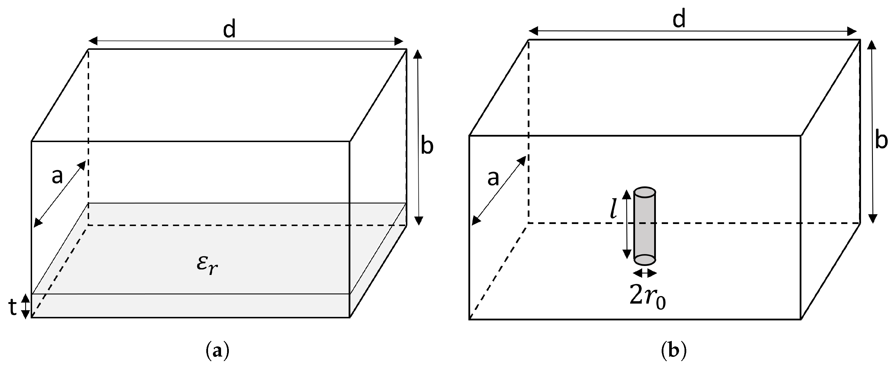
Figure 1. Rectangular cavity perturbed with (a) thin dielectric slab and (b) metallic cylinder in the center.
Instruments 08 00037 g001
Figure 2. (a) Experimental setup with resonant cavity connected to the VNA. (b) IC placed on a plastic platform and holder inside the resonant cavity.
Instruments 08 00037 g002
Figure 3. Authentic ICs (top row). Counterfeit ICs (bottom row).
Instruments 08 00037 g003
Figure 4. Error plot of return loss and resonant frequency values with a 99% CI ( n = 5 ) at the (a) TE101 mode and (b) TE102 mode for the various IC samples.
Instruments 08 00037 g004
Figure 5. Error plot of return loss and resonant frequency values with a 99% CI ( n = 5 ) at the (a) TE103 mode, (b) TE104 mode, and (c) TE201 mode for the various IC samples. (d) Three-component PCA for the various IC samples using return loss and frequency values from the TE103, TE104, and TE201 modes.
Instruments 08 00037 g005
Table 1. Description of ICs used in the evaluation.
Part NumberManufacturerFunction
INA122PTexas InstrumentsInstrumentation amplifier
LM2903PTexas InstrumentsComparator
LT1028CN8Linear TechnologyOperational amplifier
NE555PTexas InstrumentsPrecision timer
SN65176BPTexas InstrumentsDifferential bus transceiver
Disclaimer/Publisher’s Note: The statements, opinions and data contained in all publications are solely those of the individual author(s) and contributor(s) and not of MDPI and/or the editor(s). MDPI and/or the editor(s) disclaim responsibility for any injury to people or property resulting from any ideas, methods, instructions or products referred to in the content.