Abstract
I have proposed a bottom-up technology utilising irradiation with active beams, such as electrons and ions, to achieve nanostructures with a size of 3–40 nm. This can be used as a nanotechnology that provides the desired structures, materials, and phases at desired positions. Electron beam irradiation of metastable θ-Al2O3, more than 1019 e/cm2s in a transmission electron microscope (TEM), enables the production of oxide-free Al nanoparticles, which can be manipulated to undergo migration, bonding, rotation, revolution, and embedding. The manipulations are facilitated by momentum transfer from electrons to nanoparticles, which takes advantage of the spiral trajectory of the electron beam in the magnetic field of the TEM pole piece. Furthermore, onion-like fullerenes and intercalated structures on amorphous carbon films are induced through catalytic reactions. δ-, θ-Al2O3 ball/wire hybrid nanostructures were obtained in a short time using an electron irradiation flashing mode that switches between 1019 and 1022 e/cm2s. Various α-Al2O3 nanostructures, such as encapsulated nanoballs or nanorods, are also produced. In addition, the preparation or control of Pt, W, and Cu nanoparticles can be achieved by electron beam irradiation with a higher intensity.
1. Introduction
The size range of several tens of nanometres represents a transition region from “top-down” to “bottom-up” processes in nanotechnology. The author has proposed a bottom-up technology utilising active beam irradiation to achieve nanostructures with a size of 3–40 nm. Recent developments in focusing and scanning technologies for active beams, such as electrons or ions, in tabletop apparatuses enable the evolution and control of various types of nanostructures, which can provide desirable hybrid structures, materials, and phases at the desired positions on the nanometre scale.
The source of the electron beam used by the author’s group is a transmission electron microscope (TEM) equipped with either an LaB6 filament or a field emission gun. Although TEM has been widely used as an analysis tool for studying nanostructure and element distributions, we consider a specimen stage of 3 mm in diameter as a reaction field, and focused electrons with an intensity more than 50 times higher than that used under normal observation conditions. The electron irradiation intensity ranged from 5×10¹⁹ to 4 × 10²³ e/cm2s (8 × 10⁴–6 × 10⁸ A/m2) in our experiment, and we succeeded in producing oxide-free nanoparticles via electron irradiation of the oxide and facilitated their subsequent manipulation.
In this paper, three topics on the manipulation and control of ceramics and metals by electron beam irradiation are discussed: (1) the preparation of Al nanoparticles and their nanostructure evolution starting from metastable Al2O3, (2) their manipulation by electrons, and (3) the effects of electron irradiation on other nanoparticles, such as Cu, Pt, and W, to prepare nanofilms. This review is based on papers published between 1995 and 2005.
2. Electron Excited Reaction Field
2.1. Overview
In the “Exploratory Research for Advanced Technology” (ERATO) “Tanaka Solid Junction Project,” JST [1], held in 1993–1998, I commenced an innovative challenge to fabricate nano-/microstructures by irradiation with an energy beam such as electrons and ions, based on the proposed concept of an “excited reaction field.” One of the characteristics of such field is that the beams are obtained on the specimen stage of a TEM for electrons, and on the milling/thinning stage for ions. In other words, observation or specimen preparation apparatuses are utilised for their beam source and excited reaction fields. Irradiation with these energy beams has the following merits: first, it facilitates the selection of the site/energy/reaction. Second, it can induce nonequilibrium/catalytic reactions, making it possible to manipulate atomic clusters, synthesise nanomaterials, control the nanostructure and phase, and modify the nanospace.
2.2. Effects of Electron Beam Irradiation on θ-Al2O3
The normal electron beam intensity for observation by a TEM equipped with an LaB6 filament is on the order of 1018 e/cm2s (1600 A/m2) for bright-field imaging and 5 × 10¹⁶ e/cm2s s (80 A/m2) for selected area diffraction measured by a fluorescent plate. We increased the electron beam density by increasing the current in the condenser lens to between 1019 and 1022 e/cm2s to enable electron irradiation of the nanomaterials.
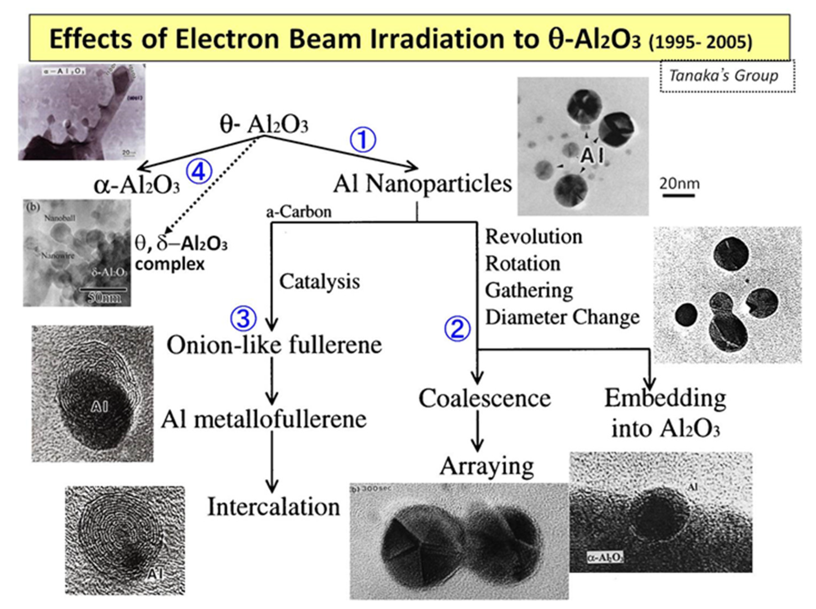
When an electron beam irradiates metastable θ-Al2O3 particles at an intensity of 1020 e/cm2s in a TEM, successive reactions occur: ① Al nanoparticle inducement, ② rotation, revolution, and migration to coalesce/embed, and ③ formation of onion-like fullerenes and Al intercalation, as shown in Figure 1. Furthermore, ④ θ- or δ-Al2O3 nanostructures are obtained under flashing-mode irradiation (rapid switching between 1019 and 1022 e/cm2s).
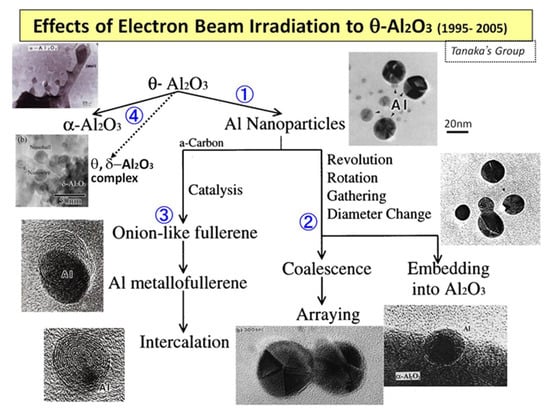
Figure 1.
Evolution of the reactions and nanostructures induced by electron beam irradiation of metastable θ-Al2O3 in TEM. Numbers ①–④ denote the reaction routes explained [1].
3. Nanostructure Evolution
3.1. Al Nanoparticles
The starting material consists mainly of a metastable θ-Al2O3 monoclinic structure accompanied by orthorhombic δ-Al2O3 (Al2O3 allotrope), and it is different from stable α-Al2O3 with a trigonal structure. The θ-Al2O3 powder was synthesised using the vaporised metal combustion method (Admatechs Company Limited) [2].
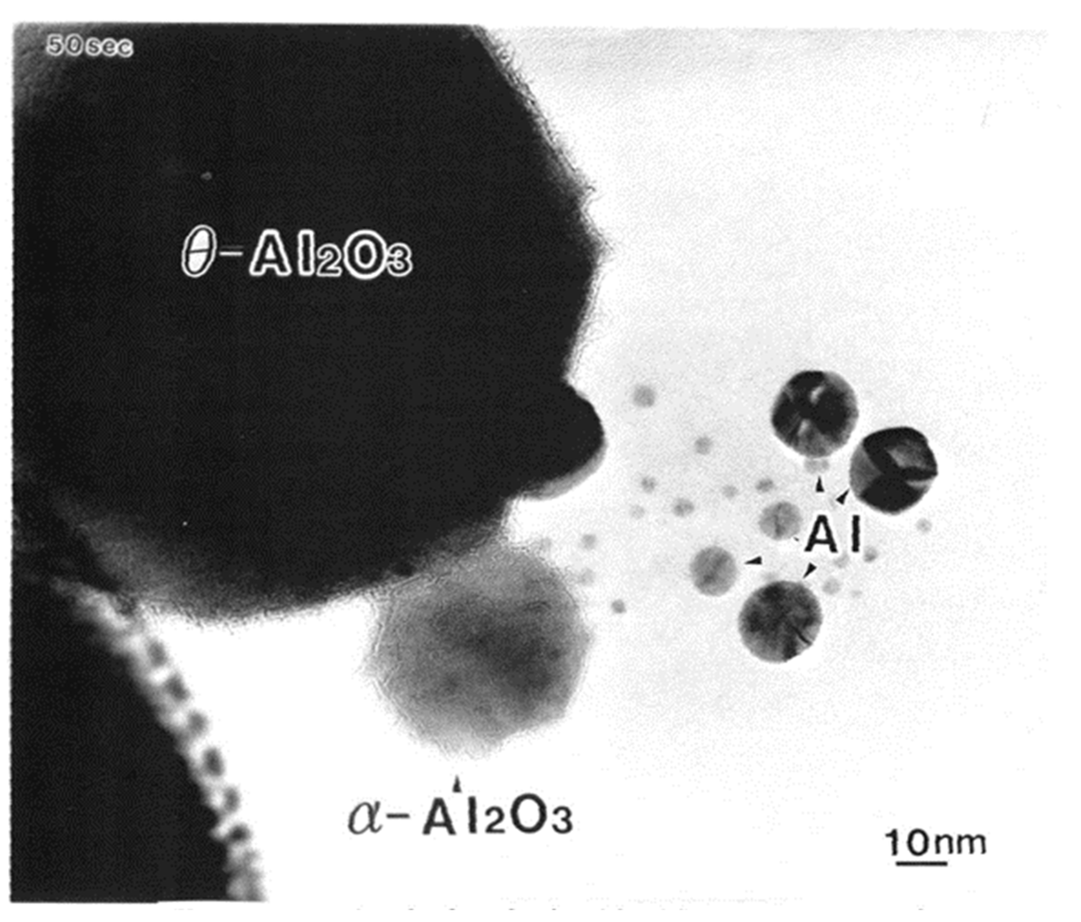
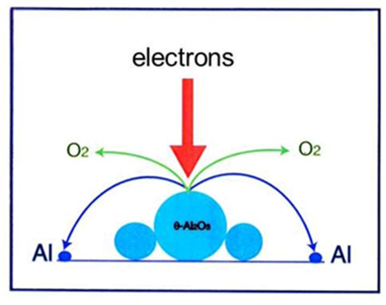
Electron irradiation (2.1 × 10²⁰ e/cm2s for 50 s) of one θ-Al2O3 particle with a diameter of 100 nm on the φ3 mm specimen stage of the TEM led to the formation of Al nanoparticles with a diameter of 2–20 nm and a stable α-Al2O3 particle, as shown in Figure 2 [3]. The TEM used was a JEOL JEM-2010 equipped with an LaB6 filament and a specimen chamber under a vacuum of 10−7 Pa, obtained by a direct coupling sputter ion pump. Under these conditions, the electrons cut the Al-O bond in θ-Al2O3, which was followed by the loss of oxygen to the vacuum and Al atom recombination to form nanoparticles, as schematically shown in Figure 3. In the electron-irradiated area, transformation or rearrangement from θ-Al2O3 to stable α-Al2O3 also occurred.

Figure 2.
Al nanodecahedra of 10–17 nm in diameter and α-Al2O3 nanoparticles obtained by electron irradiation of metastable θ-Al2O3 with an intensity of 2.1 × 10²⁰ e/cm2s in TEM [3].
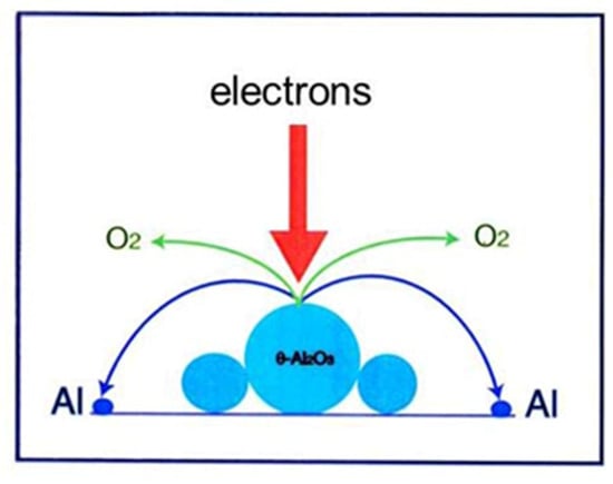
Figure 3.
Schematic of Al nanodecahedra formation by electron irradiation in a TEM. Electrons cut the Al-O bond of metastable θ-Al2O3, which decomposes into Al and O atoms, and finally the Al atoms recombine to form twinned decahedra surrounded by {111} surfaces.
θ- and δ-Al2O3 appear as low-temperature phases in the allotropic transformation from γ-Al2O3 to α-Al2O3 upon heating. The starting powder used in this experiment was obtained by melting Al metal powder, vaporisation, collision of droplets, and quenching into the metastable phase [2]. The powder particles had a spherical shape with an average diameter of approximately 10 µm. No stable α-Al2O3 structure was observed by X-ray diffraction, and an equilibrium thermodynamic consideration was invalid for metastable θ-Al2O3, where the binding energy for Al-O was lower than that for α-Al2O3. The reaction was expected to proceed via a nonequilibrium route. Electron irradiation promoted the decomposition of metastable θ-Al2O3, recombination of Al atoms, loss of a part of oxygen atoms into vacuum, and transformation to stable α-Al2O3, as shown in Figure 3, which resembles one stile of the electron-stimulated desorption.
Al nanoparticles have a twinned decahedron structure surrounded by {111} surfaces, which has been reported in typical face-centred cubic noble metals, such as Au, Pt, or Ag, whereas no report has been published on Al because of its easily oxidised surface. Decahedra appeared with diameters in the range of 10–20 nm, and further electron irradiation of a set of nanodecahedra enabled their manipulation, as discussed in the next section.
3.2. Manipulation
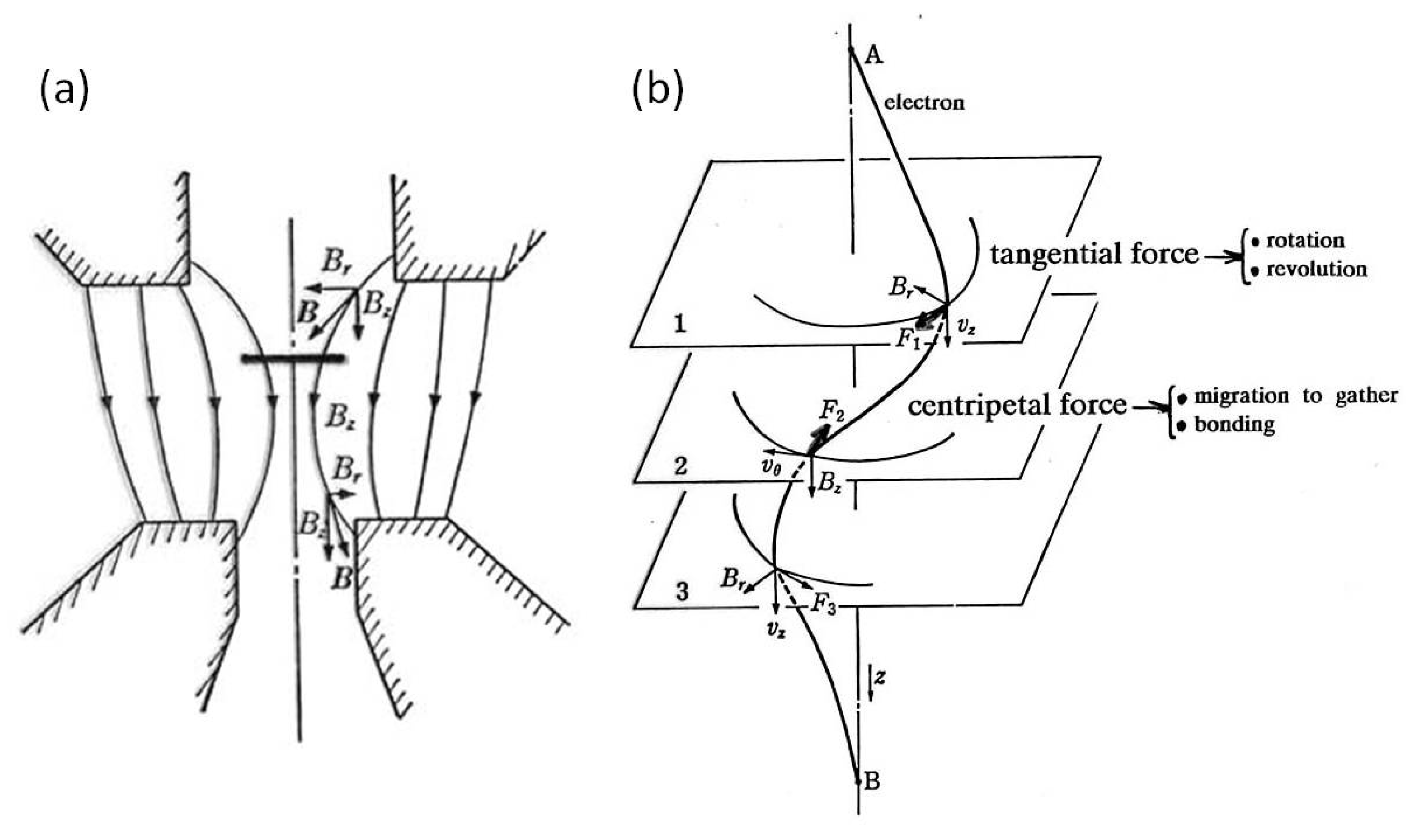
In the ERATO project, TEM has been used not only as an observation apparatus but also as a tool for the manipulation of nanostructures by electrons on the specimen stage. The 200 keV JEM-2010 TEM has a pole piece with a magnetic field of 104 Gauss from top to bottom, where the specimen stage is located slightly above the centre. Based on the kinetic features analysed by Horiuchi et al. [4], the momentum transfer from electrons to nanoparticles is the source of their movement. The spiral trajectory of the electrons causes Al nanoparticles on the specimen stage to experience both a tangential force to rotate and revolve and a centripetal force to migrate, bond, and embed. The features around the specimen stage and the driving forces are illustrated in Figure 4.
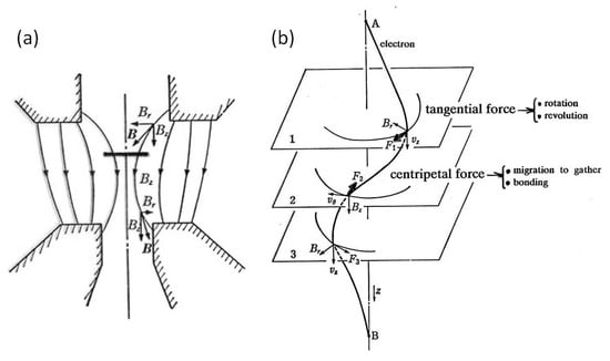
Figure 4.
Model of the interaction between electrons and particles on the specimen stage in TEM. The magnetic field inside a pole piece is 104 Gauss in a 200 keV TEM. (a) Electrons follow a spiral trajectory in the magnetic field to transfer forces or momentum such that (b) the tangential force results in rotation and revolution and the centripetal force induces migration to gather, bond, and embed the particles.
3.2.1. Migration and Bonding
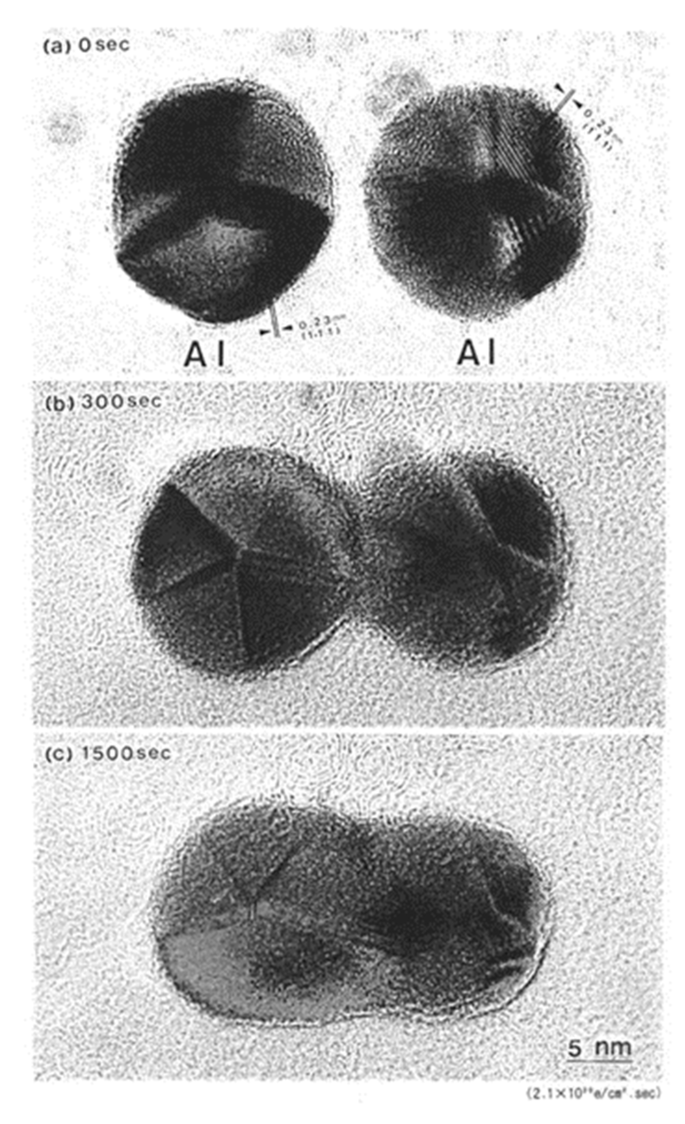
A set of Al nanodecahedra migrated and bonded to the irradiation centre of the electron beam, as shown in Figure 5. Analysis by superposition before and after irradiation, as shown in Figure 5c, revealed that migration, diameter decrease, revolution, and bonding occurred in the course of irradiation over 1200 s at 2.1 × 10²⁰ e/cm2s s, which was mainly due to the centripetal force, as shown in Figure 4. The bonding step of the two nanoparticles is shown in Figure 6, where the (111) planes are aligned parallel by rotation before necking (a) and then necking with Σ3 twinning (b) to eventual coalescence (c) [5,6,7].

Figure 5.
Effects of electron irradiation of a set of Al nanodecahedra inducing migration to the irradiation centre, as well as revolution and rotation. The intensity was 2.1 × 10²⁰ e/cm2s for (a) 0 s and (b) 1200 s. A schematic view of the effect is shown in (c) [6].

Figure 6.
Al nanodecahedra (a) bonded by electron irradiation with an intensity of 2.1 × 10²⁰ e/cm2s after 300 s (b) and coalesced after 1500 s (c). The (111) planes in two Al nanodecahedra were aligned parallel by rotation and exhibited a Σ3 coincidence site lattice (CSL) boundary around the neck at 300 s [5,7].
3.2.2. Rotation and Revolution
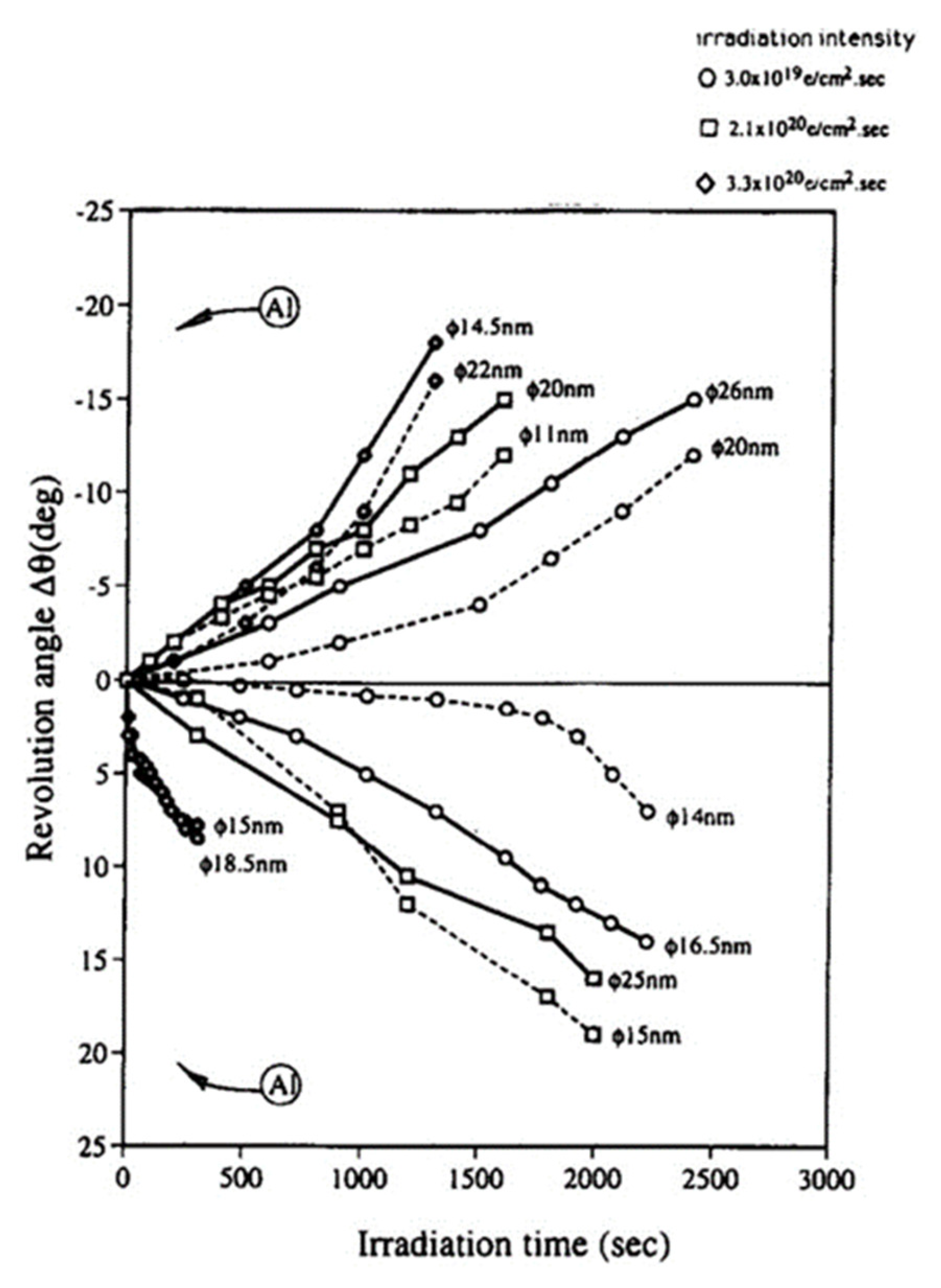
The force acting on the nanoparticle in the magnetic field was also tangential, as well as centripetal, as shown in Figure 4, inducing a clockwise rotation of the nanoparticle on the specimen stage. The speed of rotation measured by the change in angle increased as the irradiation intensity increased for irradiation times less than 1000 s, as shown in Figure 7. The saturation of the rotation with longer exposure is considered to stem from a decrease in the diameter of the particle [6,8].
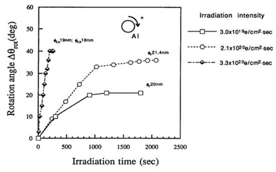
Figure 7.
Rotation of Al nanodecahedra and its dependence on the irradiation intensity ranging from 3.0 × 10¹⁹ to 3.3 × 10²⁰ e/cm2s. The diameter of the nanoparticles is 20 nm, denoted on the line as φ0 [6].
To confirm the effects of the tangential force on the nanoparticle, the magnetic direction in the pole piece was changed from bottom to top by reforming the TEM. Figure 8 shows the revolution behaviour of nanoparticles in both directions of the magnetic field. The clockwise and counterclockwise revolutions of the Al nanoparticles clearly depended on the direction of the magnetic field, and their speed increased as the irradiation intensity increased. The revolution of the nanoparticles was accompanied by their migration, as shown in Figure 5c.

Figure 8.
Clockwise (+) and counterclockwise (−) revolution of Al nanoparticles during electron irradiation controlled by changing the magnetic field direction. The case shown in Figure 5 induced the clockwise revolution, whereas reversal of the magnetic field (bottom to top) induced the opposite direction of revolution. Here, φ indicates the diameter of the initial Al particle [8].
3.2.3. Embedding
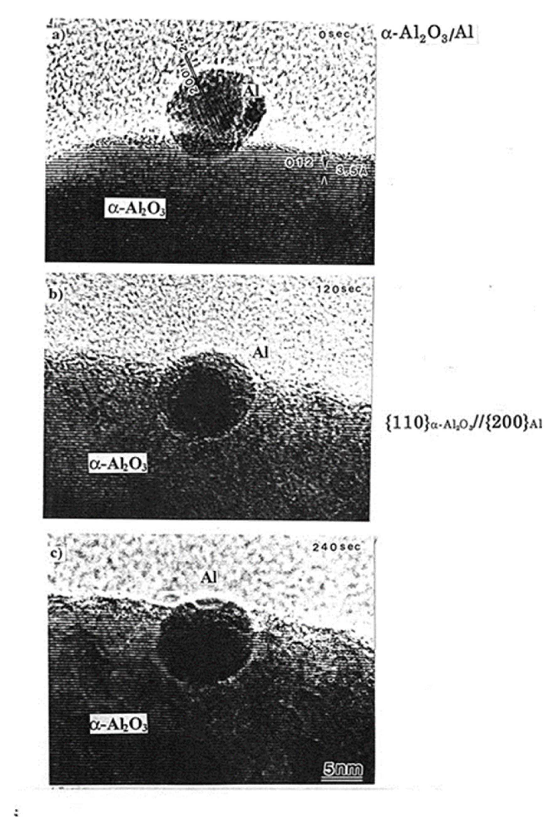
The forces discussed in Section 3.2.1 and 3.2.2 manipulate the nanoparticles to cause migration and embedding into the substrate. Figure 9 shows an example of an Al nanoparticle embedded in the α-Al2O3 matrix following electron irradiation at 1020 e/cm2s, which is attributed to an epitaxial relationship between the two substances. This technique can be utilised for the implantation of catalysts, such as Pt nanoparticles, at the desired position in a matrix [9].
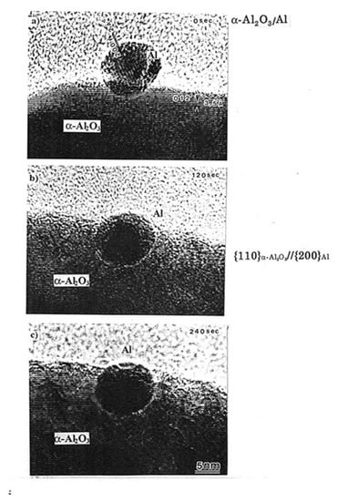
Figure 9.
Al nanoparticle migrated and embedded into the α-Al2O3 matrix by electron irradiation of the order of 1020 e/cm2s for (a) 0 s (b) 120 s and (c) 240 s. The α-Al2O3/Al interface structure exhibits a {11–20}α-Al2O3//{200}Al epitaxial relationship even after electron irradiation for 240 s [9].
3.3. Fullerene and Intercalation
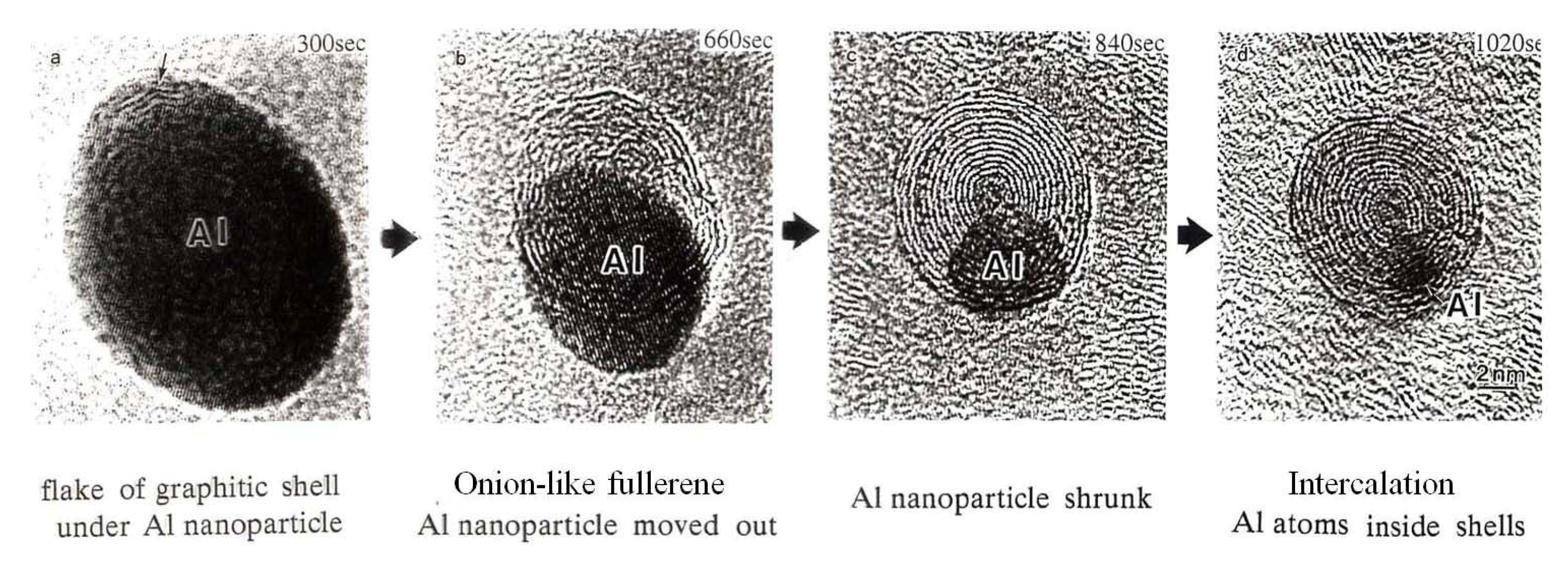
A series of nanostructures were formed on the amorphous carbon nanofilm of the specimen mesh, which was suspended on a Cu grid. Electron irradiation induced the formation of an onion-like fullerene nanostructure under the Al nanoparticles by the catalysis effect and promoted the intercalation of Al atoms between the graphite shells.
3.3.1. Onion-Like Fullerene
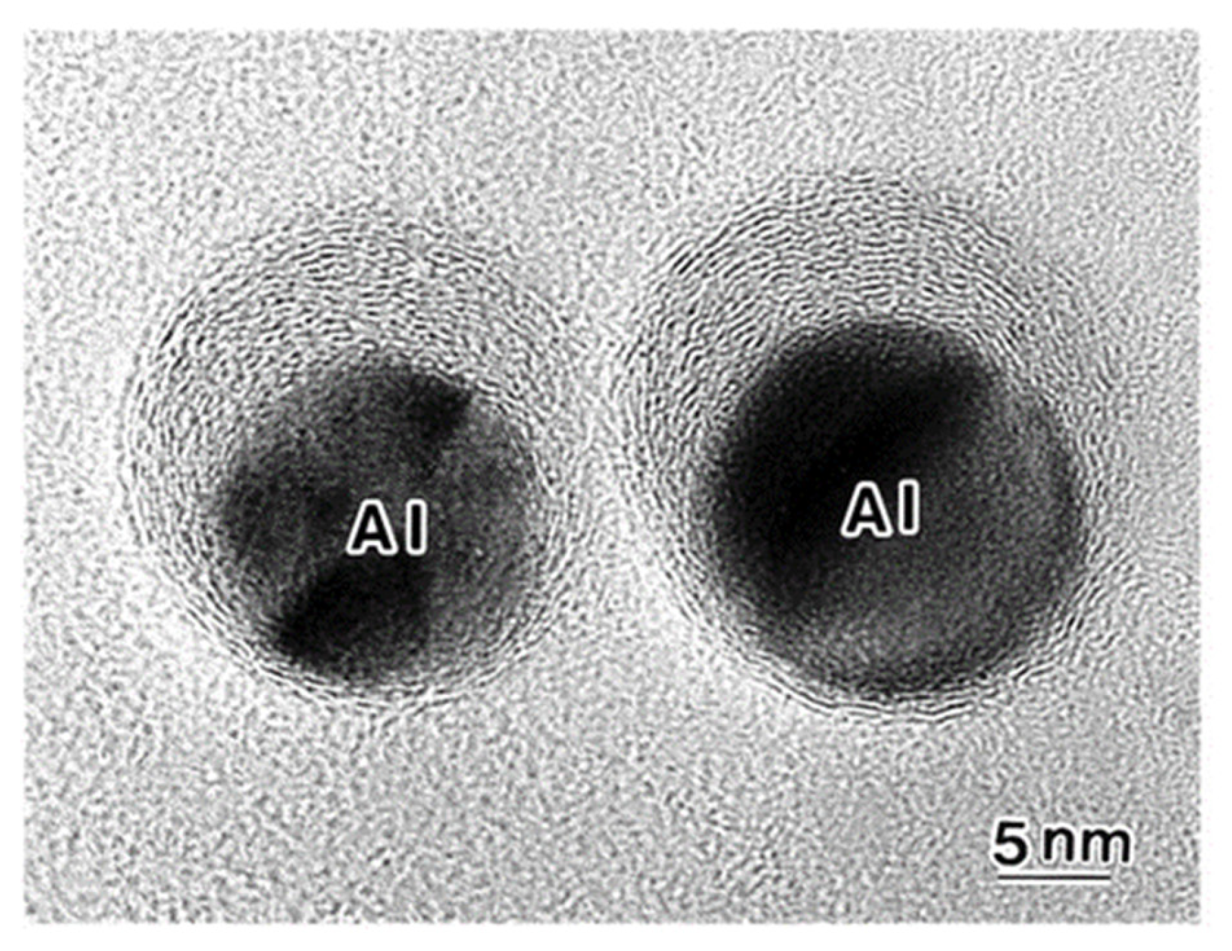
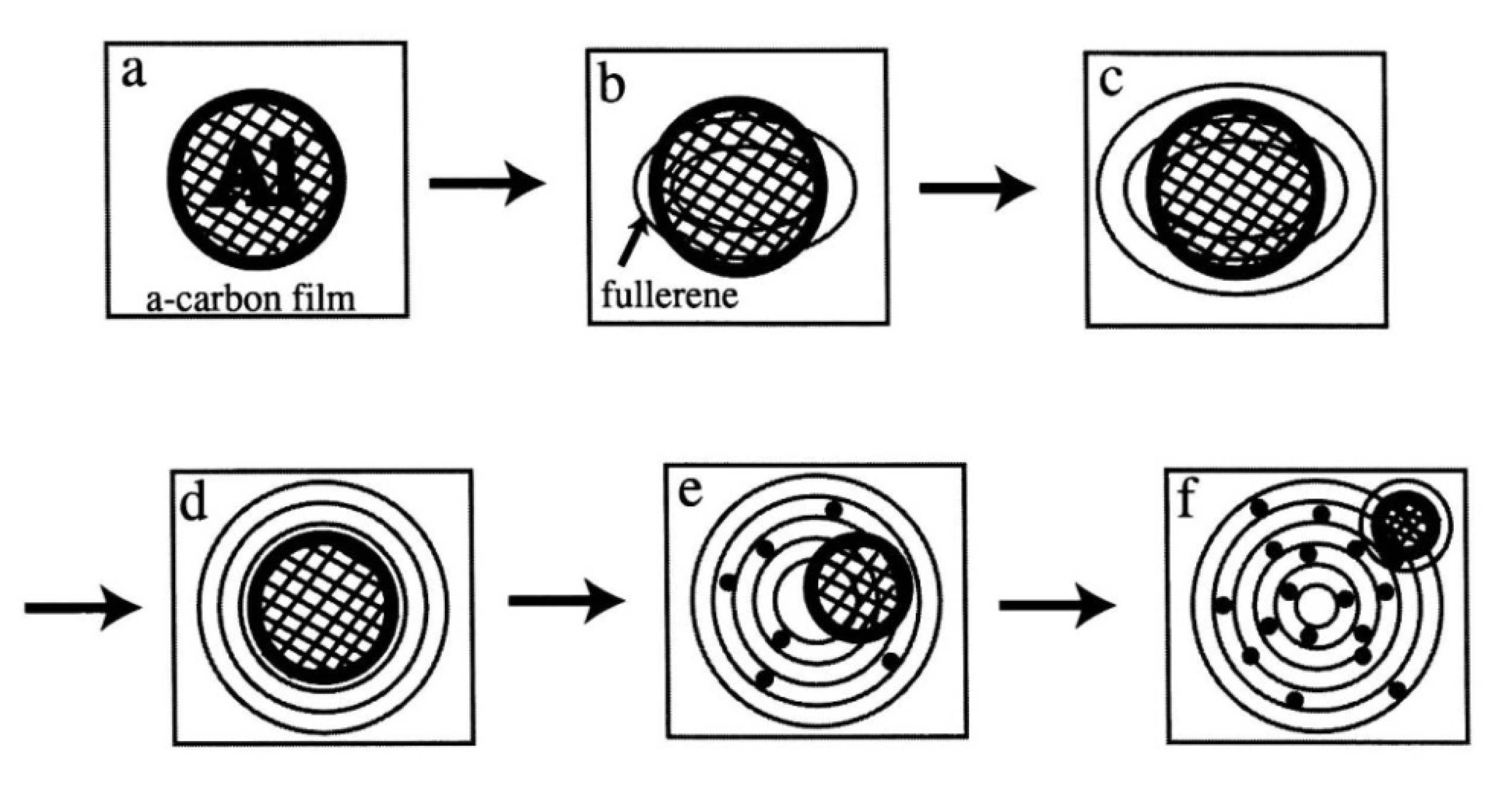
Giant onion-like fullerenes were induced from the amorphous carbon nanofilms under the Al nanodecahedra by electron beam irradiation, as shown in Figure 10. A catalytic reaction nucleated a graphitic flake along the edge of the Al nanoparticle, and prolonged electron irradiation induced the growth of the fullerene, shrinking of the nanoparticles, and intercalation of Al atoms between the shells, as shown in Figure 11 and Figure 12 [5,10].
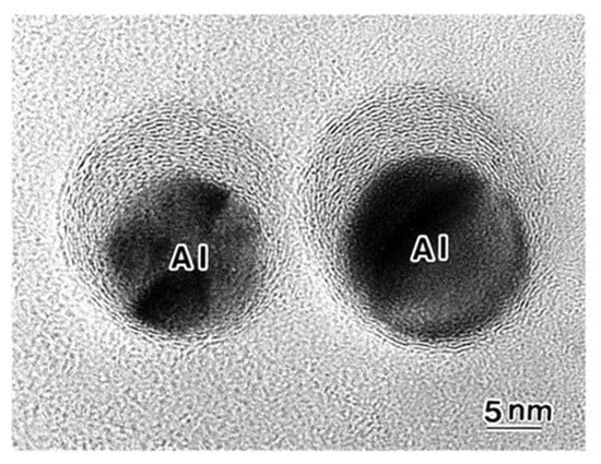
Figure 10.
Giant onion-like fullerenes induced under Al nanoparticles by electron irradiation at an intensity of 3.0 × 10¹⁹ e/cm2s for 2050 s. The Al nanoparticles are surrounded by onion-like fullerene shells [10].
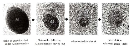
Figure 11.
Series of reactions between Al nanoparticles and the amorphous carbon nanofilm (used as a specimen holder for TEM) induced by electron irradiation with an intensity of 1020 e/cm2s. Reactions proceed from the catalytic formation of (a) a graphitic shell and (b) an onion-like fullerene under the Al nanoparticle, followed by (c) shrinking of the nanoparticle and (d) intercalation of Al atoms inside the shell [10].

Figure 12.
Schematic of a series of interaction behaviours between an Al nanoparticle and an amorphous carbon film under electron irradiation (a:initial). The following steps occurred: a nucleus of the giant onion-like fullerene was first induced under the Al particles (b). Al nanoparticles were encapsulated in the giant onion-like fullerene (c,d). Al nanoparticles moved outside of the giant onion-like fullerene (e), which also induced a new giant onion-like fullerene (f). Finally, intercalation progressed as Al atoms migrated inside the giant onion-like fullerene shells (e,f) [10].
3.3.2. Intercalation
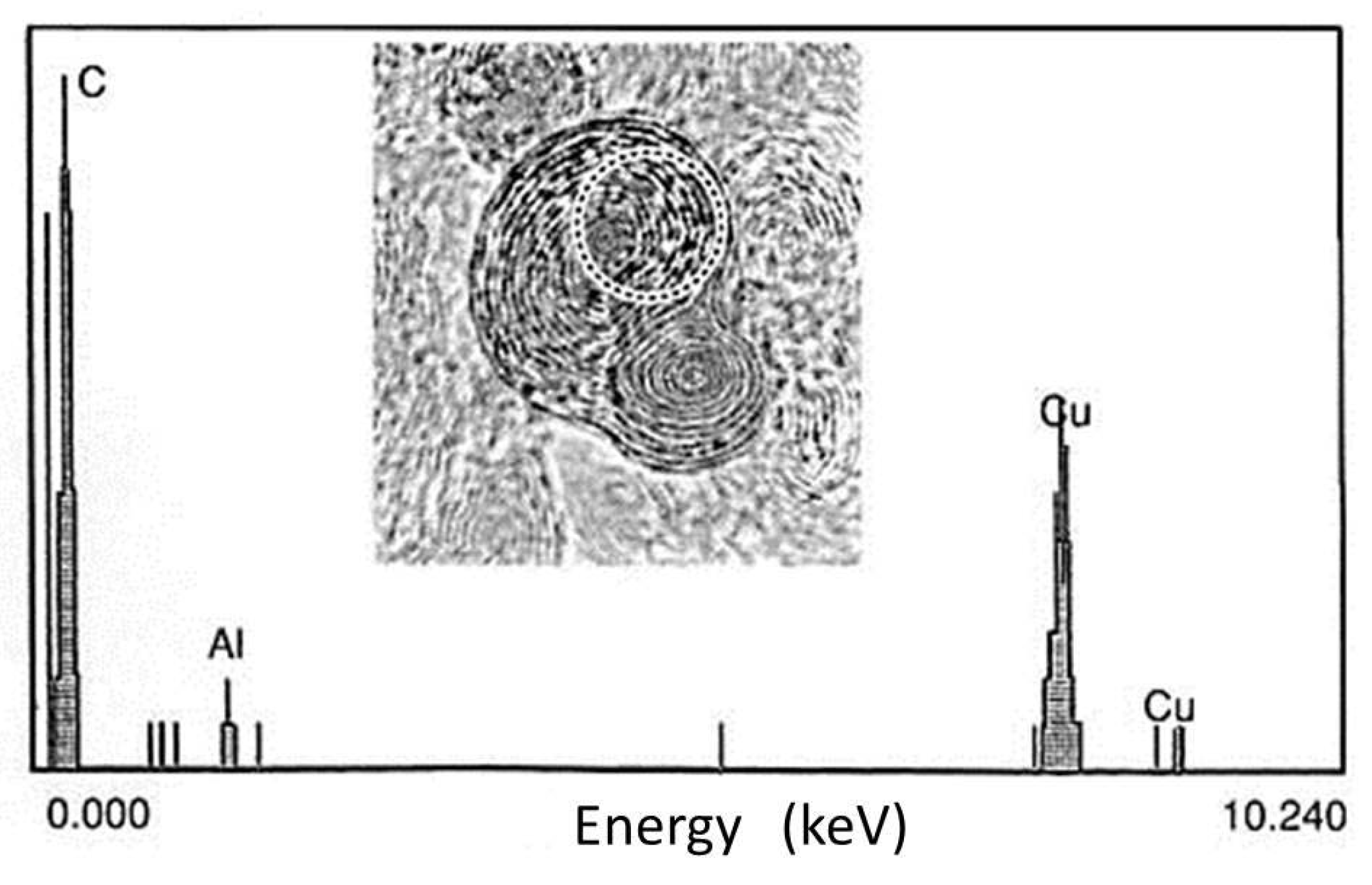
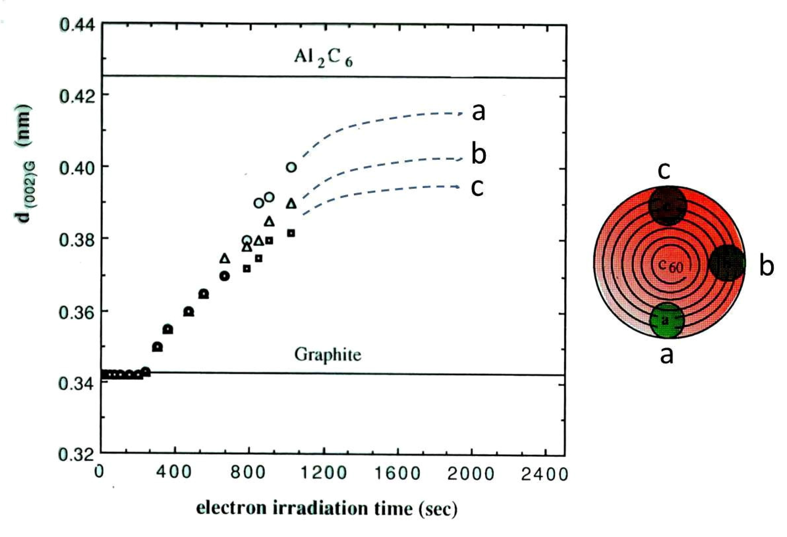
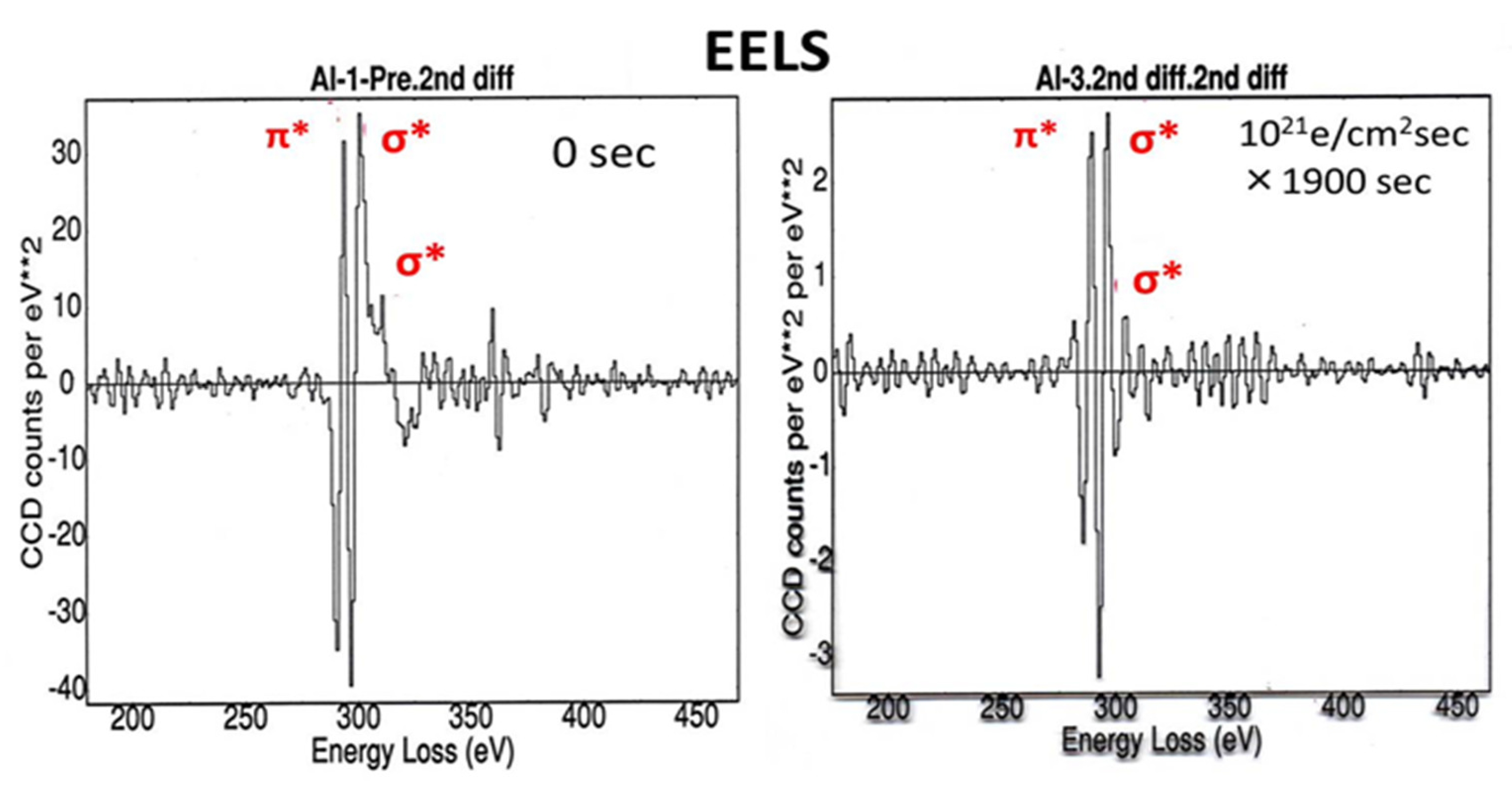
To verify Al atom intercalation into the graphitic shells, an analysis using energy dispersive spectroscopy (EDS), for which the JEM-2010 TEM was equipped, was conducted on the electron irradiated specimen. Figure 13 shows the presence of Al atoms in the circled area of 7 nm in diameter, accompanied by C and Cu in the grid. Moreover, the expansion of the graphite (002) lattice spacing confirmed the presence of Al atoms between the layers, as shown in Figure 14. However, the growth saturated below the composition of Al2C6 owing to the blocking effect of the coexisting Cu atoms or the constraint of passing through multiple carbon layers. Electron energy loss spectra (EELS) also suggested the partial replacement of carbon atoms by Al or Cu atoms through σ bond, sp2, decrease, as shown in Figure 15 [10,11,12].

Figure 13.
EDS analysis of the area inside the dotted circle in the nanostructure shown in Figure 11. The electron probe size was 7 nm in diameter. An Al peak was detected, indicating the possibility of intercalation, whereas the Cu peaks came from the Cu grid of the membrane [10].

Figure 14.
Expansion of the onion-like graphite lattice spacing d(002)G due to Al intercalation, under electron beam irradiation of 1.0 × 10²⁰ e/cm2s. The spacing increased with electron irradiation time and seemed to saturate at 0.425 nm, which coincides with the spacing of the compound Al2C6. The limit of lattice expansion stems either from the blocking effect due to the coexistence of Cu atoms or is constrained by multiple carbon layers [11].

Figure 15.
Second derivative of the EELS of the intercalated structure formed under electron irradiation of 1.0 × 10²¹ e/cm2s for 1900 s. No change is observed in the π-bond between layers after irradiation, whereas the σ-bond, sp2 in-plane, decreased, which suggests the Al and Cu intercalated atoms partially replaced the carbon atoms [12].
4. Al2O3 Derivatives
Continuous electron irradiation of metastable θ-Al2O3 at 2.1 × 10²⁰ e/cm2s produced Al nanoparticles and stable α-Al2O3 particles, as shown in Figure 2. When the intensity and area of electron irradiation changed abruptly (i.e., flashing of the beam), other-shaped nanosized aluminium oxides were obtained. In this section, I present the oxide derivatives of Al2O3 oxides with different shapes and phases.
4.1. α-Al2O3 Nanorods
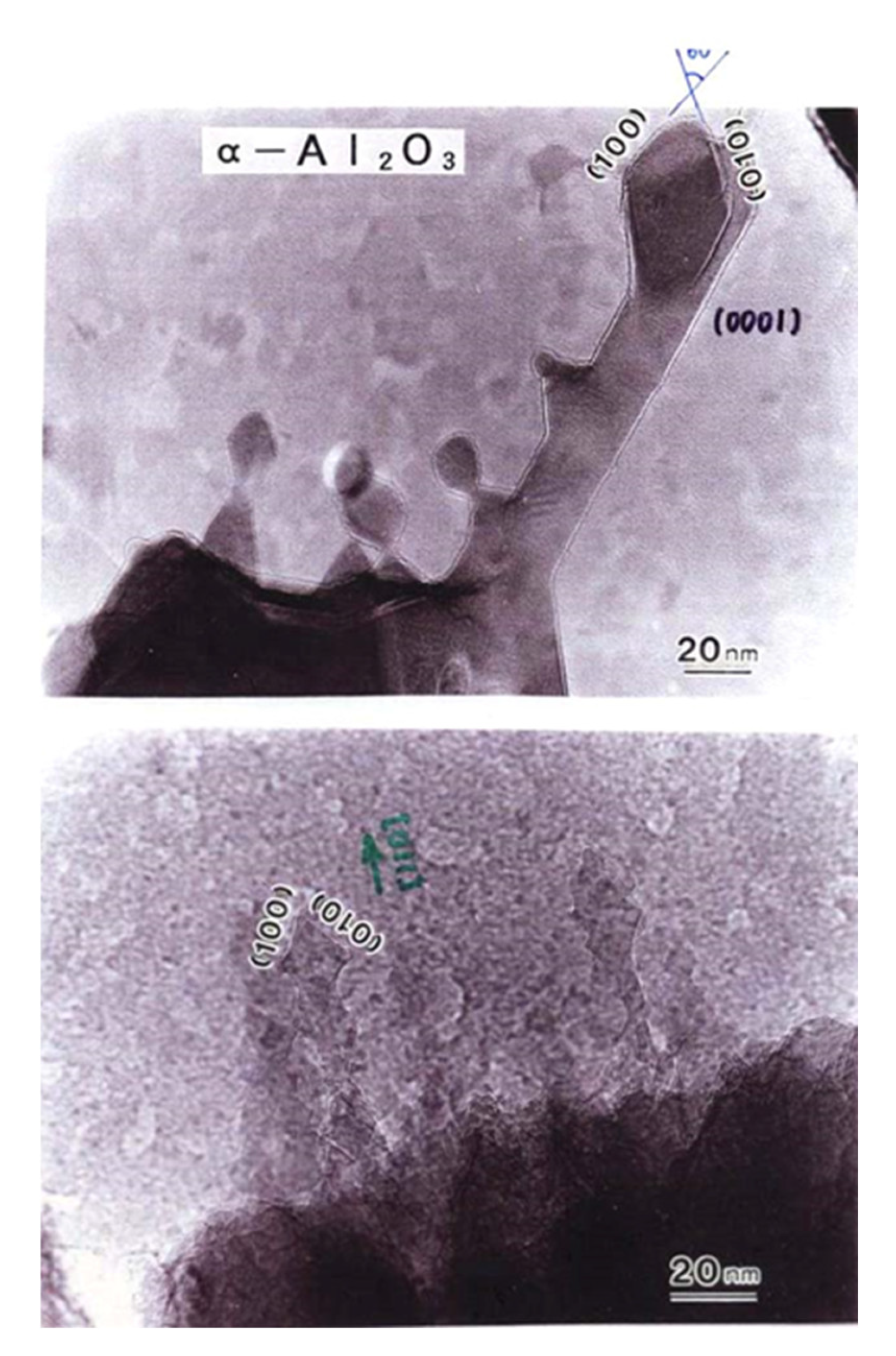
Although α-Al2O3 with a polygonal shape was deposited beside θ-Al2O3 by the recombination of Al and O atoms, the α-Al2O3 nanorods shown in Figure 16 grew from the surface of the parent α-Al2O3. The rods had a faceted structure surrounded by {100} surfaces and grew in the {110} direction. Figure 16 was obtained in situ, in which the nanorods grew without an amorphous oxide film.
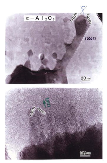
Figure 16.
α-Al2O3 rods epitaxially grown from the θ-Al2O3 surface by electron beam irradiation at 2.1 × 10²⁰ e/cm2s, as shown in Figure 2. The rods grew in the {110} direction and were faceted by {100} surfaces [3].
4.2. δ-, θ-Al2O3 Nanoballs/Nanowires
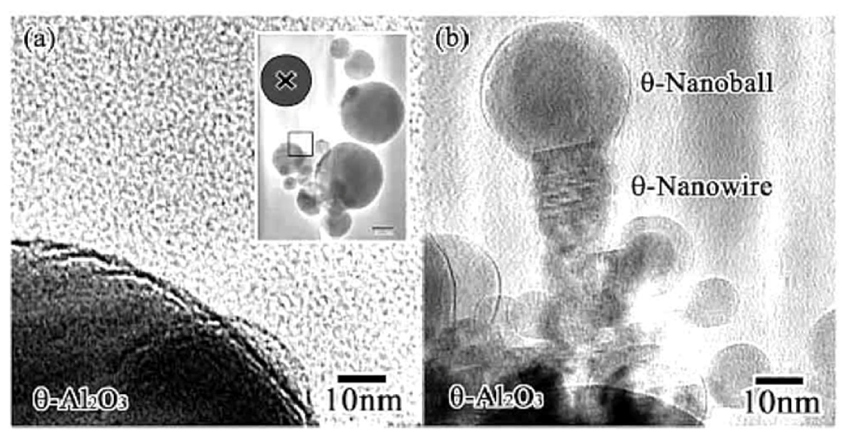
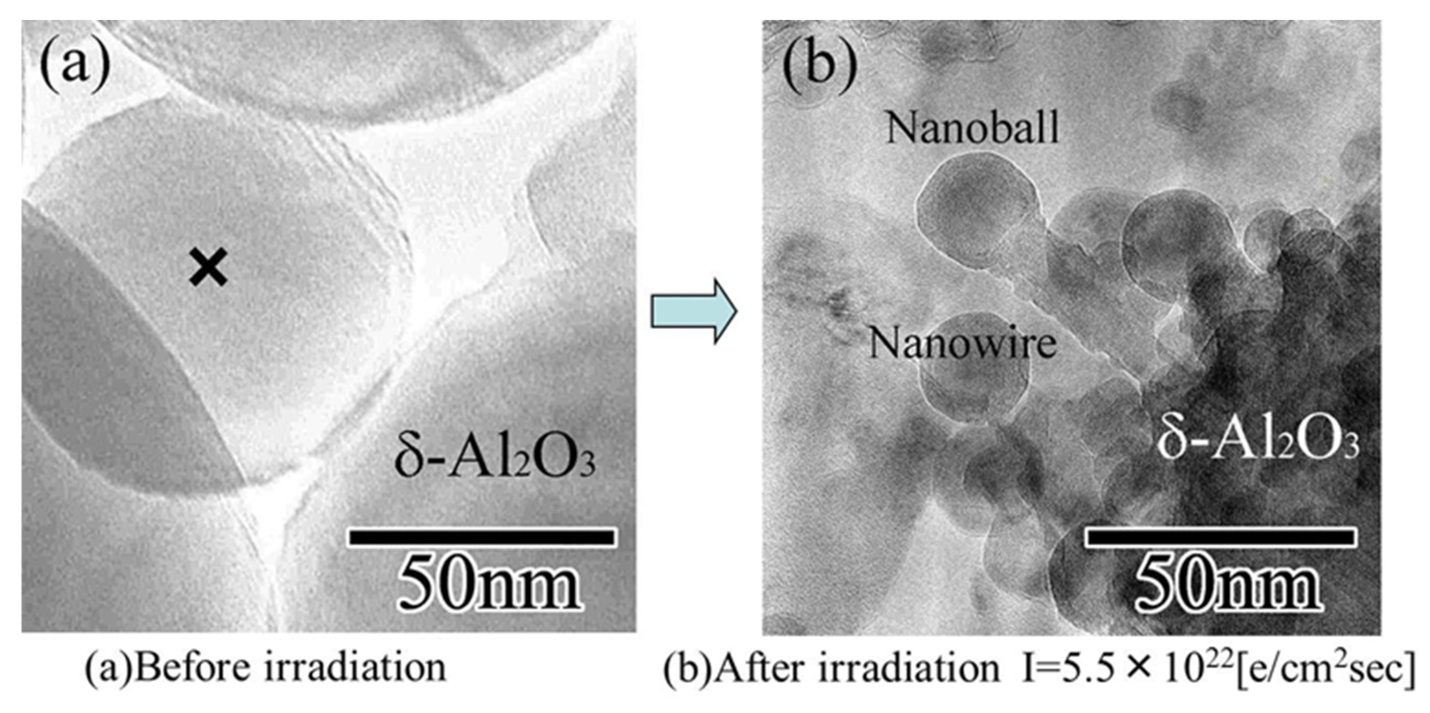
When metastable Al2O3 was irradiated by electrons with a higher density over a short time, the structure was retained, but a different nanostructure was also obtained. Kameyama and Tanaka abruptly switched between intensities of 5.5 × 10²² and 5 × 10¹⁹ e/cm2s in a so-called “flashing mode,” maintaining each state for 0.1 s, which facilitated the formation of θ-, δ-Al2O3 nanorods/nanoballs, as shown in Figure 17, respectively [13].

Figure 17.
θ-Al2O3 nanowire and nanoball grown under flashing mode electron beam irradiation (i.e., rapid switching between intensities of 5.5 × 10²² and 5 × 10¹⁹ e/cm2s). They connected and grew toward the irradiation centre from the original θ-Al2O3 particle surface. The nanowire grew epitaxially maintaining the same plane as the parent θ-Al2O3 particle. (a) θ-Al2O3 particles before irradiation, with X indicating the irradiation centre. (b) θ-Al2O3 nanowire and nanoball grown after electron beam irradiation [13].
Both θ-Al2O3 nanowires and nanoballs grown using flashing-mode electron beam irradiation are shown in Figure 17. They connected and grew toward the irradiation centre from the original θ-Al2O3 particle surface. The nanowire and nanoball had a (111)//(101) epitaxial relationship, as shown in Figure 18. The θ-Al2O3 nanoball was a sphere of 30 nm in diameter covered with an amorphous Al-O layer, suggesting that the impact of a higher irradiance electron beam resulted in a temperature rise of approximately 400 °C, reaction, and rapid cooling without phase transformation. The δ-Al2O3 nanowires and nanoballs shown in Figure 19 were obtained by applying the same flashing electron beam to δ-Al2O3 particles. The diameter of the δ-Al2O3 particles was 20 nm, which was slightly smaller than that of the θ-Al2O3 particles, and no explicit epitaxy relation was observed.

Figure 18.
The interface of the θ-Al2O3 nanowire and nanoball, shown in Figure 17, exhibits a (111)//(101) epitaxial relationship. The nanoball is covered with an amorphous Al-O layer [14].

Figure 19.
δ-Al2O3 nanowire and nanoball grown under flashing mode electron beam irradiation with intensities switching between 5.5 × 10²² and 5 × 10¹⁹ e/cm2s. They connected and grew toward the irradiation centre from the original δ-Al2O3 particle surface. (a) δ-Al2O3 particles before irradiation, with X indicating the irradiation centre. (b) δ-Al2O3 nanowire and nanoball grown after electron beam irradiation [13].
4.3. Al2O3 Nanoparticle Encapsulation
The surface of the Al2O3 particles was easily covered by an amorphous hydrocarbon layer through a reaction with residual gases in the TEM, where CO, H2O, and H2 remained even in a highly evacuated atmosphere. When the particles were irradiated by electrons through the outer layer, their inner volume was pulverised into smaller nanoparticles. An example is shown in Figure 20, for the case in which δ-Al2O3 particles with 200 nm in diameter were transformed into δ- and α-Al2O3 nanoballs with 2–20 nm in diameter, encapsulated by a hydrocarbon skin. This structure was generated by irradiation with an intensity of 1.6 × 10²⁰ e/cm2s, which was as high as that used for nanoparticle preparation and manipulation. Nanoparticle encapsulation technology may be applicable to drug delivery systems in medicine [15].
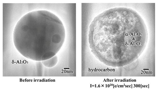
Figure 20.
δ- and α-Al2O3 nanoball-encapsulated structures obtained from δ-Al2O3 particles by electron beam irradiation at 1.6 × 10²⁰ e/cm2s for 300 s. An outer amorphous hydrocarbon layer is formed from residual gas contaminants in TEM [15].
5. Other Nanoparticles
5.1. W Nanoparticles and Manipulation
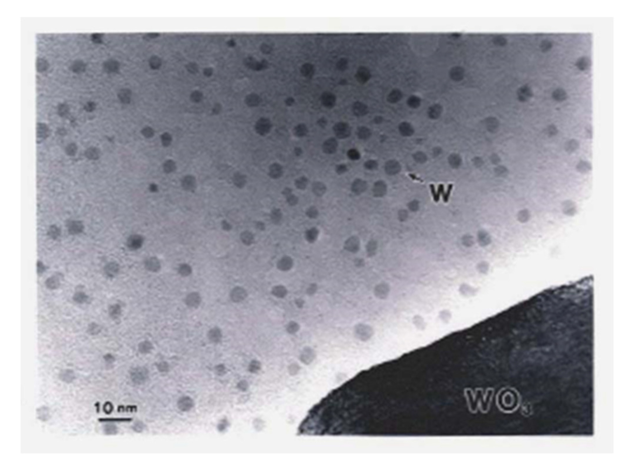
In Section 2, a novel method for preparing oxide-free Al nanoparticles from metastable oxides using electron beam irradiation was discussed. This method can be extended to other nanoparticles of easy oxide-forming elements, such as W. W has a heavier specific weight of 19.3 g/cm3, and W-O has a larger bonding enthalpy such that a higher electron irradiation intensity is required to obtain W nanoparticles from WO3. Although the fundamental electron optics in the TEM were the same as those used for Al nanoparticles, electrons from the field emission source provided a higher intensity of 1023 e/cm2s than the 1020e/cm2s obtained from the LaB6 filament. Using a Hitachi HF-2000 TEM equipped with a field emission gun with an intensity of 4 × 10²³ e/cm2s, Tamou and Tanaka reported the formation of W nanoparticles with an average diameter of 4.3 nm, as shown in Figure 21. The EELS spectra showed no oxygen atoms on the W surface, as shown in Figure 22 [16].
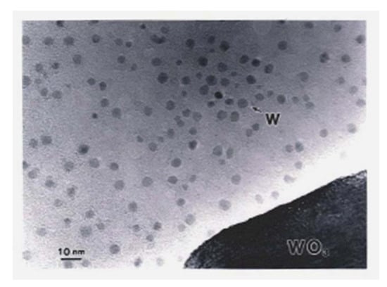
Figure 21.
W nanoparticles deposited by electron beam irradiation of a WO3 particle at 4 × 10²³ e/cm2s (6 × 10⁸ A/m2) for a few seconds. The diameter of the W particles ranged between 2 and 6 nm with an average of 4.3 nm [16].
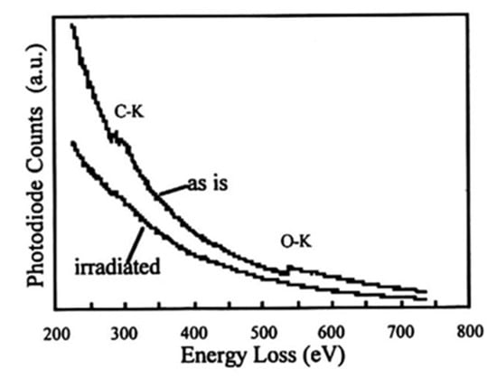
Figure 22.
EELS spectra before and after electron irradiation of WO3. Electron irradiation induced the disappearance of the O-Kα peak to form pure W nanoparticles [16].
5.2. W Migration to Bond and Fullerene Formation
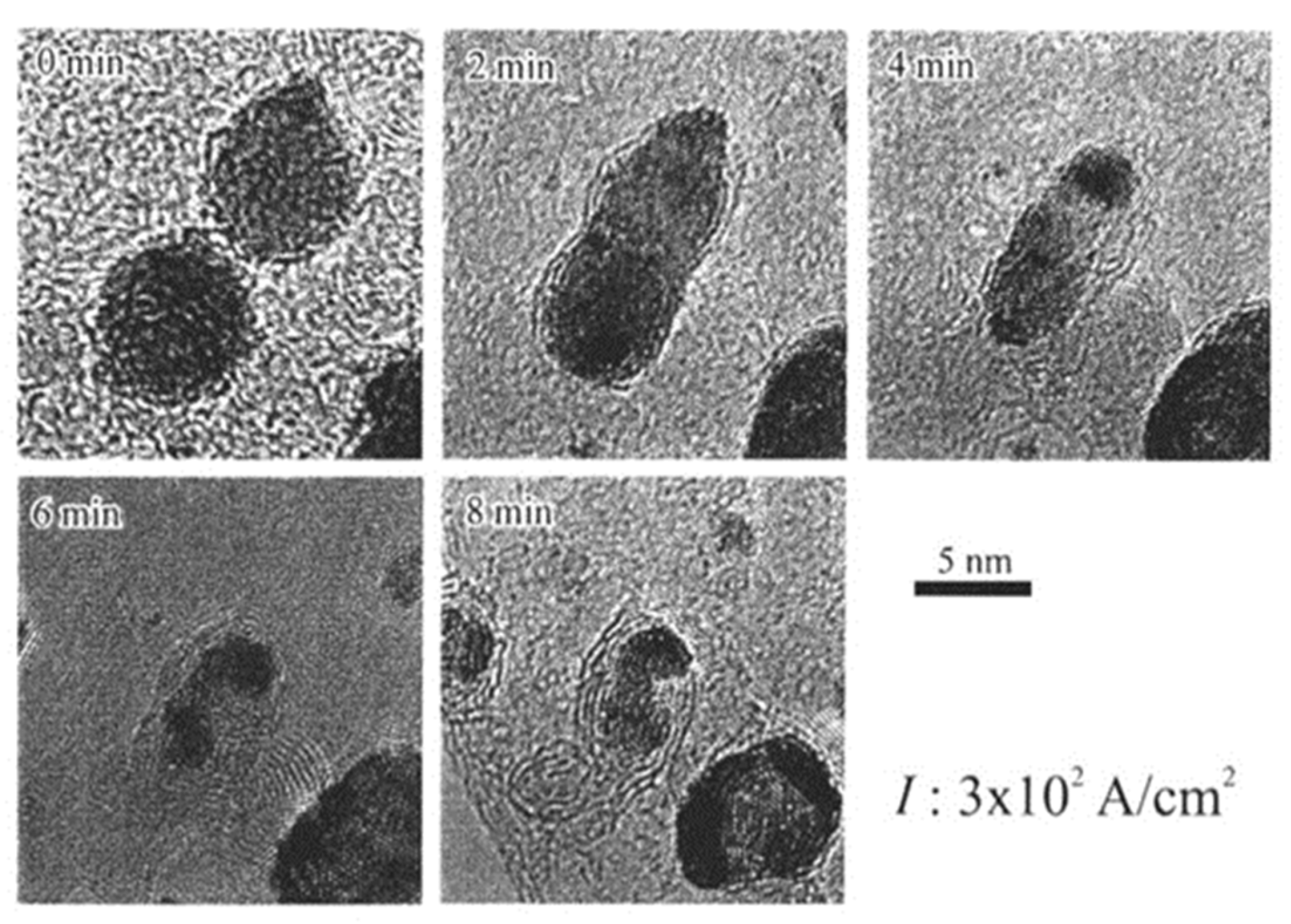
Further electron irradiation of two W nanoparticles, obtained as in Figure 21 at 1.9 × 10²¹ e/cm2s, which is an irradiation 10 times higher than that used to form Al as shown in Figure 6, induced migration, bonding, and coalescence, as shown in Figure 23 [16]. Graphitic shells also nucleated beneath the W nanoparticles from the amorphous carbon film and grew to onion-like fullerene, which is the same phenomenon observed with Al nanoparticles shown in Figure 10, Figure 11 and Figure 12 [16].
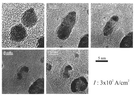
Figure 23.
Effects of electron beam irradiation of W nanoparticles on an amorphous carbon film at 1.9 × 10²¹ e/cm2s (300 A/cm2). W nanoparticles migrated together and coalesced, followed by fullerene formation between the W particles and the carbon film. The general features of nanostructure evolution were the same as those observed with irradiation of Al nanoparticles shown in Figure 10 [16].
5.3. Bonding of Pt and Cu Nanoparticles
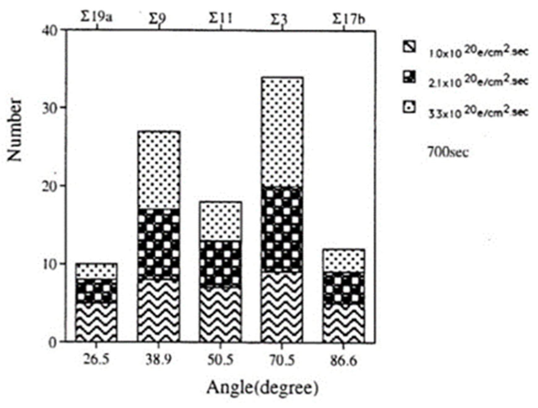
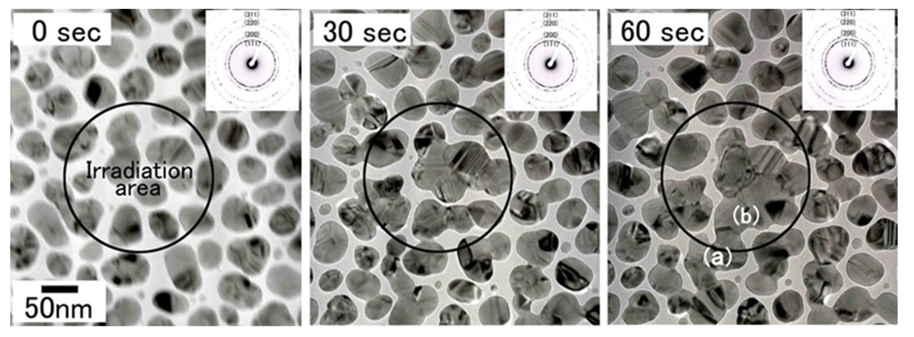
Electron irradiation of a group of Pt and Cu nanoparticles induced bonding to form nanofilms, as shown in Figure 24, Figure 25 and Figure 26. In these cases, nanoparticles were prepared by Ar ion sputtering with a diameter of 10 nm for Pt and 50 nm for Cu. The irradiation intensity for Pt was the same as that for Al, whereas it was 100 times higher for Cu. Bonded Pt/Pt mainly showed three stable Σ3 twin boundaries. The Cu particles migrated to the irradiation centre and bonded, as shown in Figure 26 and Figure 27. The driving force was also the momentum transfer from electrons in the pole piece of the TEM, as shown in Figure 4 and Figure 5 [17,18,19,20].
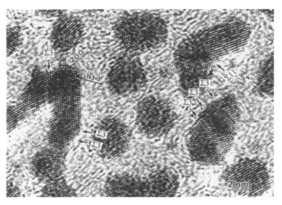
Figure 24.
Pt nanoparticles bonded by electron irradiation with an intensity of 2.1 × 10²⁰ e/cm2s for 700 s. The bonded Pt/Pt nanoparticles had tilt boundaries of Σ3 and Σ11 [19].
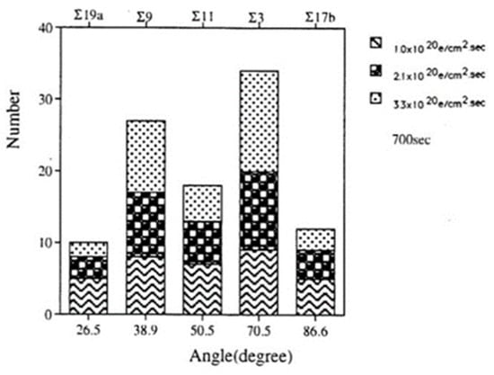
Figure 25.
Histogram of tilt boundaries under electron irradiation at three intensities from 1.0 to 3.3 × 10²⁰ e/cm2s for 700 s. Σ3 CSL boundaries were predominant as a low energy structure [19].
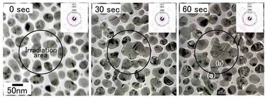
Figure 26.
Change of the bright-field images and electron diffraction patterns of Cu nanoparticles irradiated with electrons at an intensity of 5.5 × 10²² e/cm2s for 60 s. Cu nanoparticles migrated to the irradiation centre and bonded with each other in the marked irradiation area. The electron diffraction patterns, typical Cu Debye rings, did not change during irradiation. The nanostructures of the bonded interface (i.e., CSL) boundary, were obtained in regions (a) and (b) after 60 s of irradiation, as shown in Figure 27 [20].
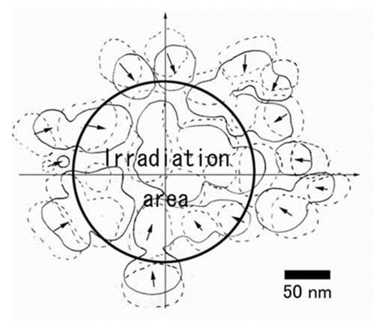
Figure 27.
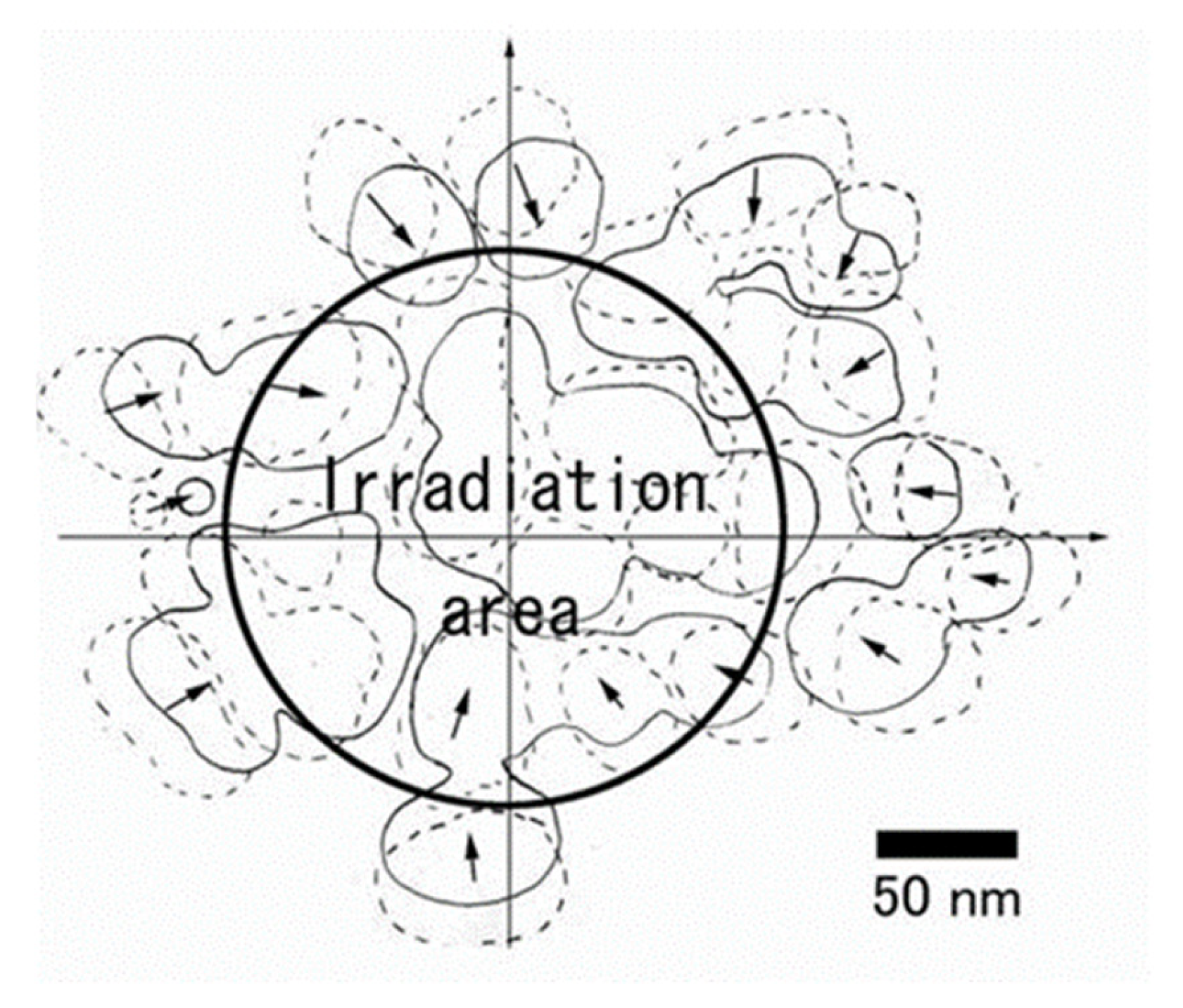
Superposed view of Cu nanoparticle migration and bonding during the irradiation times of 0 s (dotted line) and 30 s (solid line). The circle indicates the electron beam irradiation area of 200 nm diameter. Nanoparticles migrated toward the irradiation centre and finally bonded together. Unbonded small nanoparticles seemed to revolve clockwise around the irradiation centre [20].
6. Nature of Nanoparticle Manipulation and Nanostructure Modification by Electron Beam Irradiation
6.1. Temperature Rise in Al Nanoparticle Manipulation
In Section 3.2, various types of manipulation of Al nanoparticles on the TEM specimen stage were explained. These were migration, bonding, rotation, revolution, and embedding of the nanoparticles, and the driving forces were explained as tangential and centripetal forces, as shown in Figure 4. Another possibility of manipulation is the temperature rise caused by electron irradiation to induce their movement. Xu and Tanaka [10] estimated the temperature rise at the stage as 10° C at most, based on Equation (1) using Fisher’s theory [21]:
where Tm is the maximum temperature of the carbon film, Tg is the temperature of the Cu support grid, namely Tm−Tg is the temperature rise by electron beam irradiation, r is the radius of the irradiation beam, I0 is the intensity of the irradiation beam (1020 e/cm2s), ΔE is the energy loss of the incident electron in the carbon film, when it is <1000 nm thick, a0 is Euler’s constant (0.5772), R is the distance between the irradiation beam centre and the Cu grid bar, k is the thermal conductivity of carbon, and z is the thickness of the carbon film (20 nm).
Tm − Tg = r2I0ΔE[a0 + ln(R/r)2]/4kz,
The heating effect in the localised area under the irradiation condition of 1020 e/cm2s can be a minor effect, and the Lorenz force or the momentum transfer from electrons and ionised atoms is the major effect of the manipulation. This effect is clearly supported by the counterclockwise revolution caused by the magnetic field change, as shown in Figure 8 [8].
6.2. Temperature Rise in Al2O3 Nanocomplex and W Nanoparticles
When θ-Al2O3 was irradiated at a density of 1019–1020 e/cm2s, Al and α-Al2O3 were formed, as shown in Figure 2 and Figure 16, where the reaction proceeded with a small temperature increase of the order of 10 °C, as shown in Section 6.1. On the contrary, the flashing mode of electron irradiation by rapid switching between intensities of 5.5 × 10²² and 5 × 10¹⁹ e/cm2s was applied to θ- and δ-Al2O3 to induce Al2O3 nanoball/nanowire complexes, as shown in Figure 17 and Figure 19 [13]. The higher electron beam intensity increased the temperature by more than 300 °C, as calculated through I0 in Equation (1) by maintaining 5.5 × 10²² e/cm2s even in a short time of less than 0.1 s. This temperature increase was also predicted by Yokota et al. [22]. Rapid and concentrated heat input at the localised resulted in an Al-O recombined nanoball/nanowire complex with epitaxy at the interface, as shown in Figure 18 [14].
Heavy atoms such as W required a higher irradiation intensity of 4 × 10²³ e/cm2s to obtain W nanoparticles, as shown in Figure 21 [16]. Although the binding energy of W–O in the starting material WO3 was smaller than that of Al–O, the W atom is ten times heavier than the Al atom, and required a higher energy for sputtering. A temperature rise was also expected in this irradiation condition, but no melting was observed because of its higher melting point, 3680 K.
6.3. Lorentz Force in Nanoparticle Manipulation
To discuss the mechanism of nanoparticle manipulation in a TEM, the interaction between electrons and nanoparticles on the specimen stage in the magnetic field was analysed. The TEM used in this study was 200 keV JEM-2010, which has a pole piece with a magnetic field of 104 Gauss from top to bottom, where the specimen stage is located slightly above the centre plane. In Figure 4, the electron trajectory is illustrated schematically by Horiuchi et al. [4], and the Lorentz forces F1 and F2 arise from the magnetic components Br and Bz, respectively, with spirally running electrons. The specimen stage is located between planes 1 and 2, and Al, W, Pt, and Cu nanoparticles experience both a tangential force to rotate and revolve and a centripetal force to migrate, bond, and embed. The momentum transfer from electrons to nanoparticles is the source of this movement.
The Lorentz force exerted on one electron, Fe, was roughly estimated by Equation (2)
where me is the mass of one static electron as 9.1094 × 10⁻³¹ kg, ve is the velocity of electrons, considering the relativistic effects at 200 kV as ve = v200 1.3914 = 2.900 × 10⁸ m/s, and r is the distance between the nanoparticle and the irradiation centre. When assuming the experimental case of Al nanoparticles shown in Figure 5, r = 60 nm, the Lorentz force from one electron Fe was 1.277 × 10⁻⁶ N. The total Lorentz force, F, to the Al nanoparticle of 20 nm in diameter with an irradiation time of 1200 s at 1020 e/cm2s was estimated to be 9.63 × 10⁵ N. Although this is the maximum value, which occurs when electrons travel from plane 1 to 2 and the driving force of nanoparticle manipulation changes the direction from tangential to centripetal, it is too high for nanoparticle movement. The author proposes the following reasons: although the electron density was measured on the fluorescent plate beneath the stage, accelerated electron velocity decreased while travelling inside a TEM, and electrons lost their kinetic energy through ionisation of the wall by their impact. The Lorentz force decreased by at least 1/100. The existence of a friction force between nanoparticles and a substrate carbon film could also be one of the causes. The effective cross-section of the nanoparticle might be considered, which decreases the impact of the electrons.
Fe = meve2/r,
The Lorentz force for nanoparticle manipulation is also valid for W, Pt, and Cu, as shown in Figure 23, Figure 24, and Figure 26. Although the time to bond is different depending on the density of the weight, electron irradiation focusing to the localised region will be a candidate technology for fabricating circuits or functional dots by nanoparticle arrays.
7. Summary of the Nanostructure Evolution and Manipulations in the Electron Excited Field
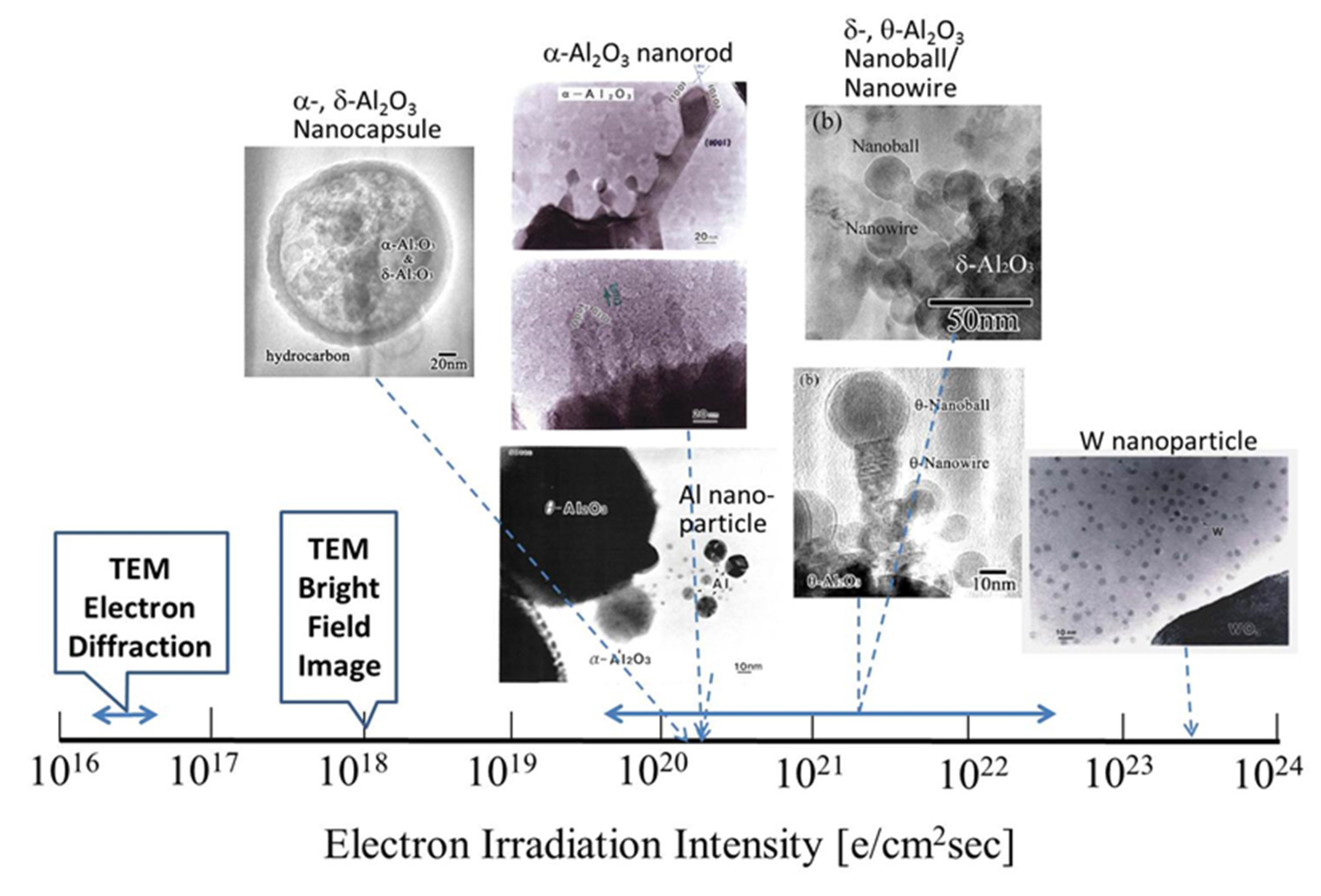
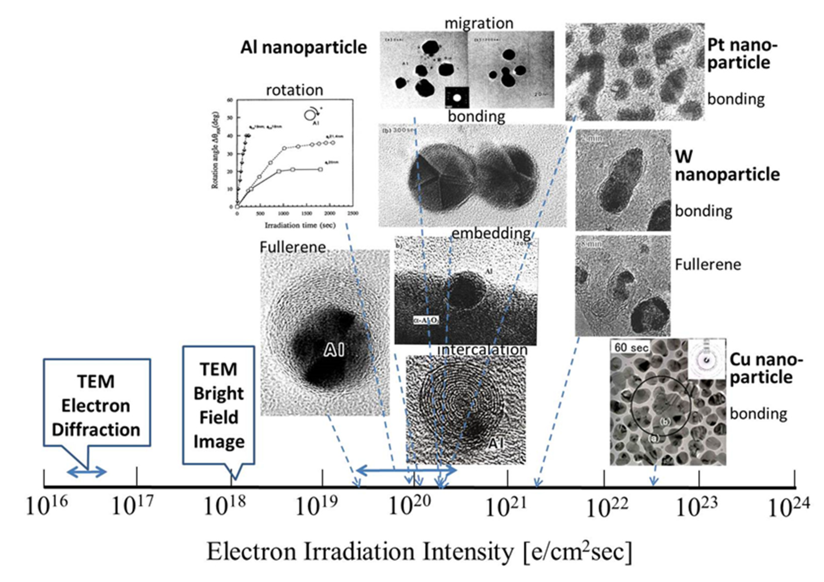
Research conducted by my group on nanostructure evolution by electron beam irradiation from 1995 to 2005 was reviewed. I have utilised electron beams in TEM to synthesise nanomaterials and manipulate their nanostructures, in addition to observing and analysing nanostructures. An overview of the effects of electron irradiation is presented in Figure 28 and Figure 29, where the abscissa is expressed as the electron irradiation intensity on a logarithmic scale. The electron beam was focused for synthesis and manipulation up to 1019–1024 e/cm2s, which is higher than 1016 e/cm2s generally used for electron diffraction and 1018 e/cm2s used for bright-field imaging.
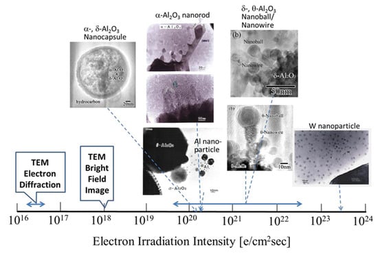
Figure 28.
Nanostructured materials obtained by electron irradiation in TEM. Nanoparticles and nanosized oxides can be induced in an electron excited reaction field. The electron irradiation intensity ranged from 1020–1023 e/cm2s depending on the specific gravity of the materials and the metal-oxygen binding enthalpy of the starting oxide.

Figure 29.
Manipulation of nanomaterials by electron irradiation in a TEM. Nanostructures can be controlled in an electron excited reaction field through migration, bonding, rotation, revolution, embedding, fullerene formation and intercalation. The electron irradiation intensity ranged between 1019–1023 e/cm2s depending on the size and weight of the material.
Figure 28 shows that electron irradiation of metastable θ-Al2O3 provides oxide-free Al nanoparticles, rod-like α-Al2O3, and encapsulated nanoparticles, whereas flashing mode provides θ-, δ-Al2O3 nanoball/nanowire complexes. The formation of W nanoparticles from WO3 requires a higher intensity of more than 1023 e/cm2s. Electrons traveling in a spiral trajectory in the magnetic field of the pole piece transfer momentum to the Al nanoparticles enable various types of manipulation, such as migration, bonding, rotation, revolution, embedding, fullerene formation, and intercalation. The intensity is also more than 100 times higher than that of normal observation conditions, as shown in Figure 29. The combination of such syntheses and manipulation will provide more complicated nanostructures for future applications.
8. Recent Development in Control and Manipulation of Nanostructured Materials
In this review, pioneering works by the author’s group published in 1995–2005 are summarised as a tool for nanomaterial control and manipulation at the TEM room temperature stage. In these works, mediate-accelerating keV was initially used, followed by accompanying magnetic field, and focusing electrons to the localised area. Although there are several works on the effects of electron irradiation, reviews on this topic are scarce. For example, lattice defects such as point defects or stacking faults are introduced as radiation damage in the region of MeV electron irradiation, for which an ultra-high voltage TEM has been used as an experimental simulation. Krasheninnikov et al. published an excellent review paper on the effects of ion and electron irradiation, collecting more than 680 papers [23], which contained derivation and simulation for nanostructured materials. Accompanying magnetic field and focusing electrons to the localised area in TEM are unique technologies for manipulation, which were partly covered in the papers by Zheng et al. [24] and Andres et al. [25]. Zheng et al. reported that the trapping force for one nanoparticle was on the order of 10−9 N in the electron density gradient of 1018−19 e/cm2s [24] which is the same order of magnitude as discussed in Section 6.3. Simulation by first-principle theory using the density of state is important for predicting the formation, growth, and coalescence of nanoparticles [25].
9. Conclusions
The author’s group succeeded in inducing the formation of Al nanoparticles by electron irradiation of metastable θ-Al2O3, followed by manipulation of the nanoparticles. A series of phenomena was observed without heating using high-resolution TEM (HRTEM), with an electron beam intensity as low as 1019–20 e/cm2s. The typical morphology of the nanoparticles was that of a nanodecahedron surrounded by (111) surfaces with twins. Electron beam irradiation of a group of Al nanoparticles promoted their rotation, revolution, and migration to the irradiation centre, resulting in bonding and embedding into an α-Al2O3 matrix. The driving force is considered to be the momentum transfer from electrons spiralling across the pole piece of the HRTEM in a strong magnetic field to the Al nanoparticles. When nanoparticles were placed on an amorphous carbon film, onion-like fullerene nucleated and grew beneath them, and finally, a metallofullerene or Al-atom-intercalated structure was formed by electron irradiation.
To develop the manipulation technology for other types of nanoparticles, an electron beam was used to irradiate Cu nanoparticles of 10–50 nm in diameter at an irradiation intensity of 5.5 × 10²² e/cm2s, Pt nanoparticles at 1.0–3.3 × 10²⁰ e/cm2s, and W nanoparticles derived from WO3 at 9 × 10²⁰ to 4 × 10²³ e/cm2s. The behaviour of Cu, Pt, and W nanoparticles under electron irradiation was similar to that of Al, and a nanofilm was finally formed. The CSL boundary structures at the bonded interface of Cu nanoparticles were found to be unstable Σ7 and Σ13b, which are different from the stable Σ3 obtained in Al and Pt with weaker electron beam irradiation.
The possible scientific contribution of electron irradiation is the synthesis of materials in a metastable state through a nonequilibrium reaction in vacuum, as well as the induction of hybridised nano-/mesostructures. It also enables the study of the nature of materials in a pristine and controlled environment, for example, without the formation of an oxide. From the viewpoint of application to devices, nanosized balls, dots, wires, and tube-forming three-dimensional structured circuits may be used as elements of nanodevices, and chemically active points embedded in the substrate for use as a catalyst can be achieved by the manipulation of electron irradiation. With respect to industrial applications, our technologies will contribute to the development of micro- and nanoelectromechanical systems, memories, photonics, battery electrodes, H2 storage, and more.
Funding
This research partly received funding from ERATO, JST.
Acknowledgments
The author gratefully acknowledges the research scientists at Tanaka Solid Junction Project, JST, BingShe Xu (now: Shaanxi Univ. Sci. Tech.) and Yoshitaka Tamou (now Mitsubishi Materials), and graduate students at Nagoya Institute of Technology, Toru Kameyama (now: Sony GMO Corp.) and Yoshiki Miki (now Nippon Giant Tire Co., Ltd.).
Conflicts of Interest
The author declares no conflict of interest.
References
- TANAKA Solid Junction. Available online: https://www.jst.go.jp/erato/en/research_area/completed/tky_P.html (accessed on 12 July 2021).
- Abe, S.; Ogawa, M.; Kondo, K. Synthesis of Spherical Oxide Particles by Vaporized Metal Combustion Process. In Proceedings of the 4th Silicon for the Chemistry Industry; Norwegian University of Science and Technology: Trondheim, Norway, 1998; Volume 4, pp. 329–338. [Google Scholar]
- Xu, B.S.; Tanaka, S.-I. Phase transformation and bonding of ceramic nanoparticles in a TEM. Nanostruct. Mater. 1995, 6, 727–730. [Google Scholar] [CrossRef]
- Horiuchi, S. High resolution transmission electron microscope. Kyoritsu 1988, 2, 14. [Google Scholar]
- Xu, B.S.; Tanaka, S.-I. Creation and Bonding of Al Nanodecahedron by an Electron Beam. In Proceedings of the Interface 6th Beijing Conference and Exhibition on Instrumental Analysis, Beijing, China, 24–27 October 1995; Volume 111, pp. A31–A32. [Google Scholar]
- Xu, B.S.; Tanaka, S.-I. Control of Nanoscale Interphase Boundaries by an Electron Beam. Mater. Sci. Forum 1996, 207, 137–140. [Google Scholar] [CrossRef]
- Tanaka, S.-I. Control of nanointerfaces by energy beam irradiation. Mater. Sci. Forum 2007, 558–559, 971–974. [Google Scholar]
- Xu, B.S.; Tanaka, S.-I. Behavior and bonding mechanisms of aluminum nanoparticles by electron beam irradiation. Nanostruct. Mater. 1999, 12, 915–918. [Google Scholar] [CrossRef]
- Xu, B.S.; Tanaka, S.-I. Embedding of Al nanoparticle in Al2O3 matrix by electron beam. Supramol. Sci. 1998, 5, 227–228. [Google Scholar] [CrossRef]
- Xu, B.S.; Tanaka, S.-I. Formation of giant onion-like fullerenes under Al nanoparticles by electron irradiation. Acta Mater. 1998, 46, 5249–5257. [Google Scholar] [CrossRef]
- Xu, B.S.; Tanaka, S.-I. Formation of a new electric material: Fullerene/metal polycrystalline film. MRS Proc. 1997, 472, 179–184. [Google Scholar] [CrossRef]
- Tanaka, S.-I. Graphite Intercalation Formed by Electron Irradiation Having KeV Energy. In Symposium of Spring Meeting; The Japan Institute of Metals and Materials: Tokyo, Japan, 2019; p. 3. [Google Scholar]
- Kameyama, T.; Tanaka, S.-I. Alumina nanostructures formed by electron beam irradiation. J. Ceram. Soc. Jpn. 2004, 112-1, S930–S932. [Google Scholar]
- Kameyama, T.; Tanaka, S.-I. Nanostructure Derivation by Electron Beam Irradiation. In Proceedings of the International Conference on Novel Materials Processing by Advanced Electromagnetic Energy Sources (MAPEES’04), Osaka, Japan, 19–22 March 2004. [Google Scholar]
- Kameyama, T. Control of Ceramic Nanostructures by Electron Beam Irradiation. Master’s Thesis, Nagoya Institute of Technology, Nagoya, Japan, March 2004. (In Japanese). [Google Scholar]
- Tamou, Y.; Tanaka, S.-I. Formation and coalescence of tungsten nanoparticles under electron beam irradiation. Nanostruct. Mater. 1999, 12, 123–126. [Google Scholar] [CrossRef]
- Xu, B.S.; Tanaka, S.-I. Pt cluster bonding and fullerene formation in HRTEM. In Proceedings of the International 6th Beijing Conference and Exhibition on Instrumental Analysis, Beijing, China, 24–27 October 1995; pp. A33–A34. [Google Scholar]
- Xu, B.S.; Iwamoto, C.; Tanaka, S.-I. Bonding Behavior of Platinum Nanoparticles under Electron Beam Irradiation in a High Resolution Transmission Electron Microscope. In Proceedings of the Interface Science and Materials Interconnection JIMIS-8, Toyama, Japan, 1–4 July 1996; pp. 395–398. [Google Scholar]
- Xu, B.S.; Tanaka, S.-I. Formation and bonding of platinum nanoparticles controlled by high energy beam irradiation. Scr. Mater. 2001, 44, 2051–2054. [Google Scholar] [CrossRef]
- Miki, Y.; Tanaka, S.-I. Migration and Bonding of Cu Nanoparticles Induced by Electron Beam Irradiation. In Proceedings of the International Conference on New Frontiers of Process Science and Engineering in Advanced Materials, Kyoto, Japan, 24–26 November 2004; pp. 52–57. [Google Scholar]
- Fisher, S.B. On the temperature rise in electron irradiated foils. Radiat. Effects 1970, 5, 239–243. [Google Scholar] [CrossRef]
- Yokota, T.; Murayama, M.; Howe, J.M. In situ transmission-electron-microscopy investigation of melting in submicron Al-Si alloy particles under electron-beam irradiation. Phys. Rev. Lett. 2003, 91, 265504. [Google Scholar] [CrossRef] [PubMed]
- Krasheninnikov, A.V.; Nordlund, K. Ion and electron-induced effects in nanostructured materials. J. Appl. Phys. 2010, 107, 071301. [Google Scholar] [CrossRef]
- Zheng, H.; Mirsaidov, U.M.; Wang, L.-W.; Matsudaira, P. Electron Beam Manipulation of Nanoparticles. Nano Lett. 2012, 12, 5644–5648. [Google Scholar] [CrossRef] [PubMed]
- Andres, J.; Longo, E.; Gouveia, A.F.; Costa, J.P.C.; Gracia, L.; Oliveira, M.C. In-situ formation of metal nanoparticles through electron beam irradiation: Modeling real materials from First-Principles calculations. J. Mater. Sci. Eng. 2018, 7, 1000461. [Google Scholar] [CrossRef]
Publisher’s Note: MDPI stays neutral with regard to jurisdictional claims in published maps and institutional affiliations. |
© 2021 by the author. Licensee MDPI, Basel, Switzerland. This article is an open access article distributed under the terms and conditions of the Creative Commons Attribution (CC BY) license (https://creativecommons.org/licenses/by/4.0/).

