Review

Femtosecond Laser-Based Additive Manufacturing: Current Status and Perspectives

1
Department of Physics, American University of Sharjah, Sharjah 26666, United Arab Emirates
2
Materials Science and Engineering Program, College of Arts and Sciences, American University of Sharjah, Sharjah 26666, United Arab Emirates
3
Department of Mechanical Engineering, Indian Institute of Information Technology, Design and Manufacturing, Kancheepuram, Chennai 600127, India
4
Department of Mechanical Engineering, American University of Sharjah, Sharjah 26666, United Arab Emirates
5
Department of Civil Engineering, American University of Sharjah, Sharjah 26666, United Arab Emirates
*
Author to whom correspondence should be addressed.
Quantum Beam Sci. 2022, 6(1), 5; https://doi.org/10.3390/qubs6010005
Submission received: 9 December 2021 / Revised: 4 January 2022 / Accepted: 7 January 2022 / Published: 18 January 2022
(This article belongs to the Special Issue Laser Assisted Manufacturing)

Abstract

:
The ever-growing interest in additive manufacturing (AM) is evidenced by its extensive utilisation to manufacture a broad spectrum of products across a range of industries such as defence, medical, aerospace, automotive, and electronics. Today, most laser-based AM is carried out by employing continuous-wave (CW) and long-pulsed lasers. The CW and long-pulsed lasers have the downside in that the thermal energy imparted by the laser diffuses around the irradiated spot and often leads to the creation of heat-affected zones (HAZs). Heat-affected zones may degrade the material strength by producing micro-cracks, porous structures and residual stresses. To address these issues, currently, attempts are being made to employ ultrafast laser sources, such as femtosecond (fs) lasers, in AM processes. Femtosecond lasers with pulse durations in the order of 10 15   s limit the destructive laser–material interaction and, thus, minimise the probability of the HAZs. This review summarises the current advancements in the field of femtosecond laser-based AM of metals and alloys. It also reports on the comparison of CW laser, nanosecond (ns)/picosecond (ps) lasers with fs laser-based AM in the context of heat-affected zones, substrate damage, microstructural changes and thermomechanical properties. To shed light on the principal mechanisms ruling the manufacturing processes, numerical predictions are discussed and compared with the experimental results. To the best of the authors’ knowledge, this review is the first of its kind to encompass the current status, challenges and opportunities of employing fs lasers in additive manufacturing.

1. Introduction

Additive manufacturing (AM—commonly referred to as 3D printing) has already revolutionised industry and is positioned to make a notable impact across a wide range of sectors [1,2]. This is primarily induced by the significant simplifications and freedom in the design process combined with the adaptability of 3D printing to an impressively wide range of materials not shared by any other manufacturing technique [3]. Although the potential benefits of 3D printing can be exploited in a wide range of applications and industries, including aerospace [4,5,6,7,8,9], automotive [7,10], defence sectors [11], jewellery making [12], construction [13], electronics [14], food [15], health care [10,16,17], footwear [18], clothing [19], sports [20] and others [21], utilisation in the biomedical is of special interest due to the relatively complex requirements and intricate designs commonly encountered in these fields. The interest in AM continues to grow, and current research and development efforts span across almost all relevant aspects such as the utilised materials, 3D printing technology, post-processing treatments, and optimisation of processing parameters in terms of design and fabrication. One of the major advantages of 3D printing is the ability to adapt and optimise this manufacturing technique to all materials including polymers, ceramics, metals, and composites [1]. Such versatility is not shared by any other manufacturing technique. AM of metals is of particular importance due to the fact of their desirable properties in many applications (e.g., load-carrying capacity). Steel, titanium, aluminium, nickel-based superalloys, iron, copper, gold, and silver have all been successfully processed, even at an industrial scale in some cases [22,23,24]. Such efforts are no longer limited to lab-scale specimens as adoption by industry continues to grow. The aerospace industry was among the first to adopt AM technology for large-scale production. For example, GE aviation employed AM to print nozzles for its LEAP engines. In addition to reducing the total parts count from 20 to 5, durability was also found to be enhanced by a factor of five [25,26]. Similarly, Boeing is saving millions per plane through the use of AM. As of now, more than 70,000 AM parts fly through Boeing programs [27].
Although various techniques have been developed over the years for AM-based synthesis, including material extrusion (ME), direct energy deposition (DED), powder bed fusion (PBF), fused deposition modelling (FDM), sheet lamination (SL) and binder jetting (BJ) [28], the methods that rely on the utilisation of metal powders have been more widely adopted by industry (i.e., PBF, DED and BJ processes). The metal AM systems are usually composed of a powder delivery system and an energy delivery system [29]. In PBF systems, selective laser melting (SLM) or selective laser sintering (SLS) are key processes. In SLM or SLS, the material will heat up and subsequently melt utilising a laser source. At present, metal AM technologies are predominantly reliant on long-pulsed lasers or CW lasers to process materials [30,31]. In general, CW lasers are utilised for fabricating larger parts, whereas pulsed lasers are considered when fabricating precise and thin parts [32]. In the case of CW laser-based AM, there are certain important process parameters that influence the quality of the produced parts using SLM. This includes hatch spacing, scanning speed, laser power and layer thickness [33,34]. In any SLM process, along with these parameters, the light absorptance and the laser energy density play vital roles in melting and sintering. Despite the significant progress made, there are certain challenges that must be overcome such as accuracy and reduced materials usage [35]. In addition, some materials continue to pose challenges and are difficult to process using AM. For example, some ceramics and refractory metals, due to the fact of their high melting temperatures and high thermal conductivity [36], are still difficult to process using CW or long-pulsed laser-based AM technologies. To process such materials, novel technologies and new processes must be developed to reach very high temperatures while causing minimal heat-affected zones (HAZs), along with good precision and accuracy at sub-micron levels. In this regard, ultrafast lasers (i.e., picosecond (ps) and femtosecond (fs) lasers) are well suited for lifting the shortcomings of the existing additive manufacturing techniques, especially in situations where high melting point materials are involved or extreme precision and reproducibility are required [7,37]. Although AM via ultrafast lasers is a relatively new area, recent works have already highlighted its huge potential and advantages over the use of CW lasers [38]. In short, the main advantages of ultrashort pulsed lasers over CW lasers are increased part resolution [39,40], rapid cooling rate, reduced residual stresses, reduced oxidation effect, lower substrate damage compared to CW laser, suitable to process dielectrics and better wettability [41]. These aspects will be discussed in further detail throughout this article.
The use of ultrafast lasers as a manufacturing tool is gaining notable momentum across various industries. In a recent study, the global ultrafast lasers market was predicted to cross USD 1.43 billion by 2020, a number that is further expected to reach the USD 3.31 billion milestone by 2026 with an estimated compound annual growth rate (CAGR) of 16.6% between 2021 and 2026 [42]. Though the initial investment is high for such laser technologies, the significant advantages (e.g., precise manufacturing and reduced HAZs) provide justification for their use in medical, aerospace and military applications. As noted above, fs lasers are being explored for precise material processing due to the ultrashort pulse duration in the range of a few hundred fs that produces lower laser–matter interaction times and reduces HAZs. In addition to pulse duration, the scanning speed and pulse repetition rate are also major deciding factors for precise AM. Fs laser sources produce higher peak intensities compared to CW lasers or long-pulsed lasers. This allows for rapid energy delivery into the material and paves the way to achieve localised heating [43]. Apart from this, fs lasers have high penetration depth in a short range of time. It is because of these attributes that fs lasers can accurately remove a material, sinter it and can change its properties in a highly localised and controlled manner [44]. Over the past few years, various types of fs lasers, such as fibre laser and solid-state laser systems, have been used in the material processing field. They are capable of producing pulse energies in millijoules and output powers in kilowatts, pulse durations up to 100 s femtosecond and pulse repetition rate can be up to100 MHz [44,45]. With such properties, many applications have already been developed relying on this relatively new technology. Examples include their use in cataract surgeries in the health care sector and in material processing. As fs laser sources are capable of producing precise features at the micro and nano levels in a highly localised and controlled manner, applications at the nanomanufacturing processes [30], and micro fabrications (e.g., fabrication of micro-needles for medical applications [46]) are among the most commonly explored in the literature [47,48]. In addition, various works have explored the potential use of fs lasers for post-processing of 3D printed metallic components (i.e., utilising the associated heat to alter the microstructure) [49,50]. Further, fs laser sources were utilised to modify the flexural strength and surface morphology of materials such as translucent monolithic zirconia (for dental restoration) [51].
Apart from the machining and surface structuring processes, fs laser sources have been explored for the precise 3D printing of various materials such as copper [52,53,54], silver [55,56], iron [57], tungsten [7,44,58], aluminium alloys [59,60], YSZ [61] and functional ceramics [62]. Some examples include the utilisation of fs lasers in micro sintering to fabricate components at the microscale (e.g., micro engines with materials such as steel, nickel and titanium). Unlike bulk engines, micro engines must be sized down to a few mm, up to a cm, and must be manufactured with remarkable precision at the micro level. Using a CW laser in such a microfabrication process generates HAZs, which limits the process resolution and the finishing quality of the part [46]. In such cases, apart from single-material fabrication, ultrafast laser sources have been utilised in multi-material processing. For example, 12Cr2Si and 9Cr1Mo were reported to give excellent bimetallic structure following fs laser AM. The resulting bimetallic structure between the 12Cr2Si steel and 9Cr1Mo steel exhibited a smooth phase transition between interfaces, which led to excellent strength between the dissimilar metals [63]. Femtosecond laser-based AM is still in its infancy. This review is an attempt to highlight some of the fs laser-based research endeavours, identify the intended industrial applications and outline future prospects of the fs laser AM. We specifically focused on fs laser-assisted sintering and melting of powders, especially metals. We begin with the role of lasers in AM and the important parameters that affect the process. This is followed by a brief discussion on the simulations and models used to elucidate ultrafast laser–material interactions. Subsequently, an account for the role and importance of fs laser powder bed fusion (PBF) and multi-material layered structuring is presented. The reported parameters for sintering different materials are summarised. The review is concluded by spotlighting the future scope and prospects of fs laser AM [64,65].

2. Lasers in Metal Additive Manufacturing

Initially, lasers were employed in cutting and other subtractive manufacturing processes such as milling. Later applications considered the use of laser systems in surface modification and functionalisation. The laser-based AM processes or material deposition became feasible to use only when lasers with increased spatial control of the laser energy input were introduced. This was because these lasers had a high beam quality and enhanced beam delivery [66]. Different AM technologies use lasers as a source to process materials and fabricate complex 3D printed components. Such processes include SLS [22,67,68], SLM [22,69], direct metal deposition (DMD) [22], direct writing (DW) [70] and stereolithography (SLA) [69,70]. All of these, except for the SLA process, are executable with metallic materials [25]. Nowadays, different types of laser sources are being employed in AM. These include diode lasers, Nd:YAG lasers, CO2 lasers, Yb-doped fibre lasers and excimer lasers [10,29]. The CO2 lasers, which can run at relatively high power (kilowatt) levels, were widely utilised in metal additive manufacturing and welding processes at the beginning of the AM era. They were followed by Nd:YAG lasers, which are commonly employed as pulsed laser sources. Particularly for metal AM, diode lasers have longer lifetimes and higher efficiency. With relatively compact sizes, high reliability and low maintenance and operation costs, fibre-based lasers attracted significant attention by the AM community, especially for the fabrication and functionalisation of metallic structures [71]. A few commercially available AM machines and their laser systems are listed in Table 1.
Across industries, many of the aforementioned AM technologies have been utilised for custom and mass production of various components. A summary highlighting the need for AM-based processing in different industrial sectors and the utilised processes are summarised in Table 2.

Laser Parameters Used in AM

High throughput in manufacturing can be achieved with higher laser absorptivity [74]. In SLM, melting takes place due to the absorption of the thermal energy resulting from the laser–matter interaction. Specific heat capacity and latent heat vary from one material to another and may affect the final product’s quality [75]. In some cases, the provision of insufficient energy affects the material build quality, thus leading to detrimental structural impacts. A number of factors, such as laser power, layer thickness, scanning speed and hatch spacing, can be tuned to determine the energy input. An extremely high laser power can result in excessive evaporation of molten material that causes a keyhole effect. In addition, if there is more vaporisation of material in SLM, the vapours may condense and result in laser power disruption [76]. In metal AM, better absorptivity is achieved by shorter wavelengths. CO2 laser sources have relatively long wavelengths and, hence, lower throughput compared to Nd:YAG lasers. The resolution of the manufacturing method is highly dependent on the focusing ability of the laser source which is dependent on the operating wavelength [77,78,79,80,81].
Energy density is a critical parameter in laser-based AM, as it is closely associated with the occurrence of the underlying physical phenomena, whether it be sintering, melting or solidification [82]. Additionally, some materials that possess high thermal diffusivity and high reflectivity are influenced by energy densities. These energy densities are directly affected by laser power, which serves as the base for determining the build rate. Extremely high laser powers may also worsen the fabrication of parts. Hence, the optimum combination of processing parameters should be chosen to achieve good-quality part fabrication [83,84]. The beam spot size is one important parameter that determines the precision and manufacturing resolution. To calculate the beam quality, AM processes usually use the beam parameter product (BPP), which helps to identify the energy confinement at a point. BPP is usually calculated by the product of the half-angle of beam divergence and beam waist radius [29]. For CW laser-based SLM, the main process parameters, divided into powder-related, powder-bed related and laser related, are detailed in Figure 1 [41].
Different laser sources are classified based on the mode of operation as discussed in an earlier section. The most commonly used laser sources in AM processes, such as SLM, SLS and LENS, are CO2, Nd:YAG and Yb-fibre lasers. Each laser source has a different wavelength and pulse duration that range from milliseconds ms to ns. On the other hand, ultrafast lasers operate in the range of fs–ps. When it comes to ultrafast laser-based AM, there are several other laser-related parameters that come into the picture such as laser wavelength, pulse duration, pulse energy, repetition rate, spectral bandwidth, average power, beam quality, beam diameter and power stability. Some laser parameters are more critical than the others, for they may greatly affect the finish and quality of the part produced. Some of these critical parameters are average power, pulse energy density, beam quality, spot size and pulse duration. The laser-related parameters and properties are crucial in a CW laser-based SLM process. The laser power source is the main element that provides sufficient energy to melt the powder particles. As discussed earlier, the laser source can be operated at different energy levels, which is denoted by the laser power. If the laser power is not sufficient, powders will not melt properly, and if the laser power is very high, improper melting occurs. The laser spot diameter also plays a major role in determining the energy transfer to melt the powder material [85]. Hatch spacing is the amount of overlap that is present between the adjacent tracks for the layer to improve the bonding [86]. Larger hatch spacing provides insufficient boding between adjacent layers [87]. In any SLM process, the laser moves with a particular velocity in a certain pattern, called a hatch pattern or a scan pattern, that helps to fill in the contours of the particular layer with laser-melted tracks [88]. A summary of the operational parameters specific to different lasers is presented in Table 3.
Apart from the laser-related properties, powder-related properties are also equally important in determining the quality of the part. The particle size and shape should be within a specific range so that the part quality and surface finish can be assured [89]. The various process response characteristics of laser-based sintered parts are part resolution, surface finish, mechanical properties, microstructure, density and residual stresses, which are important for determining the quality of a 3D printed part [41]. Generated defects, such as cracks, swelling, residual stresses, substrate warping and melt ball formation, reduce the quality of the 3D printed part and should be investigated once the part has been 3D printed [33].

3. Femtosecond Lasers and Laser–Material Interaction

3.1. A Brief History of Ultrafast Laser Development

It is widely accepted that Theodore Maiman demonstrated the first short pulsed laser (i.e., ruby lasers) in the 1960s [64]. In the 1960s and 1970s, revolutionary mode locking research on organic dye lasers and solid-state lasers was published, encompassing both experimental [90,91] and theoretical investigations [92]. With the introduction of fibre amplifiers and fibre lasers in the 1980s, ultrafast fibre lasers became a new class of technology for ultrafast laser sources [93]. Further, Strickland and Mourou developed chirped pulse amplification (CPA) in 1985 that allowed researchers to make ultrashort, ultrahigh intensity laser pulses [66]. During the 1990s, D.E Spence developed a self-mode locked Ti:sapphire laser to produce pulses with pulse durations up to 60 fs, which was a turning point in ultrafast laser development [17,94]. With significant advancements during the 1990s, pulse durations as low as 6.5 fs were achieved [95]. Today’s commercial fs fibre lasers can easily deliver pulses of durations less than 100 fs, repetition rates in MHz, and average power in the kW regime. Previously, ultrashort pulse lasers with pulse energy in nanojoules and operating in MHz were mostly reported for communication and information transmission. AM, on the other hand, requires tunable but high pulse energies to process materials [65]. The potential to produce ultrashort pulses with lower HAZs and high peak powers makes fs lasers desirable in industrial applications.

3.2. Mechanisms of Ultrafast Laser–Matter Interaction

Ultrafast lasers are distinguished mainly by three factors: extremely short pulse duration, high intensity and a broad spectral bandwidth [96,97]. In laser–materials interactions, fs lasers allow for rapid energy delivery into the material (in ps) that is significantly faster than plasma expansion time (from ns to µs), causing the local temperature to rapidly rise to temperatures as high as 6000 °C [44]. These factors enable the use of ultrafast lasers in high-quality manufacturing processes with minimal heat dissipation in the surrounding environment. This is a huge advantage compared to nanosecond lasers in which the melted material at the laser focus has time to heat up and diffuse heat into the surroundings, generating large craters with off stoichiometric compositions. Furthermore, during long-pulsed laser processing, micro droplets are generated as a result of the ejected vaporised material, leaving the remaining material to resolidify, which leads to poor processing and generates HAZs, microcracks, dross and recast [64]. For pulse durations in the range of nanoseconds, the absorption of the laser pulse is governed by the linear optical absorption depth of the laser, which causes energy dissipation by heat conduction into the substance [45]. In general, for CW and long-pulsed lasers, the processing would include melting of material, reflow and solidification [64]. Figure 2 shows the comparison of CW, ns and fs-pulsed lasers (i.e., high and low power, respectively) and their material absorption characteristics [57].
When ultrashort pulsed lasers with high laser fluence are applied, ablation of heated matter occurs in a few tens of ps after absorption [47]. In the case of metals interacting with ultrashort lasers, the electron gas absorbs the laser and heats up in less than a hundred fs, whereas the lattice heats up with a delay of 1–100 ps [98,99]. Additionally, HAZ can be less than 5 µm, and for plastic materials, it can be up to 30–50 µm [47]. On the other hand, the penetration depth per pulse for ultrashort pulses is typically between 20 and 100 nm for metals, polymers, and semiconductors but up to 500 nm for glass and transparent materials. Therefore, as the pulse duration decreases, the ablation rate increases, which is also dependent on the laser wavelength, i.e., the absorption spectrum of the material [45,47]. For example, Table 4 shows the maximum ablation rate at 400 fs of pulse duration and 1035 nm wavelength of laser. Generally, with the decrease in pulse duration, the energy and ablation depth increases, while thermal diffusion length become shorter (Figure 3) [47]. Such trends can be advantageous for precise material processing [45].
The data in Table 4 are included in [44] as a basis for estimating ablation rates, which may be useful for micromachining, structuring and other industrial applications. However, in the case of SLS, ablation of the material may be unfavourable for additive manufacturing, because it requires melting or partial fusing of particles to print layer by layer. Therefore, by appropriately tuning the fs laser parameters and utilising the most important characteristics of fs laser sintering (i.e., generating reduced HAZs and lower heat dissipation), it was possible to print different materials such as copper [52,53], iron [100], silver [55,56], tungsten [7,44,101] and aluminium [38,60]. Additive manufacturing of parts utilising fs lasers is complex and comprises various factors/parameters as shown in Table 5.
Pulsed lasers produce discrete pulses of laser energy at a specified repetition rate. In Table 5, pulse energy is defined as the energy per each pulse, which is proportional to the average power and inversely proportional to the repetition rate of the laser. The full width at half maximum (FWHM) in the laser’s optical power vs. time plot is defined as the laser pulse duration, or pulse width. The average power of a pulsed laser is calculated as the energy of the pulse divided by the pulse duration. The number of pulses released per second is defined as the pulse repetition rate. Higher repetition rates result in less thermal relaxation time at the surfaces, which leads to more rapid material heating. The maximum laser power that a single pulse attains is known as laser peak power. The laser spot at the focal plane of a focusing lens is described by the spot size of a focused laser beam [102]. In general, the goal of many applications, such as materials processing, is having a minimum spot size. In materials processing, different materials will have different wavelength-dependent absorption characteristics, resulting in distinct interactions with the substance. The operation mode relates to the laser processing environment; in many situations, argon or nitrogen gas purging has been used to avoid oxidation issues [89,103]. It is also necessary to consider and monitor the powder quality and size distribution before processing. The powder quality depends upon the size and shape of the powder. The powder size distribution is crucial in facilitating the sintering of powder particles and, as such, the powder particles should be of uniform shape, because dissimilar-shaped powder particles will lead to poor melting and will affect the quality of the fabricated part [104,105]. Both powder size and laser spot diameters determine the precision of 3D printed parts generated by fs laser-based 3D printing [77].
As for metallurgical aspects, melting in general refers to particle–particle fusion during fs laser melting or sintering. Phase change refers to change in phase during sintering process. This is dependent on the uniform cooling that happens in the process and on the material’s thermo-physical properties. Cracking and residual stresses, in general referred to as defects generated in the printed parts, need to be analysed once the part is fabricated. Thermal diffusion depends on the material property, i.e., thermal conductivity. For example, due to the fact of its high thermal conductivity, when copper interacts with the laser, a large amount of heat is dissipated into the surroundings.
A simplified illustration of the temporal evolution of the fs-laser-based AM process was developed by Shaung et al. [44]. As shown in Figure 4, fs laser ablation causes ionisation of materials and the development of new grains and microstructures during cooling and solidification, which occur on a ps–μs time scale. When the pulse duration is at the lowest pulse duration (i.e., at the start and less than ps), the laser–matter interaction is mainly dominated by ionisation of materials, ablation and plasma formation. When the pulse duration is, in general, between fs and ns, the local temperature may exceed 10,000 K. Similarly, as the pulse duration increases, there will be thermal energy dominance. Finally, correlation between the pulse number and temperature shows that it is possible to reach higher temperatures with higher pulse repetition rates.

3.3. Modelling and Numerical Analysis of Laser-Based AM

To better understand the principal physical interactions and the governing mechanisms of a manufacturing process, it is essential to develop numerical-based models that capture the underlying physical phenomena of the process. Such models, for instance, can provide details about the temporal and spatial distribution of the temperature, deformation and stress fields resulting from the material–tool (e.g., laser or cutting tool) interaction during the manufacturing process. These fields are difficult and often impossible to obtain experimentally; however, they allow for realising a better understanding of the processes’ underlying physical interactions and their effects on the quality of the manufactured part. The latter is needed to optimise the manufacturing process (e.g., increase its sustainability, throughput or reduce its cost) and improve the quality of the manufactured parts (e.g., enhance their surface finish and mechanical properties).
Developing an accurate physically informed numerical model of a manufacturing process requires identifying and including the physical laws and equations that describe the evolution, interaction and equilibrium of the physical parameters pertaining to the physical phenomena associated with the manufacturing process. Applying this to laser-based material processing techniques proved challenging as they are intrinsically multi-physical problems and involve complex coupled governing equations. Thus, different strategies for modelling laser-based material processing were developed. The different strategies, which are overviewed in the following, included different assumptions and used different numerical schemes (e.g., finite element and molecular dynamics). Most importantly, each approach was designed to investigate a certain aspect of laser-based material processing.
The mostly used strategy to model laser-based processing of materials simplifies the modelling process by modelling the laser–material interaction as an intense heat source. Subsequently, the response of the material to the intense heat source is modelled using thermo-mechanical equilibrium and constitutive equations that compute the temperature and deformation fields in the vicinity of the heat source. Later, temperature and deformation fields are used to determine the processed material microstructure (e.g., grain size and dislocation density). This approach, which was mostly used to model CW laser-based processing, was applied successfully to model laser welding [106], DED [107] and SLM [108].
The aforementioned thermo-mechanical approach was extended to model fs laser processing of metals. The extension involved emphasising more on the heat and mass transfer and applying the analysis at two length scales: one at the microscale and another at the nanoscale. Modelling heat transfer and temperature distributions at small scales (i.e., nano and micro) is of great importance, as the fabrication process is highly dependent on phenomena occurring at those small scales. However, at the microscale level and below, additional challenges arise. Using fundamental and phenomenological laws, such as Fourier’s law of heat conduction, become highly challenging as the heat transfer time characteristics vary for various heat carriers, which may align with the energy excitation time [109]. In addition, modelling heat transfer at the microscale is computationally challenging, as it requires considering micro time steps, which increases the computational costs. Even with the aforementioned challenges, many preliminary modelling-based studies have been conducted over the past two decades to analyse the capability of fs lasers to precisely cut materials. These showed that fs lasers can be used to precisely cut materials [110,111] and produce “precise cuts” with minimal damage [112]. In addition, models showed that the HAZ and the rate of heat can be precisely controlled in fs laser processing in comparison with the processing of materials using long-pulsed lasers [113].
Developing more capable thermo-mechanical models that better describe the interaction of fs lasers with the processed material necessitated representing the fs-laser induced energy and heat transfer process more accurately. During fs laser processing of materials, three different types of heat transfer regimes exist [114] and should be accounted for in the models. In the primary stage, the energy from the laser is absorbed by the electrons of the processed material. At this stage, the excited electrons are in a state of thermal non-equilibrium. In the second stage, the electrons gradually attain a state of thermal equilibrium, and fermi distribution can be used to represent the density of the existing states. But the lattice and electrons will be at two different states of temperature regimes. During the second stage, heat transfer mainly occurs due to the diffusion of hot electrons. In the third and final stage, the lattice and electrons reach a state of thermal equilibrium. In this stage, the energy is carried into the bulk through a normal thermal diffusion process [115]. In general, when an fs laser interacts with any metal, the electron subsystem absorbs the laser pulse energy, which increases the electrons’ temperature to very high temperatures in the range of thousands of degrees kelvin. However, during irradiation, the lattice temperature lags behind that of the electrons, and the lag remains for the next few ps. Eventually, the laser energy transferred to the electron subsystem is carried to the lattice subsystem. Models that account for the aforementioned three stages have been developed and used to describe fs laser–material interaction during the processing of copper [116].
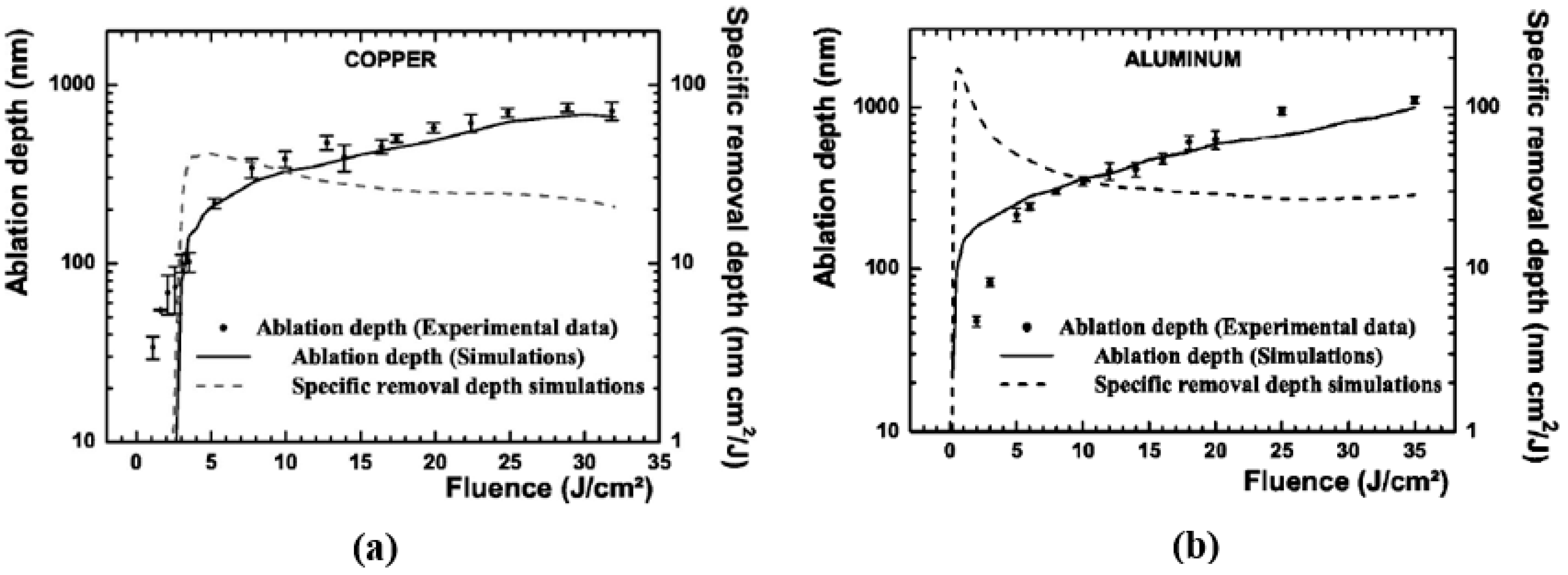
Specialised models were also developed to investigate specific physical mechanisms pertaining to laser–material interaction. For instance, to better understand and predict fs--laser--induced ablation during fs-laser-based processing of materials, numerical and theoretical models were developed. These included molecular dynamics [117,118] and hydrodynamics models [119,120] (continuous thermodynamics model). Predicted ablation depth, using a hydrodynamics model, for copper and aluminium subjected to an fs laser is shown in Figure 5. This figure shows a relatively good correlation between the experimental and numerical results, underscoring the importance of numerical models. The molecular dynamics models include the kinematic equations of each atom present in the ablation entity. Whereas the hydrodynamics model uses a set of equations in a Lagrangian form that represent hydrodynamics along with the multiphase equation of the state. Though these models are able to represent the underlying physics of the process, they are complex and consume large amounts of computational time.
To study the complex process of ablation and to predict the non-equilibrium temperature distribution between the lattice and electrons regime, while avoiding the computational complexities of hydrodynamics and molecular dynamics models, a two-temperature numerical model was developed by Anisimov et al. [121]. Due to the fact of their computational efficiency, two-temperature models (TTMs) are widely used to model fs laser processing of metals [99,122]. The two-temperature model was developed from the Boltzmann equation and is composed of the following coupled PDEs (partial differential equations) [123]:
C e ( T e ) T e t =   K e 2 T e G ( T e T l ) + Q ( r , t )
C l T l t =   K l 2 T l + G ( T e T l )
where C e is the electron heat capacity, C l is the lattice heat capacity, K l is the lattice thermal conductivity, K e is the electron thermal conductivity, Q ( r , t ) is the laser energy density absorbed per unit time, and G is the electron–phonon coupling constant. In these equations, the temperature-dependent variables are G , K e , and C e . Equations (1) and (2) represent the mechanics of heat transfer in the electron and lattice reservoirs, respectively, and they are composed of the diffusion equations for both reservoirs and the coupling term that represents the temperature difference between the two (i.e., electrons and lattices). Accordingly, these are the energy balance equations that represent the absorption of the laser pulse by the metal. The basic TTM, represented by Equations (1) and (2), has been subjected to various modifications and adaptations, to increase its accuracy or investigate a particular physical interaction.
TTM was adapted to account for additional physical properties. For instance, Ahmed et al. [124] developed a numerical model to simulate fs laser ablation of copper. In this effort, a TTM model that accounts for the thermophysical and dynamic optical properties was used. The important process parameters considered in their work included pulse number, laser fluence and the time interval between pulses. The laser pulse chosen was Gaussian with the FWHM mode having a wavelength of 800 nm. In addition, electron temperature and lattice heat capacity were considered in calculating the dynamic thermal properties. For both single- and multi-pulse laser irradiation with varying process settings, numerical simulations were carried out. It was concluded that during ablation of copper, while keeping the fluence constant, the ablation depth increases with the increase in the number of pulses.
Attempts were made to implement TTMs in commercial modelling packages that could enable a wide range of users to model laser–material interactions. For instance, Lee et al. implemented a TTM in the finite-element-based commercial software ABAQUS [125,126]. Temperature predictions obtained by the implemented model were validated using analytical results of the linear two-temperature model. The low and high fluences were also validated using nonlinear simulations and data values taken from literature [123]. The overall research concluded that a pulse repetition rate in the range of 0.1–1 GHz aids in maximising ablation and reducing melt pool generation. The latter two conditions enabled a more precise metal cutting process [125,126]. Limitations and potential improvements to TTMs attracted the interest of the research community. For instance, Jian et al. analysed an existing TTM and found that it was limited only by low fluence, which is used for the estimation of important parameters such as electron heat capacity and reflectivity [127]. To improve the prediction of the existing TTM, some parameters, such as electron relaxation time, absorption coefficient, electron heat capacity, reflectivity and electron conductivity, were introduced. The modified model was used to predict the initiation of melting in gold metal and to study the effect of pulse duration on predicting the fluence threshold for initiation of damage [127]. Davydov et al. also attempted to improve the accuracy of TTMs using a semi-empirical equation for the state [128]. However, this approach was less efficient than Jian et al.’s model [127]. A TTM was also modified and used to investigate the effect of the angle of incidence. For studying the temperature and ablation depth during the ablation of copper at an oblique angle of incidence using an fs laser, a numerical simulation was developed by Dasallas et al. [129]. The used model was an improved model of the TTM. Improvements included accounting for laser spot size, laser fluence and the dynamic changes in the reflectivity of the target. Simulation results showed that threshold energy of ablation was highly dependent on the angle of polarisation and the polarisation of incident light. However, the model did not predict the topography of the crater ablation in detail. TTM-based simulations were found to be useful in studying rapid melting and solidification using laser-based processing. Kuo et al. used a TTM to study the melting and solidification of materials using ultrafast lasers and found that if pure conduction is considered, after turning off the laser pulse, melted layers near the heating surface will solidify [130]. Fischer et al. [131] and Konrad et al. [132] conducted similar investigations but for SLM of metal powders using ultrashort pulses. A one-dimensional TTM that considers the thermophysical properties and temperature-dependent material properties was developed by Cheng et al. to study and simulate fs-laser-induced melting of copper nanoparticles [133]. This model included the extended Drude model with dynamic optical properties. The model was successfully validated using experimental results [52]. Cheng et al. [133] also experimented with fs laser processing of silver nanoparticles and simulated the sintering process using TTM. Jia et al. developed another one-dimensional TTM and used it to investigate the dependence of ablation depth in gold, copper and aluminium on various process parameter settings [134]. In this model, the spatial temperature distribution of the lattice was used to determine the ablation depth. Both TTM- and molecular dynamics (MD)-based models have been used to model laser–material interaction for ultrafast and ultrashort pulsed lasers. However, each approach has its advantages and limitations [135]. For instance, MD better represents the underlying physical interactions, while TTM is less complex and computationally demanding, and it is more compatible with widely used modelling software. In order to overcome the individual limitations of each method, hybrid models that better represent the underlying physics of laser–material interactions were developed. Hybrid models comprising the advantages of both TTM and MD were used to study laser–material interactions for processes utilising ultrashort lasers [136,137].

4. Femtosecond Laser-Based Additive Manufacturing—Powder Bed Fusion

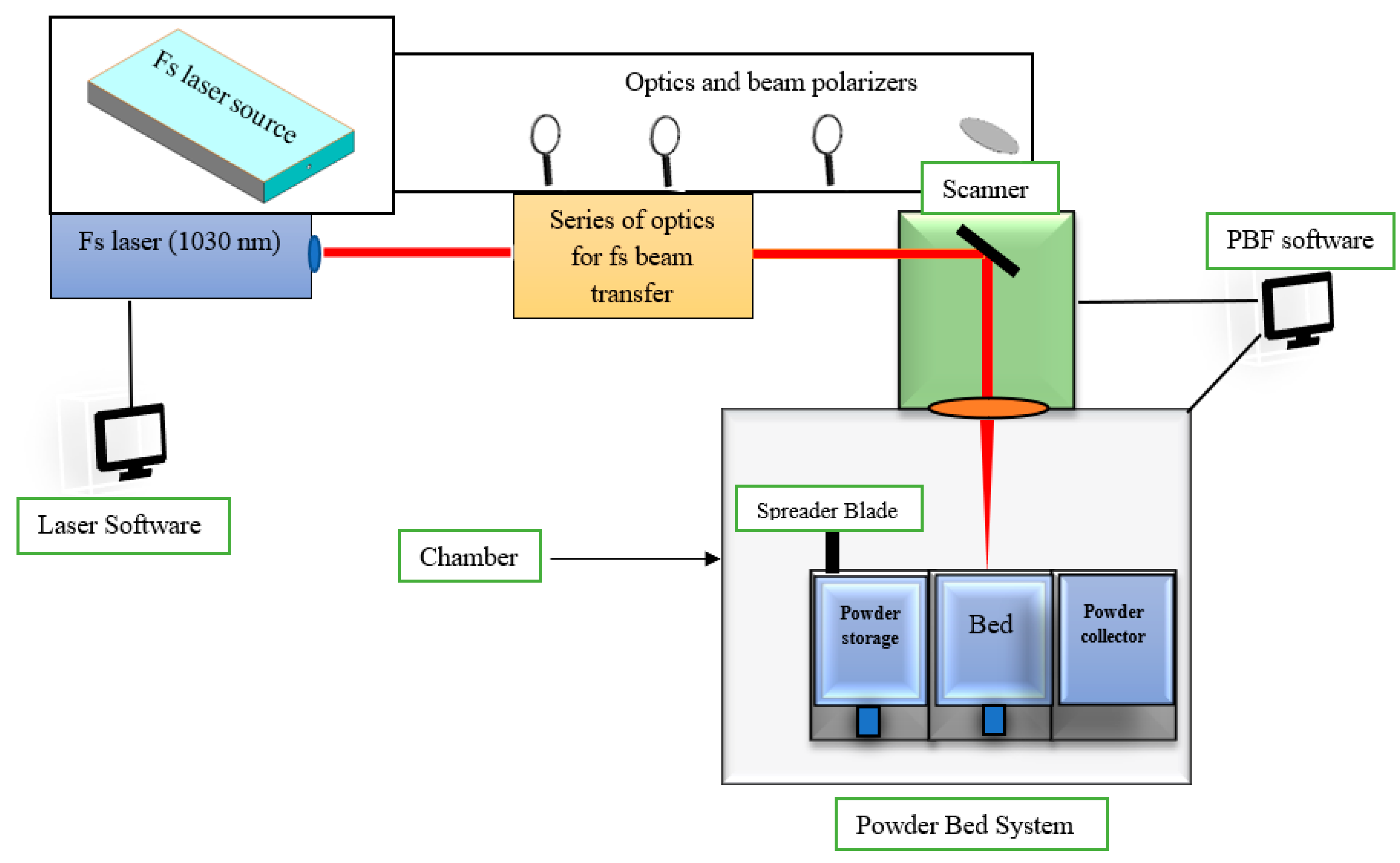
As mentioned previously, the use of ultrashort pulsed lasers in AM results in lower thermal damages to the surrounding environment due to the high peak intensities and short pulse duration. Those result in rapid transfer of energy into the material, causing ionisation that is much quicker than plasma expansion (in the range of ns) [44]. Fs lasers in AM have been employed mainly in two processes, namely, PBF and DW technology. The DW technology is explained in detail in Section 5, and Figure 6 shows the overall schematic of an fs laser source integrated with PBF, i.e., (SLS/M).
The main heating or melting source element during fs laser processing is the fs laser source that is usually operated by the inbuilt laser software. Through this software, laser parameters, such as pulse duration, pulse repetition rate and beam profile, can easily be controlled. When laser parameters are set and the laser beam is allowed to pass through a series of optical elements, the beam is directed towards the scanner system. The required average output power is usually regulated by the beam polariser. The scanner software is utilised to set the scanning speed, hatch spacing, part geometry and the other aspects of the 2D drawing. The laser light is then focused through the scanner onto the powder bed system. The powder system consists of a spreader, powder bed, powder storage and powder collector. Before the laser light falls on the powder bed, the recoater mechanism spreads the powder on the powder bed with a set layer thickness. Then printing is conducted layer by layer. The PBF system could be enclosed in a chamber with an inert gas environment to eliminate oxidation issues. By employing further optimised parameters in fs laser AM, successful manufacturing of more precise functional parts for diverse applications, such as in the microelectronics, aerospace, automotive and biomedical industries, have already been demonstrated [130].

5. Femtosecond Laser Additive Manufactured Powder Materials, Print Qualities and Characterisation

As discussed earlier, laser-based AM has shown great potential in the last few decades for fabricating complex 3D geometries with diverse functional materials and with relative ease. Continuous wave laser-based 3D printing has been the industry standard in the field of laser additive manufacturing. However, and despite the significant advantages associated with the use of CW lasers, there still remain challenges related to heat affected zones and the development of cracks that tend to result in defective parts with poor quality. Many research and development efforts focus on optimising the CW laser processing parameters and conditions to address these issues. More recently, the use of ultrafast femtosecond lasers (pulse duration = 10−15 s) in SLS/SLM (PBF techniques) [54,138] and DW technology [52,53,139,140] is being considered. The use of short laser pulses reduces the developed thermal gradients and would, consequently, reduce the heat affected zones and limit thermal stress levels (associated with the development of cracks during printing). In addition, the smaller spot size in femtosecond lasers allows for a greater precision in the submicron range. Such accuracy and resolution are not typically offered by CW laser systems, which have spot sizes in the mm range. Some of the most recent developments in fs-based AM are discussed below. As different materials bring along different sets of challenges and requirements, this review is presented in sections based on the considered base metal for fabrication. Combined, the sections below provide a comprehensive review of relevant works on fs laser-based AM.

5.1. Femtosecond Laser Sintering of Copper

Copper and copper alloys are widely utilised in industry because of their remarkable properties such as thermal, electrical and corrosion resistance [141]. The utilisation of this metal in AM has diverse applications in various sectors including electronics [142], aerospace [143], automotive [141], heat exchangers [143] and MEMs [142]. Due to the high thermal conductivity of copper (i.e., 400 W/m·K), this material has historically been considered as one of the most difficult to print due to the large heat dissipation into the substrate [143], which prevents a sufficient temperature rise to melt the powders during printing. Additionally, sintering copper-based materials has been reported to be challenging with CW laser sources due to the fact of its high reflectivity that reduces effective energy deposition into the material [144]. Nevertheless, various attempts with certain levels of success have been reported in the literature for AM of Cu-based materials. For example, Pogson et al. [144] investigated the sintering of pure copper through PBF process utilising CW and ns lasers but failed to produce high-density parts [144]. Sciammarella et. al. [145] fabricated 12 cubic mm volume of C1100 copper onto a 4142-steel substrate utilising CW laser at a 900 W laser power [145]. NASA has also reported the successful fabrication of the first full-scale copper rocket part utilising AM methods and copper-based alloys [143]. NASA further fabricated combustion chamber liners, integral channels and closeouts with a high conductive and high-strength copper-alloy i.e., GRCop-42 (copper–chrome–niobium) utilising the PBF (SLM) process [143,146]. Cu–Cr–Zr–Ti alloy powders were also used in the SLM process to produce parts that have applications in the combustion chamber liner of a rocket engine and as heat sinks of the components of the first wall and diverter of the international thermonuclear experimental reactor (ITER) [147]. In addition, Colopi et al. [148] utilised a 1 kW CW laser to fabricate a heat exchanger consisting of complex geometries and fine critical features, where the use of high power was meant to overcome the limitation of poor laser absorptivity [148].
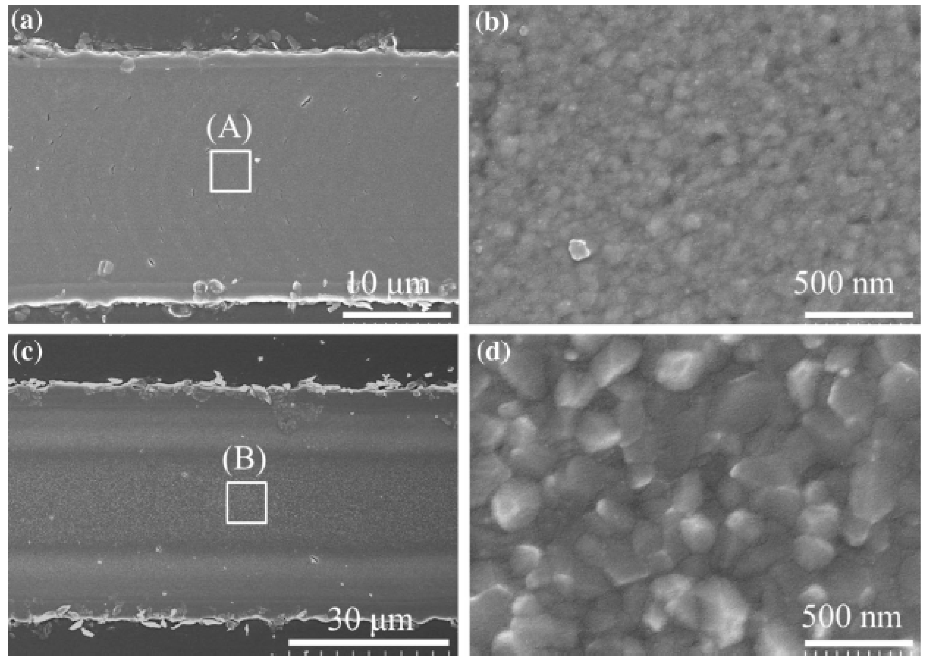
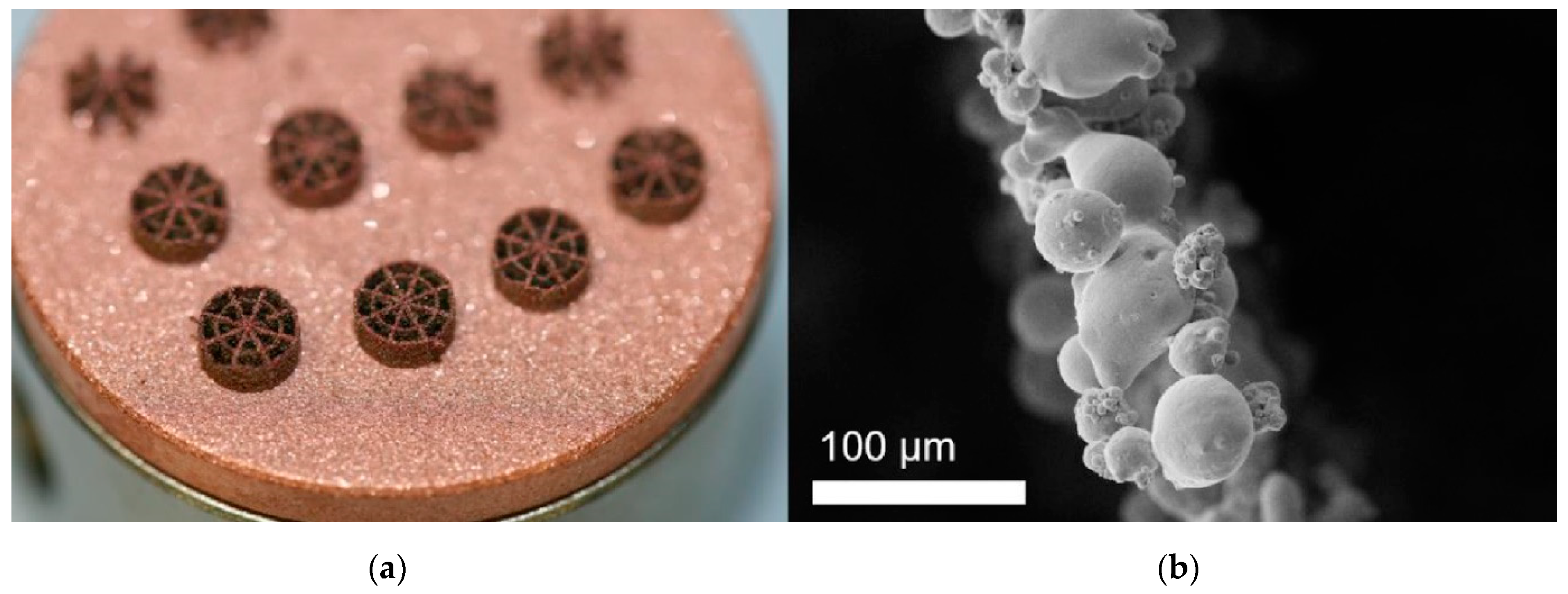
In the current era of the fourth industrial revolution, and with the growing demand for functionality and performance in MEMs devices, an increasing number of transistors must be packed and interconnected on electronic boards, resulting in smaller chips and interconnects [141,148]. To fabricate transistors and interconnects, traditional manufacturing techniques have been utilised. However, the fabrication of miniaturised features using such traditional techniques is limited [142]. Currently available macroscale metal AM techniques, such as PBF utilising CW lasers, are reported to produce a minimum feature with sizes up to 100 µm, which is still too large. The minimum feature size of a back-end-of-line (BEOL) wafer interconnect is in the range of 15–20 µm [149]. To address this issue, nowadays, a new technique called microscale AM is being employed to fabricate parts at the micro- and nanoscales. The DW process is a widely used AM technology for such microfabrication of conductive micropatterns using Ag, Au and Cu metals [150,151]. Among these, Cu is considered to be the key material for low-cost printing [152]. Further, the ultrafast lasers, such as ns and fs lasers, are preferred over CW lasers in micro-level fabrication because of the smaller spot sizes, lower HAZs, and less substrate damage [149,153]. Copper has been most widely in fs laser sintering due to the fact of its wide range of applications in MEMS [116], microsensors [53], complex cooling structures [138], among others. Cheng et al. [52] demonstrated experimentally and theoretically the sintering of copper nanoparticles (NPs) utilising a femtosecond laser. The fs laser sintering was carried out on a copper-coated substrate with a pulse repetition rate of 80 MHz, pulse width of 100 fs and a wavelength of 800 nm. Figure 7 shows SEM images of copper patterns generated at two average powers of 195 and 210 mW, and a scanning speed of 0.1 mm/s [52]. The experimental and theoretical results for copper nanoparticles sintered by fs laser reported by Cheng et al. were found to be in good agreement demonstrating the great potential of this technique in the field of micro- and nanoscale manufacturing.
N Roy et al. (2017) utilised microscale SLS techniques to investigate and compare the processing capabilities of CW, ns, and fs lasers to achieve miniaturised features of 1 µm sized interconnect transistors [142,149,150]. The oxidation issues were reported to be more severe in CW laser sintered parts compared to the ns and fs laser sintered parts. The HAZs were also minimal and there was lower substrate damage for the ns and fs lasers compared to CW laser sintering [142]. Mizoshiri [53,152] utilised an fs-laser-based DW additive manufacturing process to fabricate copper-based microsensors for temperature sensing. This was achieved through reductive sintering of CuO. In this experiment, Cu2O-rich sensing parts and Cu-rich electrodes were 3D printed. Though laser reductive sintered metal oxide NPs were reported to have higher resistivity than laser sintered metal NPs, their absorption of irradiated light was higher [152]. Figure 8 shows the Cu NPs spin-coated substrate irradiated with a femtosecond laser to form Cu- and Cu2O-rich micropatterns. The film was spun-coated at 7000 rpm on a substrate with a thickness of 1 mm with different materials, i.e., CuO NPs at 60 wt%, ethylene glycol at approximately 27 wt% and PVP solution at approximately 13 wt%, respectively. Later, the unsintered part was removed by ethylene glycol and ethanol.
As for the laser processing parameters, a pulse repetition rate of 80 MHz, pulse duration of 120 fs and a max pulse energy up to 0.62 nanojoules, operating at an 800 nm wavelength, were used [53]. It is evident from Figure 8e, that in the case of both the glass and the PDMS substrates, the width of the printed lines decreased with the increase in the scanning speed. In addition, the authors noted that at a particular scanning speed, the line width on the PDMS substrate was broader than on glass. This was due to the higher thermal conductivity in the case of the PDMS substrate. Cu, Cu2O and CuO were present in all of the sintered micropatterns. The micropatterns, characterised using XRD, showed that the Cu peak was stronger at a 5 mm/s scanning speed compared to a 1 mm/s. The ratio of Cu2O to CuO peak intensities in the XRD spectra of the sintered sample was considered to evaluate Cu2O generation. According to the XRD spectra, the maximum Cu2O generation occurred at a scanning speed of 1 mm/s. Therefore, the Cu2O-rich sensing part of the micro-temperature sensors has been demonstrated in this paper under these conditions. Therefore, in the aforementioned work, Cu-rich and Cu2O-rich micropatterns were selectively fabricated by optimising the laser parameters [53]. This work paves a new way for better manufacturing techniques utilising fs laser reductive patterning for the manufacturing of microdevices. Mizoshiri et al. [154] further investigated the effect of various parameters, such as scanning speed and laser fluence, during fs laser reductive sintering of NiO and CuO mixtures on heat accumulation during sintering. It was identified that short pulsed laser irradiation at higher fluence reduces the metal oxide content in the fabricated pattern. Further, n-type and p-type thermoelectric micropatterns were fabricated using fs sintering, which may serve as metal electrodes in flexible displays.
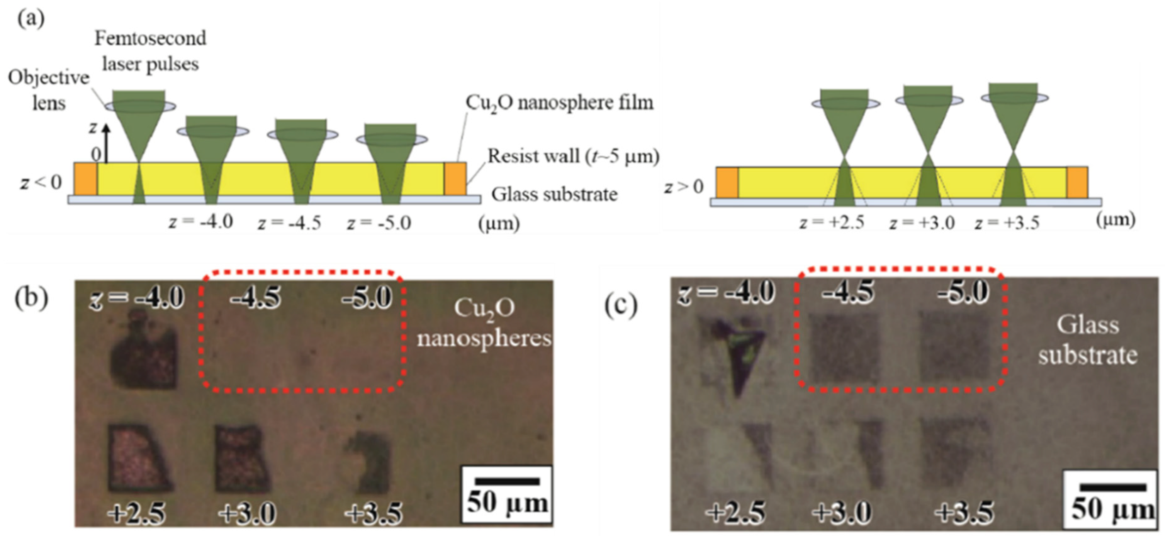
Figure 9 depicts the surface morphologies of the micropatterns sintered at various scanning speeds while keeping fluence constant at 0.059 J/cm2. At lower scanning speeds, more pronounced ablation was observed. Furthermore, at scanning speeds of 5 mm/s, instead of full melting, the powder particles were properly sintered. It was discovered that even when the fluence was kept constant, the scanning speed could affect the content of the Ni and Cu percentages in the sintered micropatterns. It was further mentioned that Cu converts to CuO when temperatures rise above 673 K [154]. When compared to the single exposed sintered sample, the double-exposed sintered sample contained more metal oxides. The heat accumulation and thermal history (single or multiple times exposed) during sintering are important in determining the composition and thermoelectric properties of the sintered sample [155]. Similarly, by utilising near-infrared fs laser pulses, three-dimensional copper-based microstructures were fabricated [156,157,158]. Mizoshiri et al. [158] expanded their research and printed Cu-based micropatterns inside Cu2O nanosphere films using a femtosecond laser. To minimise the thermal diffusion, the line width was maintained to be the same as the diameter of the laser spot, i.e., 0.7 μm. Copper-based microstructures were printed via thermochemical reduction of Cu2O by varying the focal plane along the z-axis, and the laser spot was focused inside the Cu2O film (Figure 10). Different micropatterns have been demonstrated by varying the focus spot in the z-direction as shown in Figure 10. The laser peak intensity was set at 204 GW/cm2 and the scanning speed was 0.01 mm/s [158]. Square micropatterns of a size 1.8 × 1.8 mm2 were fabricated at a laser peak intensity of 163 GW/cm2 and a scanning speed of 100 m/s.
Mizoshiri et al. [152] carried out laser-reduced sintering patterning in an inert gas (N2/Ar) environment and were able to produce lower copper oxide (CuO/Cu2O) generation in the fabricated sample. They used a pulse duration of 120 fs, a laser wavelength of ~780 nm, a scanning speed from 5 to 10 mm/s, a pulse energy of 0.74 nJ and a pulse repetition rate of 80 MHz [152]. Their investigations revealed that as the injection rate of inert gases (N2 and Ar) increased, lower metal oxides were produced, but the fabricated samples had lower surface densities. The XRD results show that the fabricated pattern was greatly reduced (i.e., Cu rich) and the degree of reduction was maximised at a scanning speed of 8 mm/s. Furthermore, the Cu generation in the composition of the fabricated pattern increased with the rate of gas injection, while the degree of reduction was unaffected by the type of gas (N2/Ar). However, as the gas injection rate increased (i.e., higher than 100 mL/min), the porosity in the patterns increased. Using fs laser reductive sintering, the copper micropatterns could be fabricated with a much lower pulse energy of approximately 0.5 nJ and a lower average power of approximately 50 mW, but, in the case of CW and nanosecond pulse lasers, a minimum of 0.2 W would be needed.
Although DW technology has been successful in producing Cu micropatterns using the fs laser sintering technique, the process appears to be time-consuming, requiring the preparation of film coated on substrate, sintering and, finally, removing the unsintered area from the substrate. However, in the PBF process, using layer-by-layer sintering, 3D structures can be produced that could have applications in cooling structures and heat exchangers. Kaden et al. [54] demonstrated printing of copper by PBF process, i.e., printing layer by layer utilising an fs laser with a 1030 nm wavelength and a focal spot of 35 µm [54]. The experiment was carried out in a nitrogen gas environment. Powder layer thickness was maintained manually at approximately 30 micrometres using a squeegee. The results were benchmarked and compared with different repetition rates utilising the energy per unit length (line energy) given by:
Line   Energy   ( El ) = P a v g V s c a n   = E p u l s e × F r e p V s c a n
where El is the energy per unit length, Pavg is the average power, Vscan is the scanning speed, Epulse is the pulse energy and Frep is the repetition rate.
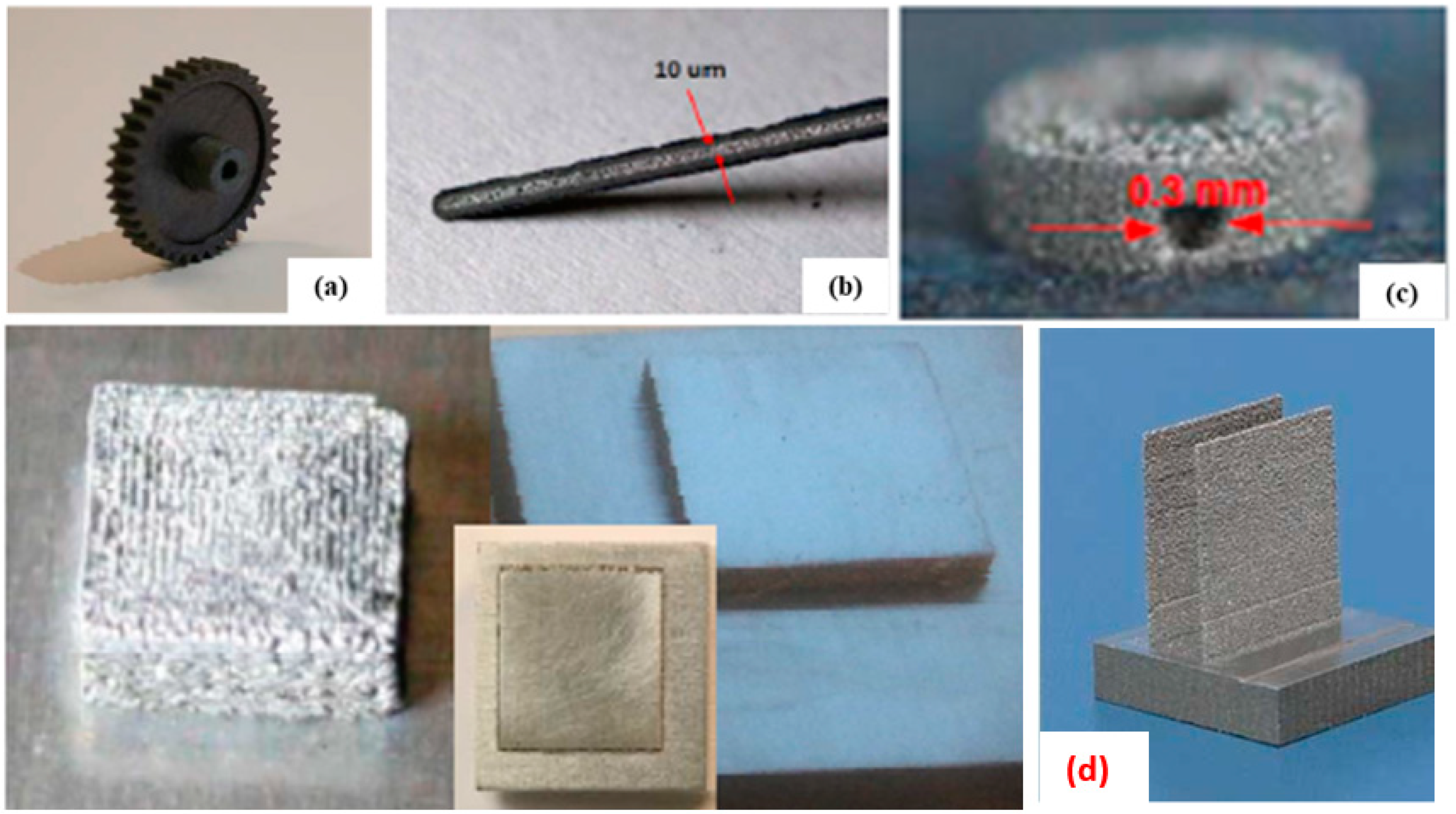
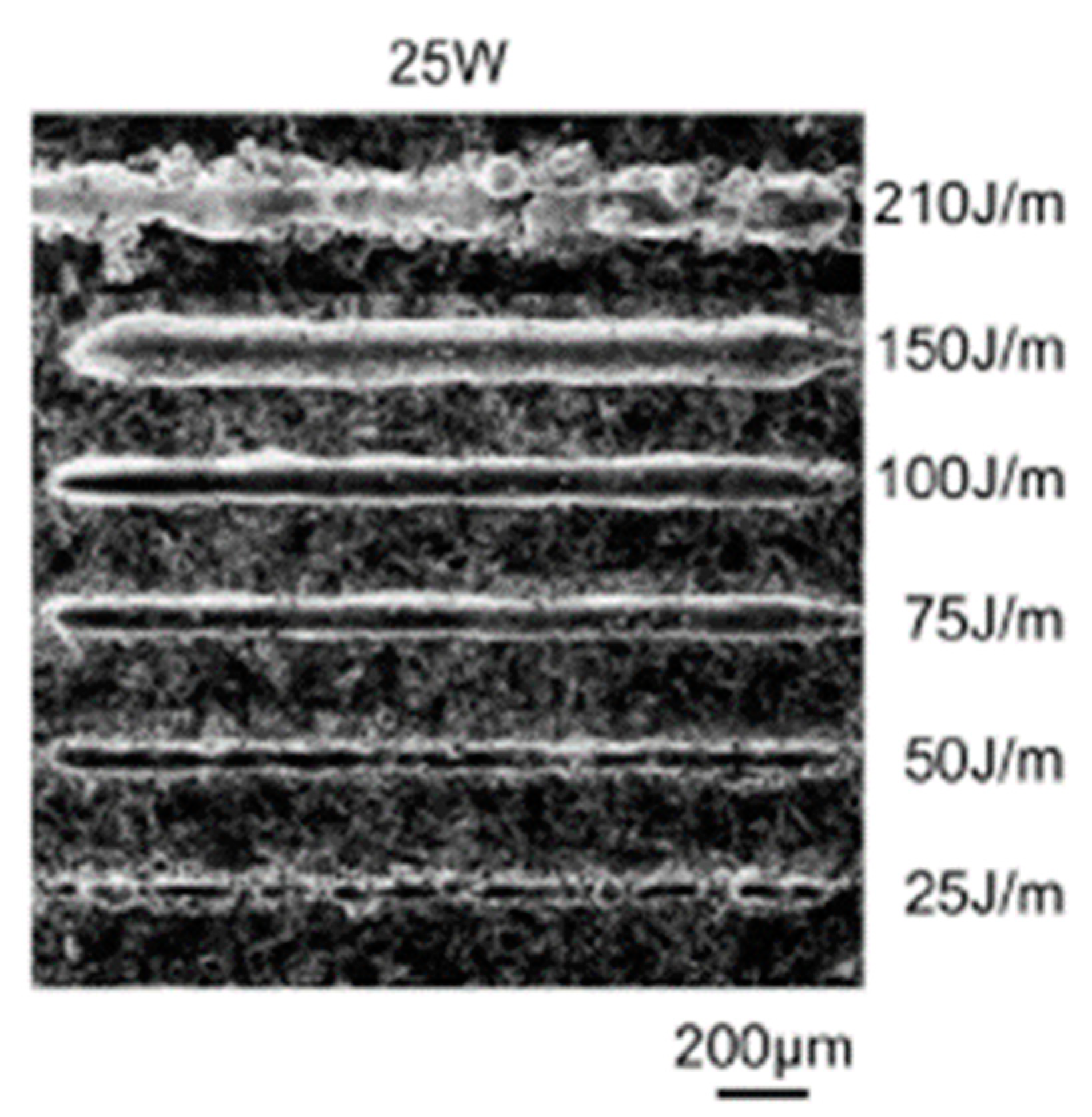
In general, with lower repetition rates, insufficient melting occurs, resulting in poor fusion of the metal particles to the substrate. By increasing the pulse repetition rate to 20 MHz and maintaining the pulse energy to 1 μJ, proper bonding of the copper powder to the substrate has been demonstrated [54]. Blasting and ablation effects were reported when the pulse energy increased by more than 1.5 μJ. It was also found that the thermal accumulation effect could be responsible for successful fusing of metal particles to the substrate at higher repetition rates. The line energy also had an impact on the resulting print quality. Further, printing of thin-walled web-like structures at a scanning speed of 666 mm/s and a pulse energy of 1 microjoule was reported. These thin walls were reported to have an aspect ratio of approximately 15:1 and a thickness of less than 100 μm. Figure 11 and Figure 12 show samples fabricated using fs sintering of copper particles with ultrashort laser pulses. At higher line energies, the HAZ increased significantly which, consequently, negatively impacted the local precision. As a result, the line energy was reported to be kept below 100 J/m in their subsequent experiments [138].

5.2. Femtosecond Laser Sintering of Iron and Tungsten

Tungsten and its alloys have diverse applications in various fields such as lighting engineering, aerospace, electronics, medical, nuclear and military [159,160]. This refractory material possesses exceptional intrinsic properties such as high tensile strength, high hardness, high melting temperature, high density, high thermal conductivity, high recrystallisation temperature and low thermal expansion [159,160,161]. These properties make tungsten ideal for high-temperature, high heat flux applications in radiation environments such as collimators, radiation shields in imaging systems (CT, SPECT, MRI and X-ray) [162], plasma-facing components (PFCs) in future nuclear fusion devices, such as the International Thermonuclear Experimental Reactor (ITER), and high-performance rocket nozzles [159,160,161,163,164]. However, tungsten’s main disadvantage is its lack of room-temperature ductility that restricts its machinability and limits its use as a structural material. The brittle-to-ductile (BDT) transition temperature of tungsten, which is typically between 200 and 400 °C, limits its fabricability [162]. Because of this BDT transition temperature, tungsten products are conventionally manufactured by chemical vapour deposition (CVD), spark plasma sintering (SPS), powder metallurgy (PM) and hot isostatic pressing (HIP). These techniques, however, have limitations when it comes to complex internal and external structures [159]. SLM/S was used to overcome these limitations. Though it was not an easy process in the early stages, since the AM of tungsten is hindered by almost all of the difficult challenges in metal SLM/S processing such as high melting point, high thermal conductivity, affinity for oxygen at high temperatures, high viscosity, and brittle nature at room temperature, resulting in cracks and porous microstructures of fabricated parts [161].
Despite the listed challenges with processing tungsten, successful examples are reported in the literature. For example, Ghosh et al. [165] utilised a pulsed Nd:YAG laser with a pulse duration of approximately 1000 ns to investigate SLS of tungsten carbide and cobalt powder alloys. Porous samples were produced in this experiment. Dianzheng et al. [166] utilised CW laser-based SLM to fabricate pure tungsten material parts with densities of up to 96 percent; however, this was accompanied by some microcracks in the printed components. Chaolin et al. (2018) utilised CW laser to fabricate pure tungsten samples by SLS processes. The produced parts possessed dense microstructures without balling but a few microcracks still existed [159]. Muller et al. (2019) carried out experiments to fabricate pure tungsten powder parts utilising CW laser-based PBF with laser power up to 400 W and by preheating the substrate up to 1000 °C. The produced parts had a relative density of up to 98 percent, and cracks were minimised but not eliminated completely. The same research team also fabricated honeycomb-like structures with tungsten–copper composite materials, which were utilised as heat sink materials for PFCs with high heat loads [164]. Li et al. (2020) investigated various process parameters in CW laser-based SLS, such as scanning speed, hatch spacing and laser power, and their effect on the surface microstructure, densification and morphology of fabricated tungsten samples. With the optimum parameters of a scanning speed of 400 mm/s, hatch spacing of 0.08 mm and laser power of 300 W, the produced tungsten samples had densities of up to 98.31 percent [160]. As noted from the aforementioned studies considering CW laser-based AM of tungsten, and despite the reported success, shortcomings in terms of cracking still represent a challenge. The studies utilising fs lasers aimed to improve the relative density, hardness and strength of SLS/M-produced tungsten parts. The high peak power and the ultrashort pulse duration of fs lasers make them an emerging technology in melting/sintering high-temperature metals such as tungsten [7,44,58,101]. Due to the phenomena of fast cooling, localised heating, lower HAZs and greater precision in the submicron range, these ultrafast lasers have many advantages over CW and long-pulsed lasers. 3D printing of such high-temperature metals would benefit industries, including the automotive, biomedical and aerospace, that require high-temperature materials with outstanding mechanical qualities and accuracy [7].
In an early study, Ebert et al. (2012) initially investigated fs laser processing of tungsten powder and was able to report sintered structures. In these experiments, the fs laser used had an operating wavelength of 1030 nm and 180 fs pulse duration. The laser repetition rate was tuned from 0.125 to 1 MHz, and the laser spot diameter was ~36 microns. The layer thickness was reported to be maintained around 1 mm and was irradiated from 1 to 50 times. The experiments were carried out in vacuum at 0.05 Pa, with helium used as a residual gas during the sintering process [101]. It was reported that when the line spacing was at approximately 0.01 mm, the sintering of continuous surfaces was possible, and the sintered structures were in the range of 1 to 10 μm. The SEM images of the sintered part under different processing settings are shown in Figure 13a–d. These results demonstrate some sintering phenomena utilising fs lasers but do not provide precise and optimum laser parameters on the quality of the sintered structures.
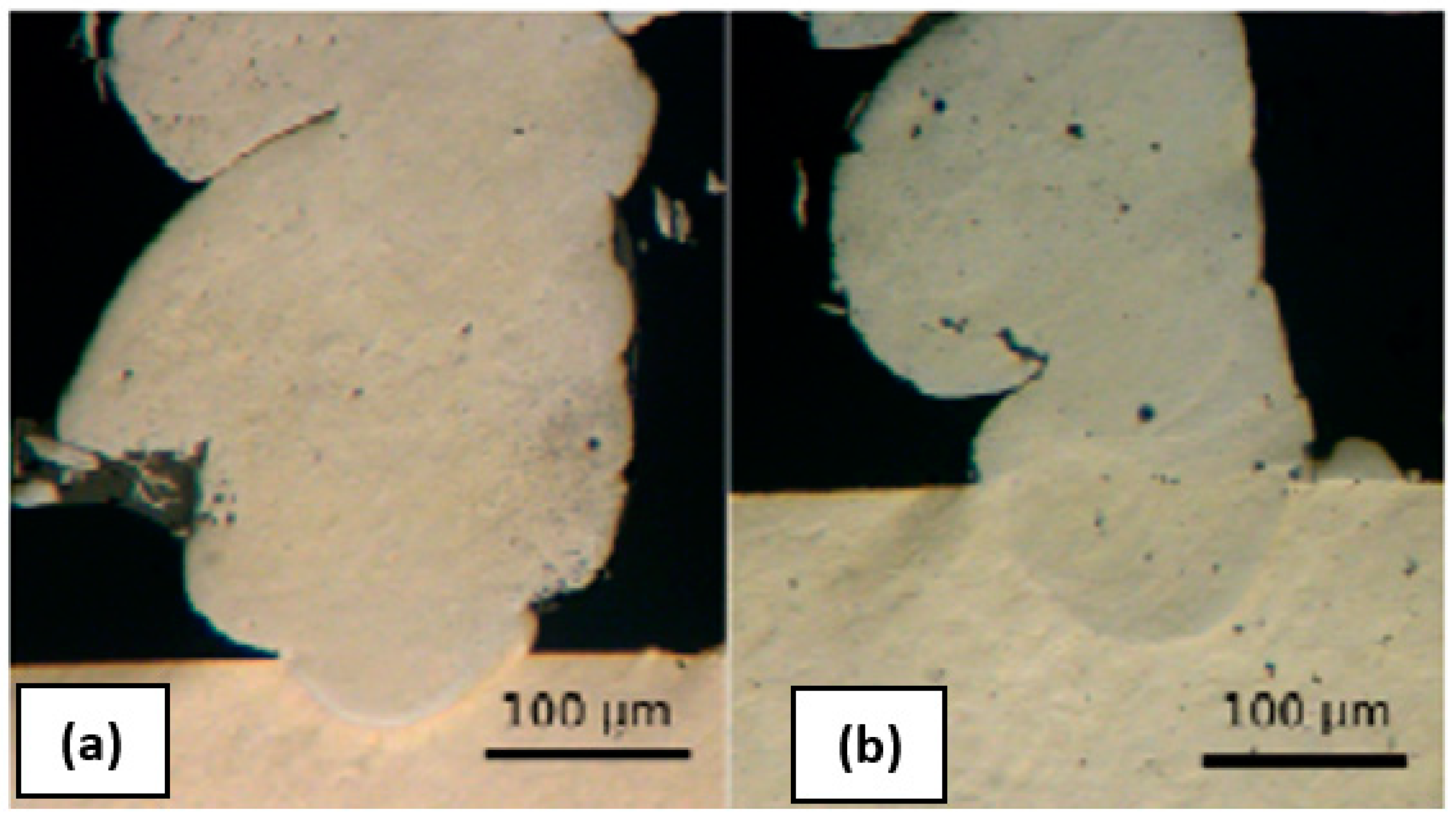
Furthermore, Huan Huang (2015) [7] carried out fs laser sintering/melting experiments with tungsten and iron powders to produce 3D structures fused to the substrate. To compare the mechanical properties and microstructure of fs-laser-fabricated samples, similar 3D structures were fabricated using a CW laser source while maintaining the same average power of 50 W, and the scanning speeds for both the CW and fs pulse lasers operated at 80 MHz. The particle sizes of the iron and tungsten powders were in the range of 1–5 μm. For analysing the properties of the printed structures, the 3D printed samples were vertically cut as shown in Figure 14.
The penetration depth of the fs-laser-fabricated iron-powder sintered sample was approximately 30 μm, while the penetration depth of the CW fabricated sample was 75 μm. This difference was attributed to the smaller HAZ in the case of fs laser-based 3D printing. Using the same 50 layer printing, the size of the sample fabricated using an fs laser was 0.8 mm tall, with a wall thickness of 300 μm, and the sample size fabricated using a CW laser was 1.03 mm tall with a wall thickness of 380 μm. This paper demonstrated how localised heating in an fs laser can result in the precision printing of 3D structures. Furthermore, the microhardness of the fs-laser-fabricated iron sample was higher than that of the CW-laser-fabricated sample, because the average grain size in the fs-laser-fabricated sample was smaller at all heights compared to the CW laser 3D printed samples. This is due to the well-known fact that hardness increases as grain size decreases. The grains in CW-laser-fabricated samples were reported to be slightly bigger due to the lower cooling rates and greater HAZs [57]. The next challenging material, tungsten, was fabricated in cube structures by the same research group [7]. With tungsten’s higher melting temperature compared to iron, 1 MHz pulse repetitions at 45 W, a pulse duration of 400 fs, a layer thickness of 15 μm and scanning at a speed of 25 mm/s yielded strongly fabricated parts fused to the substrate (Figure 15). On the other hand, 80 MHz fs laser and CW laser operating at higher power failed to completely melt and fuse tungsten powder to the substrate.
The mechanical properties, such as average ultimate tensile strength (388.4 MPa), were determined from three sample locations. However, because of the porosity and potential oxidation during 3D printing, the microhardness values were reported to be unsatisfactory. Further, three-dimensional structures utilizing tungsten material were fabricated [44]. Different tungsten samples, including 100 μm thin walls, were 3D printed using fs laser source as shown in Figure 16 [44].
For comparison, 20 ps and 200 ps pulsed lasers as well as a 750 fs laser and a CW laser system were employed in the 3D printing of tungsten [44] while keeping all other parameters similar. Figure 17 shows the average grain area versus pulse duration for fs, 20 ps, 200 ps and CW laser sintered samples, where the left is for the top surface and the right is for the cross-section. Comparing the microhardness in the case of pulsed lasers at different durations with the CW laser showed that fs-laser-based AM had the highest hardness as displayed in Table 6.
The aforementioned work also revealed that the fs laser sintered samples had lower cracks and defects compared to the other laser printed samples. Similarly, fs laser sintering of iron powder coated on a glass substrate was demonstrated by Liu et al. (2016) [100]. Melting and fusing both (i.e., iron and glass) materials is challenging because of the glass’ brittleness and the different thermal expansion coefficients of iron and glass. In this study, the fs laser was utilised to overcome this issue, because of its localised heating, high temperature generated in a shorter time and quick cooling rate, The sintering parameters, such as average power of 37 W, powder layer thickness of 40 μm and 20 μm line spacing were used during the sintering process at various scanning speeds [100]. The reflectance was measured for the fabricated samples at different values of the laser power and scanning speeds. It was found that at lower scanning speeds, the reflectance was reduced, while noting that glass was prone to breaking at lower scanning speeds. The reported findings suggest that fs laser AM could be a new way to achieve an excellent blackening effect with a reflectance of less than 1%, rendering it useful for applications in stray light reduction.

5.3. Femtosecond Laser Sintering of Silver

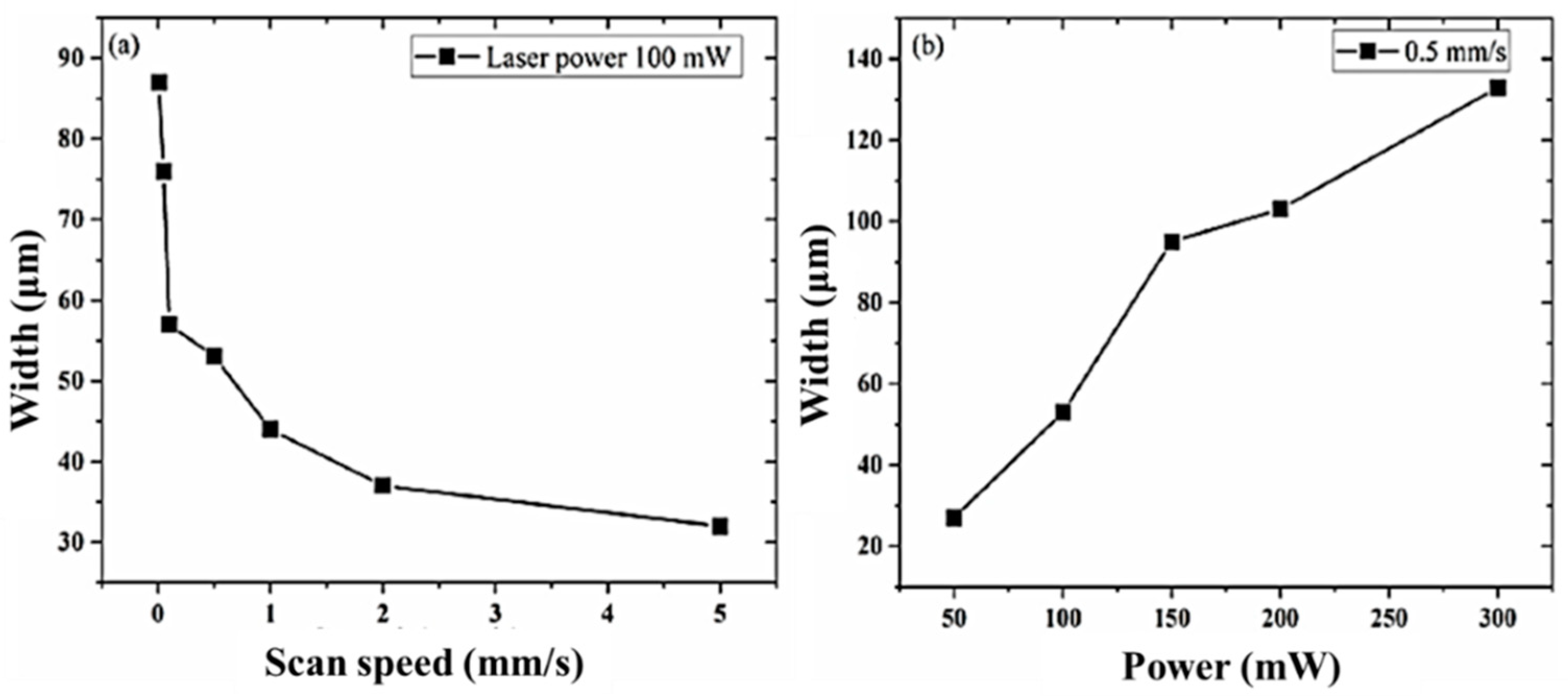
Nowadays, electronics has seen substantial improvements in the field of sensors, printed electronic components and flexible electronics. These flexible sensors are rapidly evolving, where they can be used in many applications [167]. In the medical sector, these flexible electronics have a large impact, as they can be low-cost, tactile, low-weight and non-pervasive wearable systems; in addition, they can be used as monitors to observe patients’ health conditions on a regular basis. Hence, there is an existing special need to manufacture such flexible devices using appropriate manufacturing technology. This can be facilitated by using AM technologies, such as SLS, that can process metal NPs and also in direct writing technology. Initially, the SLS process was used for NPs of noble metals like silver and gold, but later it was also expanded to more cost-effective materials such as copper and nickel [151]. Silver material has been utilised by inkjet technology-based AM process for fabrication of temperature sensors [168,169,170]. Hong et al. processed silver particles via a laser sintering process to fabricate a large and flexible transparent conductor based on microgrid structures that can be used in touch screen panels and optoelectronic devices [171]. In 2011, using direct writing technology, Lee et al. fabricated conductive metal films made out of silver nanoparticles. Femtosecond laser characteristics aid in the fabrication of metal conductors with submicron-sized features and high conductivity. Due to the fact of its reduced HAZ, femtosecond laser-based metal patterns on transparent and flexible polymer substrates has garnered special attention owing to its several practical applications in photonic devices and flexible electronics [41,56,167,172]. Fs laser has also been utilised to fabricate SERS (surface enhanced Raman scattering) substrates [172]. SERS is an analytical tool for detecting molecular fingerprints and integrating them into microfluidic platforms that allow for liquid sample analysis for biological and medical diagnosis. Traditionally, lithographic techniques have been used to produce SERS substrates with significant Raman enhancements. However, fabricating them, on the other hand, entails a number of time-consuming steps. Furthermore, using lithographic techniques to achieve ordered arrays of nanostructures of arbitrary size can be expensive [56], challenging [56], hazardous and incompatible with sensitive substrates [172]. To address these issues, fs lasers have been used to fabricate SERS substrates sintered with silver nanoparticles [56]. Based on the process parameter set and the layer thickness, sintering of nanoparticles may lead to three different phenomena: surface necking, full melting of silver particles and balling. Kurnoothala et al. [56] sintered silver nanoparticles on a silica-based microfluidic channel via the surface necking phenomenon using an fs laser source to fabricate the SERS substrate. The width of the fabricated lines at various laser powers and scanning speeds were reported [56] and are shown in Figure 18. The utilised fs laser system operated at a wavelength of 1030 nm, a 370 fs pulse duration and had a pulse repetition rate of 1 MHz.
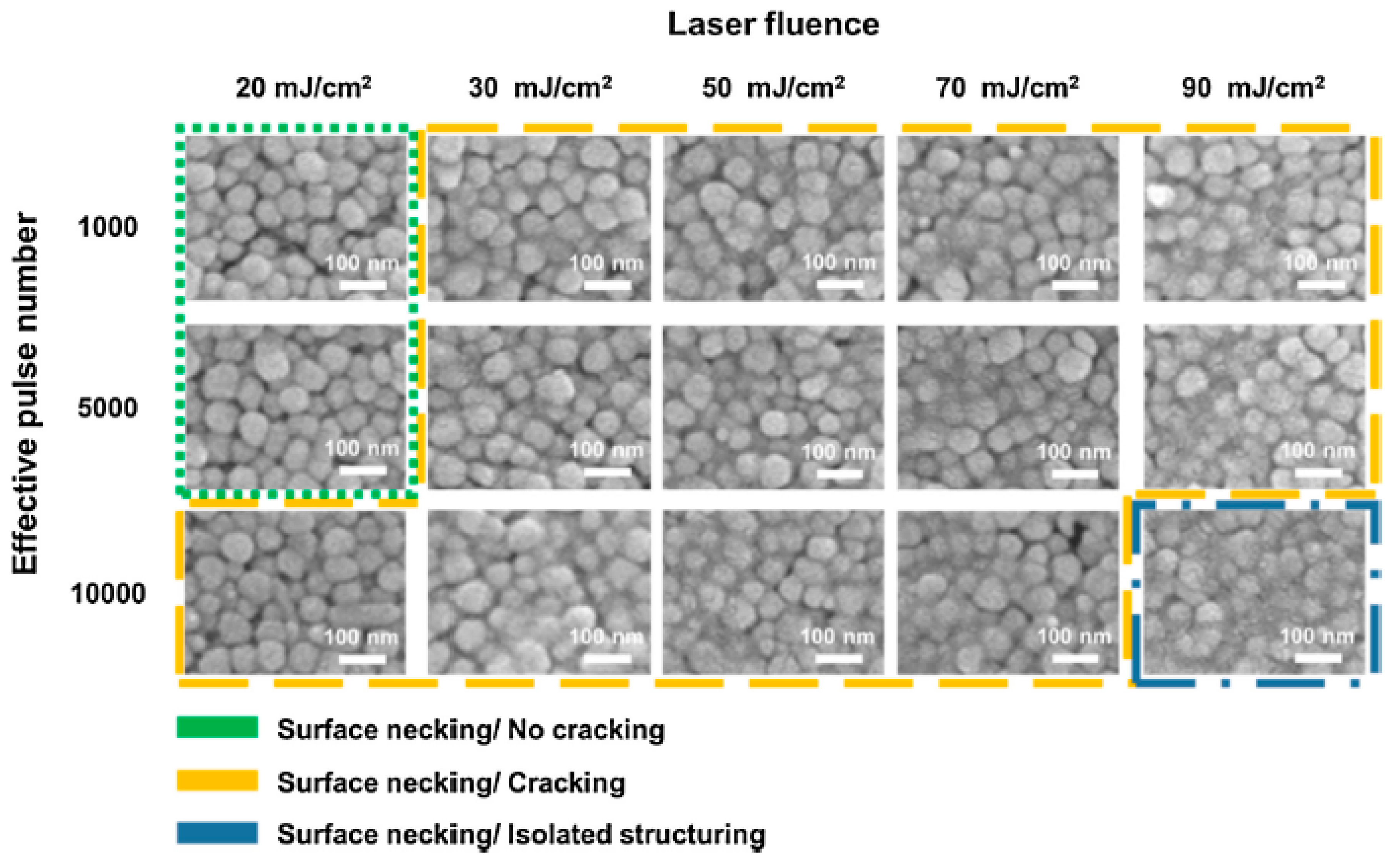
Due to the ultrashort pulse durations in fs laser sintering, the thermal diffusion effect is suppressed, and sintering of metal nanoparticles can be restricted to the laser focal spot. This largely reduces the heat-affected zone and enables the fabrication of submicron-sized metal patterns on flexible substrates [55]. Noh et. al. [173] utilised a Ti:sapphire laser system operating at an 800 nm wavelength, a 50 fs pulse duration and a pulse repetition rate of 1 kHz to fabricate silver NPs on a flexible substrate. The laser fluence and effective pulse number were 10–120 mJ/cm2 and 1000–10,000, respectively. The scanning speed, V, varied between 20 and 200 μm/s, and the beam size was 200 μm. The hatch space between the scanning lines was set to 200 µm [173]. The reported SEM images of sintered microstructures of the Ag NPs on the PET substrates after fs laser irradiation are shown in Figure 19 [173]. Noha et. al. also compared the results obtained with a KrF excimer nanosecond laser operating at a 248 nm wavelength, a 25 ns pulse duration and a repetition rate of 10 Hz. The experiments were carried out with a fluence = 10–40 mJ/cm2 and a pulse number of 1–1000. The effective pulse number was varied by varying scanning speeds in the 0.015–15 mm/s range at f = 10 Hz and d = 1.5 mm [41].
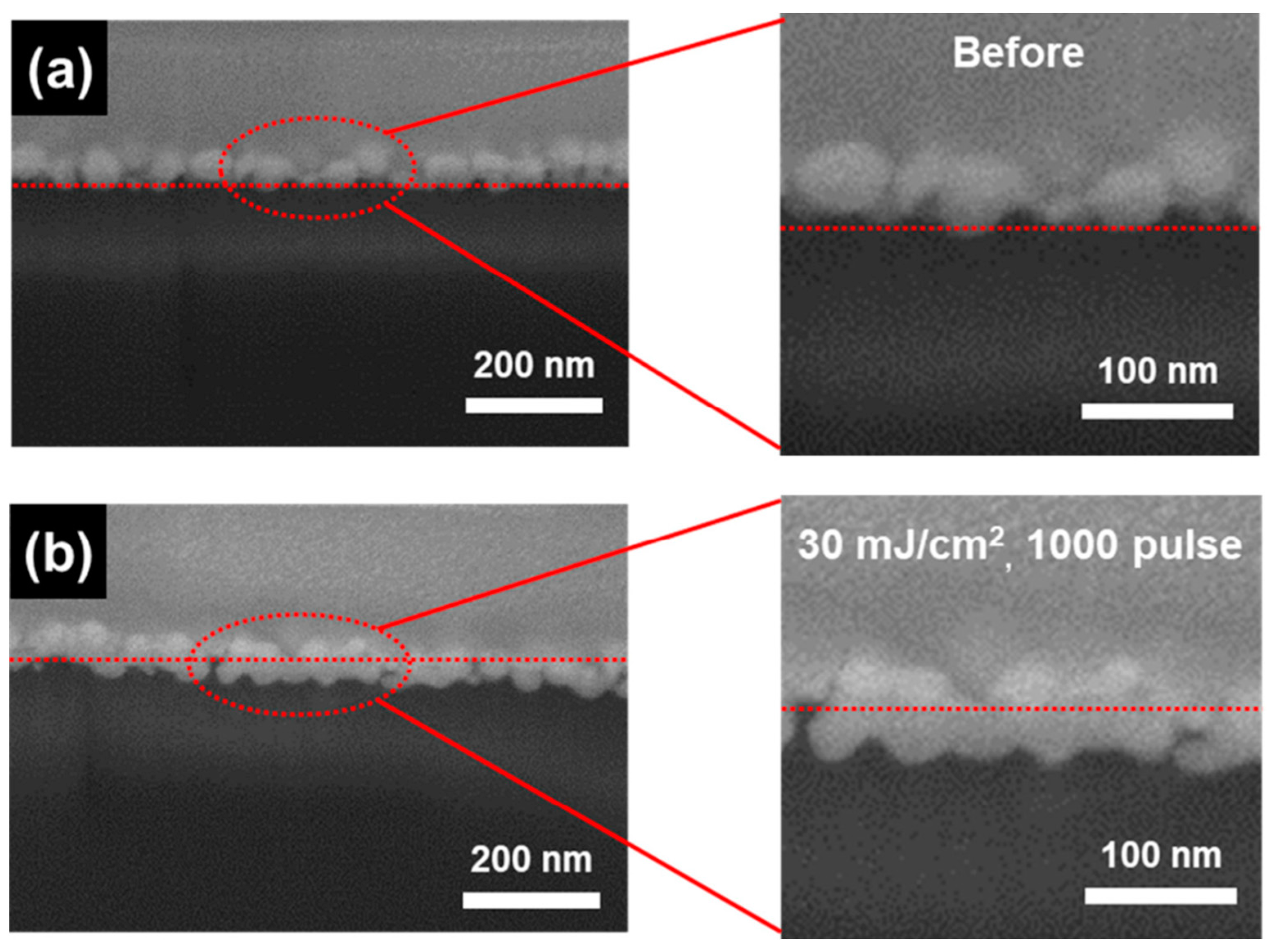
For the entire fluence range reported in [173], fs laser irradiation sintered the Ag NPs without completely melting them, instead creating necks between the particles by solid-state diffusion. As the fluence increased, the significant neck growth arose by grain boundary and volume diffusion. At fluence = 20 mJ/cm2 and an effective pulse number = 1000, the Ag NPs were reported to form necks with an average neck diameter of 12 ± 2 nm. At fluence = 90 mJ/cm2 and an effective pulse number = 10,000, the average neck diameter increased to 36 ± 3 nm. The increased neck formation was reported to reduce the porosity by blocking open pores in the particle bed [173]. As depicted in Figure 20, with the increasing fluence and EPN (effective pulse number), the fraction of the exposed area rose to 40%. This study showed that EPN was less significant in film cracking than laser fluence [173]. It also suggests that the formation of the interparticle necking after laser sintering greatly decreases the electrical resistance. The resistance decreased as fluence and EPN increased until the fluence = 40 mJ/cm2. At a fluence = 30 mJ/cm2 and an EPN = 1000, the lowest resistance was reported as shown in Figure 20c. The mechanical properties of fs laser sintered Ag particles were also examined in this paper for interfacial characteristics between Ag NPs and the PET substrate. The cross-sectional SEM images are also presented as shown in Figure 21 [173].
The aforementioned work reported that fs laser irradiation resulted in substantial embedding of the Ag NPs into the PET layer, which led to an increase in the contact area (Figure 21b) and would significantly improve the adhesion strength [173]. At fluence of 90 mJ/cm2, the embedded depth was found to be approximately half the particle size. Additionally, the reported comparative results of the fs and ns laser-sintered samples showed that due to the low substrate damage and fewer film cracks, fs-laser-generated films were of higher electrical conductivity compared to the ones generated with an ns laser [173]. The surface topography AFM analysis results showed that in the case of ns laser sintering, the average affected spot was 1.2 µm wide and 500 nm deep, whereas in case of fs laser sintering, the average affected spot was 200 wide and 90 nm deep [173].
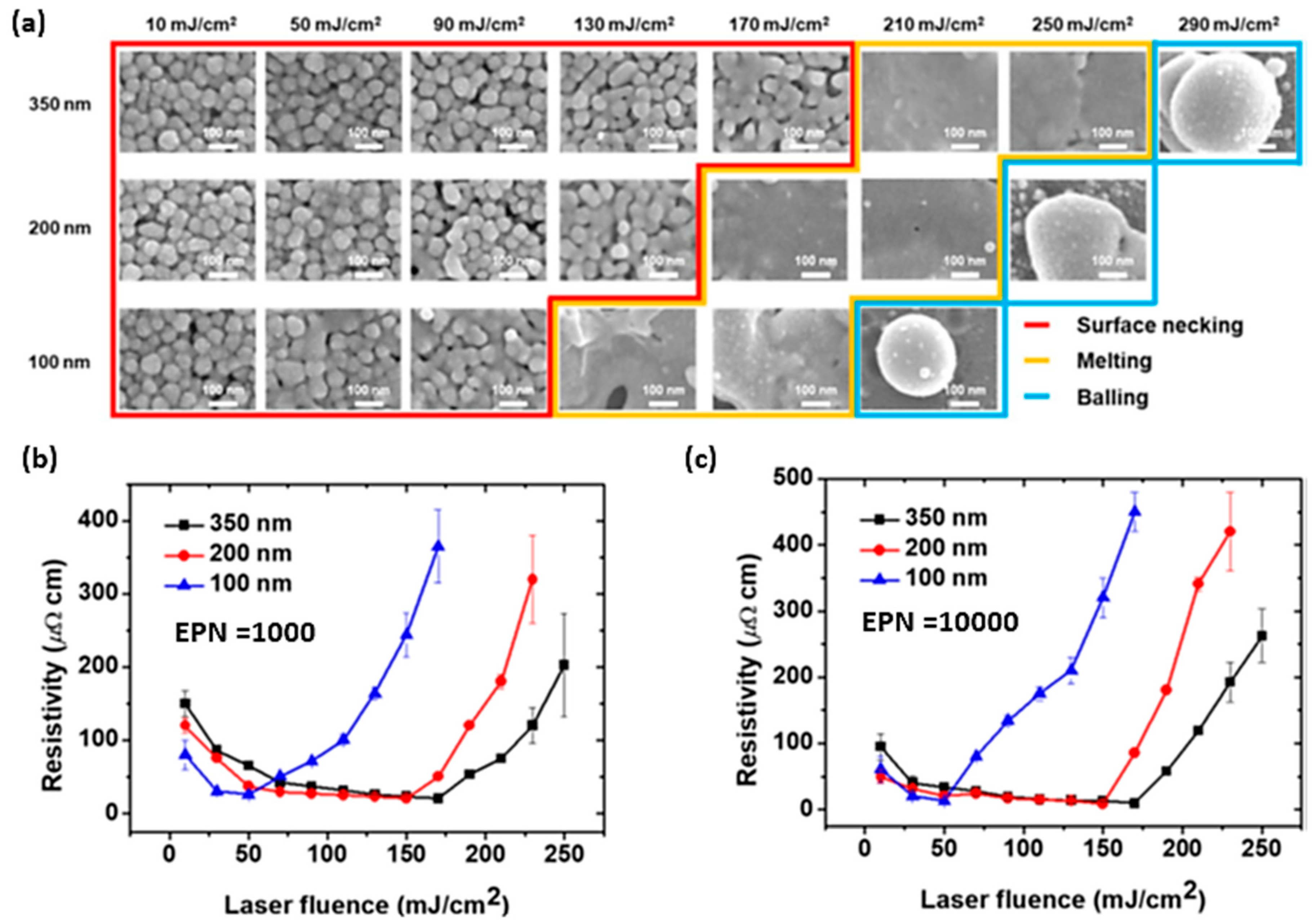
Noh et al. further investigated the correlation between different process parameters and the conductivity, microstructure and adhesion strength of the sintered films [172]. Melting, interparticle necking, balling and film cracking were analysed by varying the EPN, fluence and layer thickness. It was found that both adhesion strength and electrical conductivity increased by increasing the fluence up to the maxim when melting of particles began [174]. By varying the spin-coated layer’s thickness from 350, 200 and to 100 nm, different conclusions were drawn from this study. For the 350 nm layer thickness, short thermal penetration helped in the fabrication of thin-film samples. In the case of the 200 nm layer thickness, the highest thermal conductivity was reported when melting just began in NPs. Whereas with the 100 nm layer thickness, complete melting of particles deteriorated the conductivity due to the capillary instability of the molten film and, therefore, the highest conductivity was reported just before melting started as shown in Figure 22b,c [172]. Moreover, fine patterns of a few hundred nanometre line widths utilising ultrashort lasers were fabricated in other sequel studies [175]. Microstructure formation by varying the sintering parameters of Ag NPs utilising ultrashort pulses was presented and revealed that the fs laser sintering process was similar to typical thermal sintering processes.

5.4. Femtosecond Laser Sintering of Aluminium Alloy

Aluminium is one of the lightest materials that is used for many burgeoning applications such as in automotive parts, electricity lines, defence and aerospace, and food and beverages containers. Conventional manufacturing processes are capable of processing pure aluminium while processing them using SLM is quite difficult. This is because of challenges such as high reflectivity of the laser beam, oxidation and flowability. In addition, pure aluminium has high thermal conductivity compared to its alloys, making it more challenging to fabricate in the SLM process. Additive manufacturing of Al and its alloys has various applications in the automotive and aerospace fields, where fabricating light-weight structures with complex geometries is challenging using other traditional methods [59]. SLM processing of Al and its alloys has been found to be beneficial for hard-to-machine materials. To make Al fabrication possible through PBF process, additives were included [80,176]. Using one of aluminium’s common alloys, AlSi10Mg, parts were fabricated using SLM process. This alloy has a very good hardness and strength and, hence, it is suitable for parts containing thin walls subjected to high loads, especially in aerospace applications [177]. AM-made Al parts are actively used in consumer products [178]. Various Al alloys were processed using the SLM technique including Al6061 and AA2024, among others [179]. These alloys possess good fatigue resistance as well as resistance to stress, corrosion and cracking. In 2010, AlSi12 alloy was processed using the SLM technique to achieve a denser part, but there were oxidation issues [180]. Micromechanical models were developed to quantitatively link aluminium material fracture properties, to microstructure features at multiple lengths scales, and manufacturing conditions [181]. An attempt was made by adding Cu to the Al powders to reduce oxidation, and the control was better when compared to conventional processes [179]. Al–Li alloys are reported to have great potential in light-weight construction, as the lithium content in the alloy significantly increases the stiffness at a lower mass, and the elastic modulus rises dramatically as the lithium concentration increases [59]. However, in traditional casting processes, a maximum Li fraction, up to 2 wt.%, has been reported due to the precipitation of the brittle δ-Al–Li [8]. Recently, it was reported that an ultrashort pulsed laser with a 500 fs pulse duration was used to 3D print the binary element Al–Li with Li content up to 4 wt.% [60]. The high content of Li generated during fs laser 3D printing of Al–Li alloys could be attributed to the high cooling rate within the melt pool during fs laser sintering, which has much shorter laser–matter interaction times. This also, in turn, supresses excessive Li evaporation during sintering. As the Li content increases in the Al–Li alloy, a significant increase in elasticity was found as depicted in Figure 23.
Furthermore, Al 3D parts were printed with an fs laser operating at a 20 MHz repetition rate and a pulse energy of 1.5 μJ at four different scanning speeds (Figure 24). The layer thickness during fabrication was reported to be 40 μm, and the hatching spacing was 30 μm. Complex gear wheels were fabricated by the same research group to prove the feasibility of the fs laser sintering process as shown in Figure 25.
Further, Ullsperger (2017) [38] utilised an fs laser operating at a 1030 nm wavelength, a pulse duration of 500 fs, an average power of 30 W at a pulse repetition ratio of 20 MHz to 3D print AlSi4O alloys. Higher concentrations of Si in AlSi4O served to primarily reinforce the material and to reduce thermal expansion during sintering. Previously, a CW laser was used in additive manufacturing of AlSi4O. However, when the CW laser additively manufactures hypereutectic alloys, such as AlSi4O, low cooling rates cause decomposition due to the low Si solubility in Al and poor precision due to the larger melting zone. To achieve minimal structural sizes, single tracks fabricated by CW laser were reported to be up to 150 μm [182]. To address these challenges, researchers utilised ultrafast laser sources of picosecond and femtosecond pulse durations to fabricate these alloys with reduced HAZs. The 3D printing process was carried out in a nitrogen gas environment to avoid oxidation issues, such that the oxygen concentration in the chamber was below 0.5 percent. The powder bed fusion technique has been utilised, and the powder layer-by-layer spreading was conducted manually with a rubber blade with the layer height maintained between 25 and 50 μm. In the sub-picosecond regime, the single pulse ablation threshold for Al–Si alloy operating at a 1030 nm wavelength was reported to be 0.12 J/cm2 [38]. Ullsperger et al. found that for a layer thickness of 30 μm and at fluence greater than 0.13 J/cm2, the powder layer was blasted from the substrate, indicating possible limitations due to the effect of higher pulse energies. By increasing the pulse repetition rate, the blasting effect was slightly reduced, and sintering and melting were found to start with a laser fluence below 0.13 J/cm2. The experiments were carried out at a 20 MHz pulse repetition rate, initially single tracks were fabricated with a laser power ranging from 3 to 30 W, corresponding to the energy per unit length of 50–1000 J/m [38] as shown in Figure 26.
The reported results in [38] showed that at lower scanning speeds (i.e., less than 120 mm/s (>210 J/m)) the fs laser sintering resulted in melt warps and extensive HAZs were observed with line widths in the range of 150–250 microns. Whereas at higher scanning speeds (i.e., more than 800 mm/s (<30 J/m)), irregular tracks with droplets were formed. Furthermore, with laser powers lower than 6 W, only a surface sintering effect was reported, with no fully formed melt pools. Good structures with lower roughness were formed when the laser power was set to be from 12 to 25 W with an energy per unit length from 40 to 170 J/m. With stable and reproducible single rings of 1.5 mm in diameter with 50 layers, each layer was fabricated with a thickness of 30 microns. The wall thickness produced was 54 μm with an average laser power of 12 W, whereas a 95 μm thickness was produced with a laser power of 25 W [38]. Based on these studies, light-weight 3D structures were demonstrated with a laser power of 25 W at a scanning speed of 200 mm/s as shown in Figure 27. These 3D structures fabricated were 8 mm in diameter, consisting of 120 layers with 30 microns for each layer thickness and a final wall thickness of 100 microns [38].
Moreover, Ullsperger et al. [183] carried out comparative studies on laser-assisted powder bed fusion of Al–40Si (40 percent Si by weight). They utilised an fs laser source operating at a 1030 nm wavelength with a repetition rate between 6 and 20 MHz as well as a CW laser operating at a 1070 nm wavelength. The laser spot diameter was approximately 50 microns, the average power around 25 W, the layer height was 15 μm and a scanning speed of 200 mm/s were set for the fs laser additive manufactured parts 1 mm height (Figure 28). The experiments were reported by setting the layer thickness to 30 μm at different pulse durations, i.e., 500 fs, 20 ps and 800 ps. It was reported that generating a stable melt pool on a thin powder layer requires an average power of more than 10 W and a pulse repetition rate of more than 1 MHz as shown in Figure 29. Higher ablation has been reported with a fluence greater than 0.4 J/cm2. With ultrafast laser pulses of 500 fs and 20 ps operating at 20 MHz, the lowest melting pool width of 70 μm was formed, and enhanced fabricated parts with higher hardness were reported [183].

5.5. Femtosecond-Pulsed-Laser Sintering in Hard Tissue Engineering

Tissue engineering and bone grafting have proven to be a promising approach in developing compatible tissues required at the repair site. There are different types of bone grafts that can be mainly divided into allografts (same species), autograft (same individual) and synthetic (alloplast). The latter is made of biomaterials (biocompatible polymers, ceramics, metals and composites) that are required to heal damaged or traumatised human body tissues [184]. However, there are significant drawbacks in the case of allografts and autografts such as the lack of prior donor tissue, lack of bioactivity and graft rejection. [185,186]. These issues could be resolved with alloplast-type bone grafting. In AM processes, SLS techniques have been employed for bone tissue repair using biopolymers, composites and ceramics [186]. Tan et al. (2003) utilised SLS of polyethereherketone–hydroxyapatite biocomposite blends to fabricate bone scaffolds [187]. SLS can also be used to fabricate scaffolds for the repair or regeneration of dental tissues in addition to bone tissue engineering scaffolds. SLS can be considered a versatile technology in biomaterials and tissue engineering for restoring and reconstructing tooth and bone deformities as well as for enhancing existing implants and scaffold coatings [62]. Fine powder composites formed by combining epoxy resin E-12 (as a binder) with K2O–Al2O3–SiO2 series dental glass–ceramic were used to fabricate dental restoration devices utilising SLS [186]. Sintering of hard tissues must be safe enough not to damage the delicate tissues nearby. However, there are few biomaterials that can undergo thermal effects during sintering. They include proteins, such as melanin and haemoglobin that are capable of absorbing UV spectra, and the hydroxyl group members that absorb infrared radiation [62]. Taking into account all of the aforementioned factors, it has been reported that sintering hard tissue requires a short pulsed laser with an emitted wavelength between the visible and infrared [62]. This range was selected to avoid the absorption properties of melanin (N700 nm) and haemoglobin (N600 nm) as well as water. Further, the smaller HAZs, lower irradiation time and shorter pulse durations with ultrashort lasers play key role in such fabrication.
A.D. Anastasiou et al. utilised femtosecond (100 fs) pulsed lasers operating at a wavelength of 1045 nm for sintering ceramic-based synthetic, i.e., calcium phosphate minerals such as brushite (DCPD: CaHPO4·2H2O) and hydroxyapatite (HAP: Ca10(PO4)6(OH)2) [62]. The calcium phosphate minerals (i.e., brushite and hydroxyapatite) were further doped with iron (10%) to improve the sintering phenomenon with an fs laser [62]. It was reported that microstructural sintering and densification were observed when doping with Fe3+-ions, and the laser absorption of the materials increased. After sintering, Fe3+-doped brushite transformed to β-calcium pyrophosphate and Fe3+-doped HAP transformed to calcium–iron–phosphate. It was observed that a temperature increase of 1000 °C occurred over a 30 μm diameter during irradiation; however, it was localised because it was estimated to decline to 40 degrees within 500 μm. From this work [62], it implies that soft tissues located more than 500 μm away from the irradiation zone are safe from thermal damage. Highly porous calcium pyrophosphate has been reported to have applications in bone regeneration, such as coatings or scaffold construction, and a dense layer of calcium–iron–phosphate might be used in acid eroded enamel restoration and for the treatment of tiny bone defects [62]. This shows a new way for alloplast grafting (i.e., synthetic bone grafting), which effectively lowers damage to the surrounding soft tissues, and the quality of sintering using fs lasers.

5.6. Femtosecond Laser-Based Additive Manufacturing Multi-Material Layered Structure

A solid oxide fuel cell (SOFC) is an electrochemical system that converts chemical energy from hydrogen fuel to electrical energy, in general, operating at high temperatures [188,189]. An anode, electrolyte and cathode are the three primary components of the SOFC. Currently, several traditional manufacturing techniques, such as chemical vapour deposition (CVD), tape casting, electrophoretic deposition (EPD), physical vapour deposition (PVD), screen printing, spray pyrolysis, sputtering and inkjet printing, were utilised to fabricate SOFCs [188,189]. Each of these processes has its own set of limitations such as tape casting’s inability to produce layers thinner than 10 µm, in addition to the high cost (e.g., PVD, EPD and CVD). Furthermore, SOFCs’ traditional fabrication methods involve a number of fabrication steps. A single-step fabrication approach that can provide reproducibility, flexibility and durability of SOFCs is much needed to address all of these limitations and further the commercialisation of SOFCs [188]. As a result, AM techniques have been recognised as a viable alternative that could address these shortcomings. Inkjet printing, stereolithography, aerosol jet printing, fused deposition modelling and SLS are among the AM techniques utilised in SOFC fabrication, with inkjet printing being the most prevalent because of its low-cost processing [188]. M. Lomberg et al. (2015) utilised CW laser-based SLS approach to produce SOFC electrodes with a laser power of 120 W and a scan speed of 400 mm/s. SOFCs with Ni powder as fuel electrodes, YSZ electrolyte, and LSCF-GDC air electrodes were successfully fabricated. The results reveal that the microcracks existed in SOFC electrodes manufactured using SLS [189]. Similarly, Arianna Pesce et al. (2020) used the SLA technique to fabricate the planar and conjugate LSM–YSZ/YSZ/Ni–YSZ SOFC layers. The results demonstrated that fully dense YSZ electrolytes with low cracks were produced [190]. Further, to overcome the limitations of CW laser-based SLS techniques, researchers utilised an fs laser-based SLS system to fabricate SOFCs. Bai et al. [191] utilised fs laser sintering to fabricate multilayer YSZ samples without the use of binders or heat treatment. The schematic of a multi-layered solid oxide fuel cell is shown in Figure 30. A high-power mode-locked Yb-doped fibre laser was employed with an average output power of 250 W, spot size of 25 μm, pulse duration of 800 fs, wavelength at 1030 nm and pulse repetition rate (PRR) of 80 MHz. The Ni-YSZ supporting layers were fabricated (Figure 31). High-density Ni-YSZ was fabricated when a scanning speed of 300 mm/s and laser power of 130 W were used. After first sintering of the Ni-YSZ supporting structure, a thin film of YSZ (powder or dye) was spread and laser-processed. Clear melting and fusing to the anode base were achieved, and the YSZ ink type had better uniformity. A thin coating of LSM (ink type) was put on top of the YSZ electrolyte layer and melted to act as the SOFC’s cathode [191,192].

5.7. Femtosecond Laser Processing of Titanium and Titanium Alloys

Titanium and its alloys have been widely utilised in automobile [193,194], biomedical [194,195], and aerospace [194,195] industries because of its key properties such as corrosion resistance [195], light weight [194,195], high strength [194,195], wear resistance [194] and high fracture toughness [195]. Further, because of its good biocompatibility, biostability, durability and mechanical properties, Ti has been widely used in dental and orthopaedic implants [196]. Several research studies have been carried out with pure titanium and its alloys (mainly Ti6Al4V) using CW laser-based SLM process [194,195,197]. Meanwhile, fs lasers have been mainly utilised in surface structuring and post-processing of 3D printed Ti parts. Surface treatment processes, meant to optimise surface roughness and dimensional accuracy, are of great importance in the field of AM to ensure that printed parts are useful for a large of number of applications. Post-processing techniques, such as CNC milling and polishing, can also be required to improve surface finishing [198]. However, these traditional processes may be challenging for thin walled, microscale and complex structures [49]. Further, the wettability behaviour of additive manufactured parts is also an important factor to consider, as it does impact the corrosion-resistance and water–material interaction [199]. To address these issues, researchers have been exploring ultrafast pulsed lasers (i.e., fs lasers), which enable efficient surface treatments or post-processing of additive manufactured parts. A.Y Vorobyev (2007) performed surface treatment of Ti utilising an fs laser, and they were able to produce a large variety of nanostructures on the surface of Ti material with sizes less than 20 nm [196]. Mingareev et al. (2013) also reported the utilisation of an fs laser to improve the surface quality of additive manufactured of Ti- and Ni-based alloy parts [49]. Jiao et al. (2018) observed that fs laser processing on Ti6Al4V material produced nanostructures that paved the way for AM part self-cleaning and hydrophobic properties [199]. Similarly, other research studies have been carried out utilising an fs laser to structure and treat Ti surfaces [200,201,202]. Yet, studies utilising femtosecond lasers to 3D print Ti parts are still scarce, which leaves a good room for exploration.

5.8. Femtosecond Laser Processing of Graphene

The unique properties of fs lasers make them attractive to be employed particularly in nano- and microfabrication. The applications of micro- and nanofabrication include microfluidic devices, medical and tissue engineering, metal micro- and nanostructures, photonic devices and micro and nano machining [203]. Fs lasers are also used in the fabrication of commonly used graphene products. Nowadays, many modern electronic devices have been developed that are flexible and smart electronics, have curved screens for mobiles and televisions, wearable displays, and electronic skins, making them particularly interesting for many researchers [204,205,206]. To produce such flexible electronics, materials such as graphene have unique and favourable properties. Graphene, a thin layer of carbon material, has numerous unique properties that make them suitable for many advanced electronic applications. Some of the unique properties include biocompatibility, mechanical strength, carrier mobility, conductivity and flexibility. There are different methods in which graphene can be processed and produced. Those methods include chemical vapour deposition (CVD), electron beam lithography, chemical synthesis and solvent exfoliation of graphene. Though these technologies exist, they are still in the early stage. Apart from these, AM technology has been successfully employed in the development of two-dimensional graphene structures. Yet, the development of graphene 3D structures remains a challenge. Direct writing and photolithography are two common AM technologies that are employed in the graphene development [207]. Attempts have been made by Chen et al., in 2018, to produce a composite from graphene oxide (GO), thermoplastic polyurethane and lactic acid [208]. These composites exhibited good biocompatibility and carrier mobility. Additionally, CW and pulsed lasers have been used to effectively process graphene materials [209]. The combined technology of an fs laser and DW technology was proposed by Bi et al., where they successfully fabricated varieties of complex micro-organic light-emitting diodes (OLEDs) [210]. As an application of electronic skins, based on the femtosecond laser-reduced graphene oxides (LRGOs), An et al. developed a graphene-based non-contact humidity sensor [211]. These LRGOs were also used in the development of strain sensors having a gauge factor greater than 400 by Wang et al. in 2016 [212]. Followed by this research, Qiao et al. fabricated an ultra-high gauge factored strain sensor which can be used to detect finger bends, pulse and respirational signals [213]. Fs laser-induced graphene (LIG) is another electronic skin similar to LRGOs. These LIGs were used in the fabrication of gas permeable temperature sensors as well as the throat sensors which are used in fabrication of artificial throats. These aforementioned findings on femtosecond laser-reduced LIGs and LRGOs demonstrate the great potential of fs lasers when employed in the electronic and health care industries.

5.9. A summary of the fs Laser AM Parameter Sets for Various Materials

The above discussions revealed that fs parameters play a crucial role in AM. It is evident that each set of parameters is specific to each material and the intended application. The various process parameters involved in fs laser AM, such as the wavelength, pulse duration, pulse repetition rate, laser power, scan speed, focus spot diameter, layer thickness, line spacing, pulse energy, fluence and energy density, were retrieved from the above discussed studies and are detailed in Table 7. These values can be used as a guide when planning fs laser-based AM with different materials:

6. Summary

AM, one of the most rapidly evolving advanced manufacturing technologies is outpacing all other non-traditional manufacturing techniques, and it is positioned to make a major positive impact across all industries. This highly versatile technology represents one of the major enablers in the ongoing transformation of the fourth industrial revolution. The extreme flexibility and design freedom offered by AM, along with the wide selection of suitable materials (polymers, metals, ceramics and composites) and synthesis techniques positions 3D printing as the fabrication method of choice for an impressively wide range of applications. The fabrication of metallic parts is obviously of huge practical significance due to the fact of their desirable mechanical, electrical, thermal and magnetic properties. The development of various processing methods, metallic alloy compositions and optimising parameters for desirable properties are all active areas of research and development. Among the many recently developed AM techniques, selective laser sintering/melting represents one of the most promising methods capable of producing standard quality parts for various applications. The majority of current research efforts considering the SLM/S process has been carried out with CW and long-pulsed lasers to produce quality components. The process capabilities of SLS/M utilising different lasers sources, such as CW and pulsed lasers, were discussed in detail. The use of ultrafast lasers (picosecond and femtosecond lasers in particular), however, represents a major deviation and paves the way towards further enhancements by capitalising on shorter pulses, smaller HAZs, and superior resolution through significantly smaller spot sizes and shorter interaction times offered by fs lasers. Currently available commercial machines that utilise CW or pulsed lasers were compared to fs laser-based ones to highlight the benefits and shortcomings. Further, the main advantages of pulsed lasers over CW lasers were listed, which helps in orienting the research scope towards fs laser-based AM process. Though CW lasers have been proven to produce quality parts with various materials, there are still limitations such as HAZs, residual stresses, substrate damage, not being suitable for micro- and nanoscale parts, difficulty in processing materials with high thermal and melting points such as copper and tungsten. To address the issues mentioned in the case of CW and long-pulsed lasers, researchers utilised ultrashort pulsed lasers such as fs lasers in SLS/M.
Fs laser science: To clearly understand the science behind these ultrafast lasers (i.e., fs lasers), a brief history, the fundamentals and fs laser–matter interaction were thoroughly discussed. In comparison with CW and ns lasers, fs lasers produce minimal HAZs, lower residual stresses and can produce miniaturised parts. Further, the fs laser-based AM and its different essential parameters affecting the AM parts were discussed. The ultrafast laser–material interaction studied by various researchers was consolidated and presented. Various numerical modelling approaches, such as the two-temperature model, molecular dynamics model, hydrodynamics model, hybrid model combining TTM and MD models and modified TTM models, were discussed to study the process in detail. In this review article, two major SLS/M techniques (i.e., powder bed fusion and direct writing) were utilised for fs laser-based AM. In the direct-writing technique, a pre-coated substrate is selectively sintered using a laser source. Similarly, to better understand the process of fs laser powder bed fusion technique, a schematic with components of the fs laser-based selective laser sintering/melting method was discussed.
Materials: An fs laser source has been utilised for processing various materials that were challenging with CW or long-pulsed lasers. The different materials that were processed utilising fs laser source included copper, silver, aluminium, iron, tungsten, biomaterials, and ceramics. Copper material has been used for fs laser-based SLS/M utilising both DW and PBF techniques. Copper has been challenging to print using traditional CW lasers due to its high thermal conductivity and high reflectivity. A limitation that was clearly alleviated through the use of fs laser sintering process. Mainly in the case of miniaturised electronic devices, CW and long-pulsed laser failed to achieve parts at the micron or submicron levels because of HAZs, beam size, residual stresses and substrate damage. It was also reported that oxidation issues are much more prevalent in CW laser sintering than ns and fs laser sintering. Fs laser-reductive sintering of copper oxide material using DW technique has been reported to produce functional parts for temperature sensors applications. Attempts have also been made to fabricate micropatterns using copper–nickel alloys. Further sintering of copper particles utilising the PBF technique reported that at lower repetition rates, there was low melting, resulting in poor fusing of metal particles to the substrate. By increasing the pulse repetition rate and maintaining the pulse energy, proper bonding of copper powder to the substrate was achieved, which could have major applications in microdevices, heat sinks, and others. Further Very high melting point materials such as tungsten was also processed utilising the fs laser based PBF technique. Tungsten has eye-catching major applications in the aerospace, medical and nuclear sectors, among others. A few years back, AM of tungsten was a major challenge because of its high melting point, high thermal conductivity, and low thermal expansion. Since 2015, researchers have started utilising high-power CW laser sources to fabricate tungsten material to meet specific applications. Though they succeeded in fabricating the tungsten parts with CW laser source, there were still issues related to lower relative density, and micro-cracks were still prevalent. Research group explored the fabrication of tungsten parts utilising the fs laser-based PBF technique to address these issues. They demonstrated how processing parameters, including pulse repetition rate, laser spot diameter and layer thickness, played a crucial role in sintering tungsten particles. The capability of producing fine features using fs-laser-based AM, thin walls of 100 microns, smaller gear shapes and circular features with holes were fabricated with good accuracy. Comparing fs laser sintered parts with CW laser sintered and ps laser sintered parts, it was found that the defects present in fs laser sintered samples were fewer compared to other types of lasers. Further fs laser produced greater hardness and higher density parts as compared to CW laser sintered parts. One of the special features of fs lasers is localised heating, which was used to fuse iron powder onto a glass substrate that possesses extremely different material properties.
Furthermore, other precious metals, such as silver, also have been processed using an fs laser for specific applications in photonic devices and flexible electronics. It is fascinating to note that the silver nanoparticles were fabricated on a silica-based microfluidic channel utilising an fs laser to fabricate the SERS substrate. Researchers have also utilised both ns and fs laser sources to fuse silver nanoparticles on a PET substrate and compared the results by varying the effective pulse number and fluence. The results showed that in the case of the fs laser source, because of the low substrate damage and less film cracking, the produced parts had a higher electrical conductivity than ns laser sintered parts. Similarly, other experiments utilising fs laser sintering of silver nanoparticles were dedicated to analysing the effect of process parameters and varying spin-coated layer thicknesses on conductivity, microstructure and adhesion strength.
Aluminium and its alloys which are utilised in lightweight structures in different fields like aerospace, automotive, etc., were also investigated by utilising fs laser-based AM. In the case of Al and Li alloys for aerospace application, as the Li content increases in Al–Li alloy, the stiffness increases significantly at a lower mass. It was reported that the traditional casting process of Al–Li could process up to a max of 2 percent due to the precipitation of brittle δ-Al–Li. To address these issues, researchers utilised key factors of high cooling rates in fs laser-based technique to fabricate Al–Li alloy and produce Al–Li alloy with higher Li content. Similarly, other alloys such as AlSi4O, Al–40Si were also reported to fabricate parts utilising the fs laser-based AM technique. It is reported that in the case of AlSi4O, by properly optimising the process parameters, the minimum feature size of 50 μm was achieved utilising fs laser processing.
Fs laser based AM poses great potential in biomedical and tissue engineering to effectively fabricate hard tissues, which could have major dental and bone repair applications. The most important factors of fs laser sintering are the lower HAZs, lower irradiation time and localised heating, which play critical roles in fabricating or repairing the damaged tissues without affecting the surrounding area. The fs laser-based AM technique has also been utilised in the fabrication of multi-material SOFCs, which has solved a few limitations, such as microcracks that occur in CW laser-based-fabricated SOFCs. By utilising fs lasers, sintering of dense multi-material SOFCs was reported.

7. Conclusions

Fs laser-based sintering processes enhance the material processing library of conventional techniques based on CW or long-pulsed lasers by adding full control over the processing parameters. In particular, challenging materials, such as copper, silver, YSZ and tungsten, were reported to produce standard functional parts meeting the requirements of many applications. The fs laser sintering of copper has proven to have significant applications in the fabrication of micropatterns for interconnects on transistor IC chips. Further, the oxides of copper and nickel were utilised by the fs reductive sintering process to produce micropatterns that are sensitive to temperature and which could find applications in micro-sensing devices. Similarly, pure copper powder has also been investigated utilising fs lasers, which could have applications in heat sinks or cooling devices used in micro-robotic engines. Yet, this is still in the early stage because, as such, no quality parts have been fabricated utilising an fs laser source. Fs laser sintering of tungsten material has been reported to produce dense parts that could have significant applications in rocket parts, plasma-facing components in nuclear fusion reactors and radiation shielding in imaging systems. However, only a single research group has claimed to produce such dense parts with higher hardness, strength, etc. But the process parameters are not much evident, and there is a need to develop optimum process conditions to fabricate fs laser-based tungsten parts because tungsten material has much scope and applications in most emerging fields. In the case of aluminium and its alloys, Al–Li and AlSi4O, the reported results are encouraging. However, as these materials are utilised for structural applications in aerospace and automobile, the large-scale production may or may not be possible with the current research in fs laser sintering. Moreover, in the case of ceramics, which have significant applications in challenging tissue fabrication, fs laser sintering could be ideal, as it does not cause damage to the surrounding soft tissues during fabrication. Yet, more research is needed to identify the proper equipment and techniques that need to be developed to be able to commercialise the fabricated ceramic parts. For SOFCs, while inkjet printing process and other traditional manufacturing techniques are mainly employed to develop them at cheaper costs, the need for much more miniaturised parts with higher efficiency necessitates the application of fs laser sintering.

Author Contributions

Conceptualization, A.S.A.; investigation, A.A., H.A.K. and A.S.A.; validation, M.A., M.E., W.A. and A.S.A.; writing—original draft preparation A.B.K. and H.A.K.; writing—review and editing, M.A., M.E., W.A., F.A. and A.S.A.; Supervision, A.S.A. All authors have read and agreed to the published version of the manuscript.

Funding

This work was supported by the American University of Sharjah through FRG grant #FRG19-L-S61.

Institutional Review Board Statement

Not applicable.

Informed Consent Statement

Not applicable.

Data Availability Statement

Data underlying the results presented in this paper are not publicly available at this time but may be obtained from the corresponding authors upon reasonable request.

Conflicts of Interest

The authors declare no conflict of interest.

References

  1. Gibson, I.; Rosen, D. Additive Manufacturing Technologies, 17th ed.; Springer: New York, NY, USA, 2014. [Google Scholar]
  2. Dilberoglu, U.M.; Gharehpapagh, B.; Yaman, U.; Dolen, M. The Role of Additive Manufacturing in the Era of Industry 4.0. Procedia Manuf. 2017, 11, 545–554. [Google Scholar] [CrossRef]
  3. Thompson, M.K.; Moroni, G.; Vaneker, T.; Fadel, G.; Campbell, R.I.; Gibson, I.; Bernard, A.; Schulz, J.; Graf, P.; Ahuja, B.; et al. Design for Additive Manufacturing: Trends, opportunities, considerations, and constraints. CIRP Ann. 2016, 65, 737–760. [Google Scholar] [CrossRef] [Green Version]
  4. Barroqueiro, B.; Andrade-Campos, A.; Valente, R.; Neto, V. Metal Additive Manufacturing Cycle in Aerospace Industry: A Comprehensive Review. J. Manuf. Mater. Process. 2019, 3, 52. [Google Scholar] [CrossRef] [Green Version]
  5. Katz-Demyanetz, A.; Popov, V.V.; Kovalevsky, A.; Safranchik, D.; Koptyug, A. Powder-bed additive manufacturing for aerospace application: Techniques, metallic and metal/ceramic composite materials and trends. Manuf. Rev. 2019, 6, 5. [Google Scholar] [CrossRef] [Green Version]
  6. Mohanavel, V.; Ali, K.A.; Ranganathan, K.; Jeffrey, J.A.; Ravikumar, M.M.; Rajkumar, S. The roles and applications of additive manufacturing in the aerospace and automobile sector. Mater. Today Proc. 2021, 47, 405–409. [Google Scholar] [CrossRef]
  7. Huang, H.; Nie, B.; Wan, P.; Yang, L.-M.; Bai, S.; Liu, J. Femtosecond fiber laser additive manufacturing and welding for 3D manufacturing. In Laser 3D Manufacturing II; Proc. SPIE: San Francisco, CA, USA, 2015; Volume 9353, p. 93530A. [Google Scholar] [CrossRef]
  8. Rioja, R.J.; Liu, J. The Evolution of Al-Li Base Products for Aerospace and Space Applications. Metall. Mater. Trans. A 2012, 43, 3325–3337. [Google Scholar] [CrossRef]
  9. Byskov-Nielsen, J.; Savolainen, J.-M.; Christensen, M.S.; Balling, P. Ultra-short pulse laser ablation of metals: Threshold fluence, incubation coefficient and ablation rates. Appl. Phys. A 2010, 101, 97–101. [Google Scholar] [CrossRef]
  10. Chua, C.K.; Matham, M.V.; Kim, Y.-J. Lasers in 3D Printing and Manufacturing; World Scientific Publishing Company: Singapore, 2017. [Google Scholar] [CrossRef] [Green Version]
  11. Dordlofva, C. A Design for Qualification Framework for the Development of Additive Manufacturing Components—A Case Study from the Space Industry. Aerospace 2020, 7, 25. [Google Scholar] [CrossRef] [Green Version]
  12. Pinkerton, A.J. [INVITED] Lasers in additive manufacturing. Opt. Laser Technol. 2016, 78, 25–32. [Google Scholar] [CrossRef] [Green Version]
  13. Paolini, A.; Kollmannsberger, S.; Rank, E. Additive manufacturing in construction: A review on processes, applications, and digital planning methods. Addit. Manuf. 2019, 30, 100894. [Google Scholar] [CrossRef]
  14. Saengchairat, N.; Tran, T.; Chua, C.-K. A review: Additive manufacturing for active electronic components. Virtual Phys. Prototyp. 2017, 12, 31–46. [Google Scholar] [CrossRef]
  15. Godoi, F.C.; Prakash, S.; Bhandari, B.R. 3d printing technologies applied for food design: Status and prospects. J. Food Eng. 2016, 179, 44–54. [Google Scholar] [CrossRef] [Green Version]
  16. Huang, S.H.; Liu, P.; Mokasdar, A.; Hou, L. Additive manufacturing and its societal impact: A literature review. Int. J. Adv. Manuf. Technol. 2013, 67, 1191–1203. [Google Scholar] [CrossRef]
  17. Sibbett, W.; Lagatsky, A.A.; Brown, C.T.A. The development and application of femtosecond laser systems. Opt. Express 2012, 20, 6989–7001. [Google Scholar] [CrossRef]
  18. Application Spotlight: 3D Printing for Footwear, AMFG. 2019. Available online: https://amfg.ai/2019/09/18/application-spotlight-3d-printing-for-footwear/ (accessed on 30 October 2021).
  19. Wong, K.V.; Hernandez, A. A Review of Additive Manufacturing. ISRN Mech. Eng. 2012, 2012, 208760. [Google Scholar] [CrossRef] [Green Version]
  20. Meier, M.; Tan, K.H.; Lim, M.K.; Chung, L. Unlocking innovation in the sport industry through additive manufacturing. Bus. Process. Manag. J. 2019, 25, 456–475. [Google Scholar] [CrossRef]
  21. Wimpenny, D.I.; Pandey, P.M.; Kumar, L.J. (Eds.) Advances in 3D Printing & Additive Manufacturing Technologies; Springer: Singapore, 2017; pp. 9–28. [Google Scholar] [CrossRef]
  22. Das, S.; Bourell, D.L.; Babu, S. Metallic materials for 3D printing. MRS Bull. 2016, 41, 729–741. [Google Scholar] [CrossRef] [Green Version]
  23. Frazier, W.E. Metal Additive Manufacturing: A Review. J. Mater. Eng. Perform. 2014, 23, 1917–1928. [Google Scholar] [CrossRef]
  24. Herderick, E. Additive manufacturing of metals: A review. Mater. Sci. Technol. Conf. Exhib. 2011, 2, 1413–1425. Available online: http://www.scopus.com/inward/record.url?eid=2-s2.0-84856301323&partnerID=40&md5=e02018d10b2ca37a7e2ae1773e4fcaec (accessed on 30 November 2021).
  25. Liu, R.; Wang, Z.; Sparks, T.; Liou, F.; Newkirk, J. Aerospace applications of laser additive manufacturing. In Laser Additive Manufacturing: Materials, Design, Technologies, and Applications; Woodhead Publishing: Sawston, UK, 2017; ISBN 9780081004340. [Google Scholar]
  26. Najmon, J.C.; Raeisi, S.; Tovar, A. Review of additive manufacturing technologies and applications in the aerospace industry. In Additive Manufacturing for the Aerospace Industry; Elsevier: Amsterdam, The Netherlands, 2019; pp. 7–31. [Google Scholar]
  27. Saracyakupoglu, T. The Qualification of the Additively Manufactured Parts in the Aviation Industry. Am. J. Aerosp. Eng. 2019, 6, 1. [Google Scholar] [CrossRef]
  28. Vafadar, A.; Guzzomi, F.; Rassau, A.; Hayward, K. Advances in Metal Additive Manufacturing: A Review of Common Processes, Industrial Applications, and Current Challenges. Appl. Sci. 2021, 11, 1213. [Google Scholar] [CrossRef]
  29. Lee, H.; Lim, C.H.J.; Low, M.J.; Tham, N.; Murukeshan, V.M.; Kim, Y.J. Lasers in additive manufacturing: A review. Int. J. Precis. Eng. Manuf. Technol. 2017, 4, 307–322. [Google Scholar] [CrossRef]
  30. Deckers, J.; Meyers, S.; Kruth, J.; Vleugels, J. Direct Selective Laser Sintering/Melting of High Density Alumina Powder Layers at Elevated Temperatures. Phys. Procedia 2014, 56, 117–124. [Google Scholar] [CrossRef] [Green Version]
  31. Kruth, J.; Froyen, L.; Van Vaerenbergh, J.; Mercelis, P.; Rombouts, M.; Lauwers, B. Selective laser melting of iron-based powder. J. Mater. Process. Technol. 2004, 149, 616–622. [Google Scholar] [CrossRef]
  32. Biffi, C.; Fiocchi, J.; Bassani, P.; Tuissi, A. Continuous wave vs. pulsed wave laser emission in selective laser melting of AlSi10Mg parts with industrial optimized process parameters: Microstructure and mechanical behaviour. Addit. Manuf. 2018, 24, 639–646. [Google Scholar] [CrossRef]
  33. Kumar, H.; Kumaraguru, S. Distortion in Metal Additive Manufactured Parts. In 3D Printing and Additive Manufacturing Technologies; Springer: Berlin/Heidelberg, Germany, 2019; pp. 281–295. [Google Scholar]
  34. Oliveira, J.P.; LaLonde, A.; Ma, J. Processing parameters in laser powder bed fusion metal additive manufacturing. Mater. Des. 2020, 193, 108762. [Google Scholar] [CrossRef]
  35. Yeong, W.; Yap, C.; Mapar, M.; Chua, C. State-of-the-art review on selective laser melting of ceramics. In High Value Manufacturing: Advanced Research in Virtual and Rapid Prototyping; CRC Press: Boca Raton, FL, USA, 2013; pp. 65–70. [Google Scholar]
  36. Lonergan, J.M.; Fahrenholtz, W.; Hilmas, G. Zirconium Diboride with High Thermal Conductivity. J. Am. Ceram. Soc. 2014, 97, 1689–1691. [Google Scholar] [CrossRef]
  37. In’t Veld, B.H.; Overmeyer, L.; Schmidt, M.; Wegener, K.; Malshe, A.; Bartolo, P. Micro additive manufacturing using ultra short laser pulses. CIRP Ann. 2015, 64, 701–724. [Google Scholar] [CrossRef]
  38. Ullsperger, T.; Matthäus, G.; Kaden, L.; Rettenmayr, M.; Risse, S.; Tünnermann, A.; Nolte, S. Selective laser melting of AlSi40 using ultrashort laser pulses for additive manufacturing applications. In Proceedings of the Lasers in Manufacturing Conference 2017, Munich, Germany, 26–29 June 2017. [Google Scholar]
  39. Neuenschwander, B.; Jaeggi, B.; Schmid, M.; Dommann, A.; Neels, A.; Bandi, T.; Hennig, G. Factors controlling the incubation in the application of ps laser pulses on copper and iron surfaces. In Laser Applications in Microelectronic and Optoelectronic Manufacturing (LAMOM) XVIII; Proc. of SPIE: San Francisco, CA, USA, 2013; Volume 8607, p. 86070D. [Google Scholar] [CrossRef] [Green Version]
  40. Nedialkov, N.; Atanasov, P. Molecular dynamics simulation study of deep hole drilling in iron by ultrashort laser pulses. Appl. Surf. Sci. 2006, 252, 4411–4415. [Google Scholar] [CrossRef]
  41. Nagarajan, B.; Hu, Z.; Song, X.; Zhai, W.; Wei, J. Development of Micro Selective Laser Melting: The State of the Art and Future Perspectives. Engineering 2019, 5, 702–720. [Google Scholar] [CrossRef]
  42. Ultrafast Lasers Market-Growth, Trends, COVID-19 Impact, and Forecasts (2021–2026), Mordor Intell. 2020. Available online: https://www.mordorintelligence.com/industry-reports/ultrafast-lasers-market (accessed on 25 November 2021).
  43. Eaton, S.M.; Zhang, H.; Herman, P.R.; Yoshino, F.; Shah, L.; Bovatsek, J.; Arai, A.Y. Heat accumulation effects in femtosecond laser-written waveguides with variable repetition rate. Opt. Express 2005, 13, 4708–4716. [Google Scholar] [CrossRef]
  44. Bai, S.; Liu, J.; Yang, P.; Huang, H.; Yang, L.-M. Femtosecond fiber laser additive manufacturing of tungsten. In Laser 3D Manufacturing III; Proc. of SPIE: San Francisco, CA, USA, 2016; Volume 9738, p. 97380. [Google Scholar] [CrossRef]
  45. Hodgson, N.O.R.M.A.N.; Laha, M.I.C.H.A.E.L.; Lee, T.S.; Steinkopff, A.L.B.R.E.C.H.T.; Heming, S.E.B.A.S.T.I.A.N. Industrial femtosecond lasers and material processing. In Industrial Laser Solutions; PennWell Publishing: Nashville, TN, USA, 2019. [Google Scholar]
  46. Gieseke, M.; Senz, V.; Vehse, M.; Fiedler, S.; Irsig, R.; Hustedt, M.; Sternberg, K.; Nölke, C.; Kaierle, S.; Wesling, V.; et al. Additive Manufacturing of Drug Delivery Systems. Biomed. Tech. Eng. 2012, 57, 398–401. [Google Scholar] [CrossRef]
  47. Birnbaum, M. Semiconductor Surface Damage Produced by Ruby Lasers. J. Appl. Phys. 1965, 36, 3688–3689. [Google Scholar] [CrossRef]
  48. Hodgson, N.; Laha, M.; Lee, T.S.; Haloui, H.; Heming, S.; Steinkopff, A. Industrial Ultrafast Lasers–Systems, Processing Fundamentals, and Applications. In CLEO: QELS_Fundamental Science; Optical Society of America: San Jose, CA, USA, 2019. [Google Scholar] [CrossRef]
  49. Mingareev, I.; Bonhoff, T.; El-Sherif, A.; Meiners, W.; Kelbassa, I.; Biermann, T.; Richardson, M. Femtosecond laser post-processing of metal parts produced by laser additive manufacturing. J. Laser Appl. 2013, 25, 052009. [Google Scholar] [CrossRef] [Green Version]
  50. Mingareev, I.; Bonhoff, T.; El-Sherif, A.; Biermann, T.; Meiners, W.; Kelbassa, I.; Richardson, M. Ultrafast laser-based post-processing of parts produced by additive manufacturing. Int. Congr. Appl. Lasers Electro-Opt. 2013, 2013, 787. [Google Scholar] [CrossRef]
  51. Liang, S.; Ye, H.; Yuan, F. Changes in Crystal Phase, Morphology, and Flexural Strength of As-Sintered Translucent Monolithic Zirconia Ceramic Modified by Femtosecond Laser. Appl. Sci. 2021, 11, 6925. [Google Scholar] [CrossRef]
  52. Cheng, C.W.; Chen, J.K. Femtosecond laser sintering of copper nanoparticles. Appl. Phys. A 2016, 122, 1–8. [Google Scholar] [CrossRef]
  53. Mizoshiri, M.; Hata, S. Direct Writing of Cu-based Micro-temperature Sensors onto Glass and Poly(dimethylsiloxane) Substrates Using Femtosecond Laser Reductive Patterning of CuO Nanoparticles. Res. Rev. J. Mater. Sci. 2016, 4, 47–54. [Google Scholar] [CrossRef] [Green Version]
  54. Kaden, L.; Matthäus, G.; Ullsperger, T.; Engelhardt, H.; Rettenmayr, M.; Tünnermann, A.; Nolte, S. Selective laser melting of copper using ultrashort laser pulses. Appl. Phys. A 2017, 123, 596. [Google Scholar] [CrossRef]
  55. Son, Y.; Yeo, J.; Ha, C.W.; Hong, S.; Ko, S.H.; Yang, D.Y. Fabrication of submicron-sized metal patterns on a flexible polymer substrate by femtosecond laser sintering of metal nanoparticles. Int. J. Nanomanuf. 2013, 9, 468. [Google Scholar] [CrossRef]
  56. Kurnoothala, R.; Sai, M.V.; Vishnubhatla, K.C. Facile fabrication of integrated microfluidic SERS substrate by femtosecond laser sintering of silver nano particles. Opt. Mater. 2021, 111, 110518. [Google Scholar] [CrossRef]
  57. Song, B.; Dong, S.; Deng, S.; Liao, H.; Coddet, C. Microstructure and tensile properties of iron parts fabricated by selective laser melting. Opt. Laser Technol. 2014, 56, 451–460. [Google Scholar] [CrossRef]
  58. Nie, B.; Huang, H.; Bai, S.; Liu, J. Femtosecond laser melting and resolidifying of high-temperature powder materials. Appl. Phys. A 2014, 118, 37–41. [Google Scholar] [CrossRef]
  59. Olakanmi, E.O.; Cochrane, R.; Dalgarno, K. A review on selective laser sintering/melting (SLS/SLM) of aluminium alloy powders: Processing, microstructure, and properties. Prog. Mater. Sci. 2015, 74, 401–477. [Google Scholar] [CrossRef]
  60. Yürekli, B.; Schade, L.; Ullsperger, T.; Seyfarth, B.; Kohl, H.; Matthäus, G.; Liu, D.; Rettenmayr, M.; Nolte, S. Additive manufacturing of binary Al-Li alloys. Procedia CIRP 2020, 94, 69–73. [Google Scholar] [CrossRef]
  61. Ferrage, L.; Bertrand, G.; Lenormand, P. Dense yttria-stabilized zirconia obtained by direct selective laser sintering. Addit. Manuf. 2018, 21, 472–478. [Google Scholar] [CrossRef] [Green Version]
  62. Anastasiou, A.; Thomson, C.; Hussain, S.; Edwards, T.; Strafford, S.; Malinowski, M.; Mathieson, R.; Brown, C.; Brown, A.; Duggal, M.; et al. Sintering of calcium phosphates with a femtosecond pulsed laser for hard tissue engineering. Mater. Des. 2016, 101, 346–354. [Google Scholar] [CrossRef] [Green Version]
  63. Bai, S.; Liu, J. Additive manufacturing of bimetallic structures. SN Appl. Sci. 2020, 2, 1152. [Google Scholar] [CrossRef]
  64. Lei, S.; Zhao, X.; Yu, X.; Hu, A.; Vukelic, S.; Jun, M.B.G.; Joe, H.-E.; Yao, Y.L.; Shin, Y.C. Ultrafast Laser Applications in Manufacturing Processes: A State-of-the-Art Review. J. Manuf. Sci. Eng. 2020, 142, 031005. [Google Scholar] [CrossRef]
  65. Mottay, E.; Liu, X.; Zhang, H.; Mazur, E.; Sanatinia, R.; Pfleging, W. Industrial applications of ultrafast laser processing. MRS Bull. 2016, 41, 984–992. [Google Scholar] [CrossRef]
  66. Strickland, D.; Mourou, G. Compression of amplified chirped optical pulses. Opt. Commun. 1985, 56, 219–221. [Google Scholar] [CrossRef]
  67. Bakshi, K. A Review on Selective Laser Sintering: A Rapid Prototyping Technology. IOSR J. Mech. Civ. Eng. 2016, 4, 53–57. [Google Scholar] [CrossRef]
  68. Hong, S. Selective Laser Sintering of Nanoparticles. Sinter. Funct. Mater. 2018, 147–164. [Google Scholar] [CrossRef] [Green Version]
  69. Ruszaj, A. Additive methods in micro and nano manufacturing technologies. Mechanik 2019, 92, 386–390. [Google Scholar] [CrossRef] [Green Version]
  70. Engstrøm, D.; Porter, B.; Pacios, M.; Bhaskaran, H. Additive nanomanufacturing–A review. J. Mater. Res. 2014, 29, 1792–1816. [Google Scholar] [CrossRef] [Green Version]
  71. Milewski, J.O. Lasers, Electron Beams, Plasma Arcs; Springer: Singapore, 2017; pp. 85–97. [Google Scholar]
  72. Jamie, D. A Comprehensive List of all the Metal 3D Printer Manufacturers, 3D Nativ. 2021. Available online: https://www.3dnatives.com/en/metal-3d-printer-manufacturers/#! (accessed on 13 November 2021).
  73. Schmidt, M.; Merklein, M.; Bourell, D.; Dimitrov, D.; Hausotte, T.; Wegener, K.; Overmeyer, L.; Vollertsen, F.; Levy, G.N. Laser based additive manufacturing in industry and academia. CIRP Ann. 2017, 66, 561–583. [Google Scholar] [CrossRef]
  74. Yap, C.Y.; Chua, C.K.; Dong, Z.L.; Liu, Z.H.; Zhang, D.Q.; Loh, L.E.; Sing, S.L. Review of selective laser melting: Materials and applications. Appl. Phys. Rev. 2015, 2, 041101. [Google Scholar] [CrossRef]
  75. Mosadegh, B.; Xiong, G.; Dunham, S.; Min, J.K. Current progress in 3D printing for cardiovascular tissue engineering. Biomed. Mater. 2015, 10, 034002. [Google Scholar] [CrossRef]
  76. Vaezi, M.; Seitz, H.; Yang, S. A review on 3D micro-additive manufacturing technologies. Int. J. Adv. Manuf. Technol. 2013, 67, 1721–1754. [Google Scholar] [CrossRef]
  77. Majumdar, J.D.; Manna, I. Laser-Assisted Fabrication of Materials; Springer: Berlin, Germany, 2012. [Google Scholar]
  78. Gu, D.; Meiners, W.; Wissenbach, K.; Poprawe, R. Laser additive manufacturing of metallic components: Materials, processes and mechanisms. Int. Mater. Rev. 2012, 57, 133–164. [Google Scholar] [CrossRef]
  79. Mukherjee, T.; Zuback, J.S.; De, A.; Debroy, T. Printability of alloys for additive manufacturing. Sci. Rep. 2016, 6, 19717. [Google Scholar] [CrossRef] [PubMed] [Green Version]
  80. Karia, M.C.; Popat, M.A.; Sangani, K.B. Selective laser melting of Inconel super alloy-a review. In AIP Conference Proceedings; AIP Publishing: Melville, NY, USA, 2017. [Google Scholar]
  81. Garban-Labaune, C.; Fabre, E.; Max, C.E.; Fabbro, R.; Amiranoff, F.; Virmont, J.; Weinfeld, M.; Michard, A. Effect of Laser Wavelength and Pulse Duration on Laser-Light Absorption and Back Reflection. Phys. Rev. Lett. 1982, 48, 1018–1021. [Google Scholar] [CrossRef]
  82. Buchbinder, D.; Schleifenbaum, J.H.; Heidrich, S.; Meiners, W.; Bültmann, J. High Power Selective Laser Melting (HP SLM) of Aluminum Parts. Phys. Procedia 2011, 12, 271–278. [Google Scholar] [CrossRef]
  83. Sing, S.L.; Yeong, W.Y.; Wiria, F.E.; Tay, B.Y.; Zhao, Z.; Zhao, L.; Tian, Z.; Yang, S. Direct selective laser sintering and melting of ceramics: A review. Rapid Prototyp. J. 2017, 23, 611–623. [Google Scholar] [CrossRef]
  84. Ke, L.; Zhu, H.; Yin, J.; Wang, X. Effects of peak laser power on laser micro sintering of nickel powder by pulsed Nd:YAG laser. Rapid Prototyp. J. 2014, 20, 328–335. [Google Scholar] [CrossRef]
  85. Sufiiarov, V.; Popovich, A.; Borisov, E.; Polozov, I.; Masaylo, D.; Orlov, A. The Effect of Layer Thickness at Selective Laser Melting. Procedia Eng. 2017, 174, 126–134. [Google Scholar] [CrossRef]
  86. Aboulkhair, N.T. Additive Manufacture of an Aluminium Alloy: Processing, Microstructure, and Mechanical Properties. Ph.D. Dissertation, University of Nottingham, Nottingham, UK, 2015. [Google Scholar]
  87. Aboulkhair, N.T.; Everitt, N.; Ashcroft, I.; Tuck, C. Reducing porosity in AlSi10Mg parts processed by selective laser melting. Addit. Manuf. 2014, 1–4, 77–86. [Google Scholar] [CrossRef]
  88. Thijs, L.; Kempen, K.; Kruth, J.-P.; Van Humbeeck, J. Fine-structured aluminium products with controllable texture by selective laser melting of pre-alloyed AlSi10Mg powder. Acta Mater. 2013, 61, 1809–1819. [Google Scholar] [CrossRef] [Green Version]
  89. Aboulkhair, N.T.; Simonelli, M.; Parry, L.; Ashcroft, I.; Tuck, C.; Hague, R. 3D printing of Aluminium alloys: Additive Manufacturing of Aluminium alloys using selective laser melting. Prog. Mater. Sci. 2019, 106, 100578. [Google Scholar] [CrossRef]
  90. DeMaria, A.J.; Stetser, D.A.; Heynau, H. Self mode-locking of lasers with saturable absorbers. Appl. Phys. Lett. 1966, 8, 174–176. [Google Scholar] [CrossRef]
  91. Shank, C.V. Subpicosecond kilowatt pulses from a mode-locked cw dye laser. Appl. Phys. Lett. 1974, 24, 373. [Google Scholar] [CrossRef]
  92. Haus, H.A. Theory of mode locking with a fast saturable absorber. J. Appl. Phys. 1975, 46, 3049–3058. [Google Scholar] [CrossRef] [Green Version]
  93. Fermann, M.E.; Hartl, I. Ultrafast fibre lasers. Nat. Photonics 2013, 7, 868–874. [Google Scholar] [CrossRef]
  94. Spence, D.E.; Kean, P.N.; Sibbett, W. 60-Femtosecond pulse generation from a self-mode-locked Ti:sapphire laser. Opt. Lett. 1991, 16, 42–44. [Google Scholar] [CrossRef] [PubMed]
  95. Sutter, D.; Jung, I.; Kartner, F.; Matuschek, N.; Morier-Genoud, F.; Scheuer, V.; Tilsch, M.; Tschudi, T.; Keller, U. Self-starting 6.5-fs pulses from a Ti:sapphire laser using a semiconductor saturable absorber and double chirped mirrors. IEEE J. Sel. Top. Quantum Electron. 1998, 4, 169–178. [Google Scholar] [CrossRef]
  96. Hamad, A.H. Effects of Different Laser Pulse Regimes (Nanosecond, Picosecond and Femtosecond) on the Ablation of Materials for Production of Nanoparticles in Liquid Solution; IntechOpen: London, UK, 2016. [Google Scholar]
  97. Byskov-Nielsen, J. Short-Pulse Laser Ablation of Metals: Fundamentals and Applications for Micro-Mechanical Interlocking. Ph.D. Dissertation, University of Aarhus, Aarhus, Denmark, 2010. [Google Scholar]
  98. Hu, A.; Li, R.; Bai, S.; Yu, Y.; Zhou, W.; Bridges, D.; Deng, Y.; Zhang, L. Introduction to Laser Micro-to-Nano Manufacturing; Springer: Singapore, 2020; pp. 1–74. [Google Scholar]
  99. Wellershoff, S.-S.; Hohlfeld, J.; Güdde, J.; Matthias, E. The role of electron-phonon coupling in femtosecond laser damage of metals. Appl. Phys. A 1999, 69, S99–S107. [Google Scholar] [CrossRef]
  100. Liu, J.; Deng, C.; Bai, S. Glass surface metal deposition with high-power femtosecond fiber laser. Appl. Phys. A 2016, 122, 1064. [Google Scholar] [CrossRef]
  101. Ebert, R. Laser Processing of Tungsten Powder with Femtosecond Laser Radiation. J. Laser Micro/Nanoeng. 2012, 7, 38–43. [Google Scholar] [CrossRef]
  102. Phillips, K.C.; Gandhi, H.H.; Mazur, E.; Sundaram, S.K. Ultrafast laser processing of materials: A review. Adv. Opt. Photonics 2015, 7, 684–712. [Google Scholar] [CrossRef]
  103. Key Parameters of a Laser System, EDMUND Opt. (n.d.) Available online: https://www.edmundoptics.com/knowledge-center/application-notes/lasers/key-parameters-of-a-laser-system/ (accessed on 25 November 2021).
  104. Zhang, B.; Li, Y.; Bai, Q. Defect Formation Mechanisms in Selective Laser Melting: A Review. Chin. J. Mech. Eng. 2017, 30, 515–527. [Google Scholar] [CrossRef] [Green Version]
  105. Wang, L.; Wei, Q.; He, W.; Shi, Y. Influence of powder characteristic and process parameters on SLM formability. J. HuaZhong Univ. Sci. Technol. (Nat. Sci. Ed.) 2012, 2. [Google Scholar] [CrossRef]
  106. Lindgren, L.-E.; Lundbäck, A. Approaches in computational welding mechanics applied to additive manufacturing: Review and outlook. Comptes Rendus Mécanique 2018, 346, 1033–1042. [Google Scholar] [CrossRef]
  107. Francois, M.; Sun, A.; King, W.; Henson, N.; Tourret, D.; Bronkhorst, C.; Carlson, N.; Newman, C.; Haut, T.; Bakosi, J.; et al. Modeling of additive manufacturing processes for metals: Challenges and opportunities. Curr. Opin. Solid State Mater. Sci. 2017, 21, 198–206. [Google Scholar] [CrossRef]
  108. Liu, J.; Jalalahmadi, B.; Guo, Y.; Sealy, M.P.; Bolander, N. A review of computational modeling in powder-based additive manufacturing for metallic part qualification. Rapid Prototyp. J. 2018, 24, 1245–1264. [Google Scholar] [CrossRef]
  109. Wang, G.-X.; Prasad, V. Microscale heat and mass transfer and non-equilibrium phase change in rapid solidification. Mater. Sci. Eng. A 2000, 292, 142–148. [Google Scholar] [CrossRef]
  110. Hopkins, J.-M.; Sibbett, W. Ultrashort-pulse lasers: Big payoffs in a flash. Sci. Am. 2000, 283, 72–79. [Google Scholar] [CrossRef]
  111. Momma, C.; Chichkov, B.; Nolte, S.; von Alvensleben, F.; Tünnermann, A.; Welling, H.; Wellegehausen, B. Short-pulse laser ablation of solid targets. Opt. Commun. 1996, 129, 134–142. [Google Scholar] [CrossRef]
  112. Zhang, Y.; Tzou, D.Y.; Chen, J.K. Micro-and nanoscale heat transfer in femtosecond laser processing of metals. arXiv 2015, arXiv:1511.03566. Available online: https://arxiv.org/abs/1511.03566 (accessed on 25 November 2021).
  113. Hirayama, Y.; Obara, M. Heat-affected zone of metals ablated with femtosecond laser pulses. In Photon Processing in Microelectronics and Photonics II; Proc. of SPIE: San Jose, CA, USA, 2003; pp. 417–425. [Google Scholar]
  114. Hohlfeld, J.; Wellershoff, S.-S.; Güdde, J.; Conrad, U.; Jähnke, V.; Matthias, E. Electron and lattice dynamics following optical excitation of metals. Chem. Phys. 2000, 251, 237–258. [Google Scholar] [CrossRef]
  115. Chowdhury, I.H.; Xu, X. Heat transfer in femtosecond laser processing of metal. Numer. Heat Transf. Part A Appl. 2003, 44, 219–232. [Google Scholar] [CrossRef]
  116. Ji, P.; Zhang, Y. Multiscale modeling of femtosecond laser irradiation on a copper film with electron thermal conductivity from ab initio calculation. Numer. Heat Transf. Part A Appl. 2017, 71, 128–136. [Google Scholar] [CrossRef] [Green Version]
  117. Povarnitsyn, M.; Fokin, V.B.; Levashov, P.R. Microscopic and macroscopic modeling of femtosecond laser ablation of metals. Appl. Surf. Sci. 2015, 357, 1150–1156. [Google Scholar] [CrossRef]
  118. Perez, D.; Lewis, L.J. Molecular-dynamics study of ablation of solids under femtosecond laser pulses. Phys. Rev. B 2003, 67, 184102. [Google Scholar] [CrossRef] [Green Version]
  119. Colombier, J.P.; Combis, P.; Bonneau, F.; Le Harzic, R.; Audouard, E. Hydrodynamic simulations of metal ablation by femtosecond laser irradiation. Phys. Rev. B 2005, 71, 165406. [Google Scholar] [CrossRef] [Green Version]
  120. Rethfeld, B.; Ivanov, D.S.; E Garcia, M.; I Anisimov, S. Modelling ultrafast laser ablation. J. Phys. D Appl. Phys. 2017, 50, 193001. [Google Scholar] [CrossRef]
  121. Anisimov, S.I.; Kapeliovich, B.L.; Perel-man, T.L. Electron emission from metal surfaces exposed to ultrashort laser pulses. Zh. Eksp. Teor. Fiz 1974, 66, 375–377. [Google Scholar]
  122. Qiu, T.; Tien, C. Femtosecond laser heating of multi-layer metals—I. Analysis. Int. J. Heat Mass Transf. 1994, 37, 2789–2797. [Google Scholar] [CrossRef]
  123. Qiu, T.Q.; Tien, C.L. Heat Transfer Mechanisms During Short-Pulse Laser Heating of Metals. J. Heat Transf. 1993, 115, 835–841. [Google Scholar] [CrossRef]
  124. Abdelmalek, A.; Bedrane, Z.; Amara, E.-H.; Sotillo, B.; Bharadwaj, V.; Ramponi, R.; Eaton, S.M. Ablation of Copper Metal Films by Femtosecond Laser Multipulse Irradiation. Appl. Sci. 2018, 8, 1826. [Google Scholar] [CrossRef] [Green Version]
  125. Lee, D.; Kannatey-Asibu, E. Numerical Analysis of Ultrashort Pulse Laser-Material Interaction Using ABAQUS. J. Manuf. Sci. Eng. 2009, 131, 021005. [Google Scholar] [CrossRef]
  126. Lee, D.; Kannatey-Asibu, E. Numerical Analysis on the Feasibility of Laser Microwelding of Metals by Femtosecond Laser Pulses Using ABAQUS. J. Manuf. Sci. Eng. 2008, 130, 061014. [Google Scholar] [CrossRef]
  127. Jiang, L.; Tsai, H.-L. An improved two-temperature model for metal thin film heating by femtosecond laser pulses. Int. Congr. Appl. Lasers Electro-Opt. 2004, 2004, M602. [Google Scholar] [CrossRef]
  128. Davydov, R.; Antonov, V.; Angelina, M. Computer Simulation of Metal Ablation by Single and Multiple Ultrashort Laser Pulses. In 2018 IEEE International Conference on Electrical Engineering and Photonics (EExPolytech); IEEE: Piscataway, NJ, USA, 2018; pp. 236–239. [Google Scholar]
  129. Dasallas, L.L.; Garcia, W.O. Numerical simulation of femtosecond pulsed laser ablation of copper for oblique angle of incidence through two-temperature model. Mater. Res. Express 2018, 5, 016518. [Google Scholar] [CrossRef]
  130. Kuo, L.S.; Qiu, T. Microscale Energy Transfer during Picosecond Laser Melting of Metal Films; American Society of Mechanical Engineers: New York, NY, USA, 1996. [Google Scholar]
  131. Fischer, P.; Karapatis, N.; Romano, V.; Glardon, R.; Weber, H. A model for the interaction of near-infrared laser pulses with metal powders in selective laser sintering. Appl. Phys. A 2002, 74, 467–474. [Google Scholar] [CrossRef]
  132. Konrad, C.; Zhang, Y.; Shi, Y. Melting and resolidification of a subcooled metal powder particle subjected to nanosecond laser heating. Int. J. Heat Mass Transf. 2007, 50, 2236–2245. [Google Scholar] [CrossRef]
  133. Cheng, C.-W.; Chang, C.-L.; Chen, J.-K.; Wang, B. Femtosecond laser melting of silver nanoparticles: Comparison of model simulations and experimental results. Appl. Phys. A 2018, 124, 371. [Google Scholar] [CrossRef]
  134. Jia, X.; Zhao, X. Numerical study of material decomposition in ultrafast laser interaction with metals. Appl. Surf. Sci. 2019, 463, 781–790. [Google Scholar] [CrossRef]
  135. Li, X.; Guan, Y. Theoretical fundamentals of short pulse laser–metal interaction: A review. Nanotechnol. Precis. Eng. 2020, 3, 105–125. [Google Scholar] [CrossRef]
  136. Ji, P.; Zhang, Y. Melting and thermal ablation of a silver film induced by femtosecond laser heating: A multiscale modeling approach. Appl. Phys. A 2017, 123, 671. [Google Scholar] [CrossRef]
  137. Wu, H.; Wu, C.; Zhang, N.; Zhu, X.; Ma, X.; Zhigilei, L.V. Experimental and computational study of the effect of 1 atm background gas on nanoparticle generation in femtosecond laser ablation of metals. Appl. Surf. Sci. 2018, 435, 1114–1119. [Google Scholar] [CrossRef]
  138. Kaden, L.; Seyfarth, B.; Ullsperger, T.; Matthäus, G.; Nolte, S. Selective laser melting of copper using ultrashort laser pulses at different wavelengths. In Laser 3D Manufacturing V; Proc. of SPIE: San Francisco, CA, USA, 2018; Volume 10523, p. 1052312. [Google Scholar]
  139. Paeng, D.; Lee, D.; Yeo, J.; Yoo, J.-H.; Allen, F.I.; Kim, E.; So, H.; Park, H.K.; Minor, A.M.; Grigoropoulos, C. Laser-Induced Reductive Sintering of Nickel Oxide Nanoparticles under Ambient Conditions. J. Phys. Chem. C 2015, 119, 6363–6372. [Google Scholar] [CrossRef]
  140. Kang, B.; Han, S.; Kim, J.; Ko, S.; Yang, M. One-Step Fabrication of Copper Electrode by Laser-Induced Direct Local Reduction and Agglomeration of Copper Oxide Nanoparticle. J. Phys. Chem. C 2011, 115, 23664–23670. [Google Scholar] [CrossRef]
  141. Jiang, Q.; Zhang, P.; Yu, Z.; Shi, H.; Wu, D.; Yan, H.; Ye, X.; Lu, Q.; Tian, Y. A Review on Additive Manufacturing of Pure Copper. Coatings 2021, 11, 740. [Google Scholar] [CrossRef]
  142. Roy, N.; Dibua, O.; Foong, C.S.; Cullinan, M. Preliminary Results on the Fabrication of Interconnect Structures Using Microscale Selective Laser Sintering. In ASME 2017 International Technical Conference and Exhibition on Packaging and Integration of Electronic and Photonic Microsystems; American Society of Mechanical Engineers: New York, NY, USA, 2017. [Google Scholar]
  143. Singer, F.; Deisenroth, D.C.; Hymas, D.M.; Ohadi, M.M. Additively manufactured copper components and composite structures for thermal management applications. In Proceedings of the 2017 16th IEEE Intersociety Conference on Thermal and Thermomechanical Phenomena in Electronic Systems (ITherm), Orlando, FL, USA, 30 May–2 June 2017; IEEE: Piscataway, NJ, USA, 2017; pp. 174–183. [Google Scholar]
  144. Pogson, S.; Fox, P.; Sutcliffe, C.; O’Neill, W. The production of copper parts using DMLR. Rapid Prototyp. J. 2003, 9, 334–343. [Google Scholar] [CrossRef]
  145. Sciammarella, F.; Gonser, M.J.; Styrcula, M. Laser Additive Manufacturing of Pure Copper. In Proceedings of the SME RAPID Conference and Exposition, Dearborn, MI, USA, 10–13 June 2013; Volume 71, pp. 1241–1248. [Google Scholar]
  146. Gradl, P.R.; Protz, C.S.; Cooper, K.; Ellis, D.; Evans, L.J.; Garcia, C. GRCop-42 Development and Hot-fire Testing Using Additive Manufacturing Powder Bed Fusion for Channel-cooled Combustion Chambers. In Proceedings of the AIAA Propulsion and Energy 2019 Forum, Indianapolis, IN, USA, 19–22 August 2019. [Google Scholar] [CrossRef] [Green Version]
  147. Polozov, I.A.; Borisov, E.V.; Sufiiarov, V.S.; Popovich, A.A. Selective laser melting of copper alloy. Mater. Phys. Mech. 2020, 43, 65–71. [Google Scholar] [CrossRef]
  148. Colopi, M.; Caprio, L.; Demir, A.; Previtali, B. Selective laser melting of pure Cu with a 1 kW single mode fiber laser. Procedia CIRP 2018, 74, 59–63. [Google Scholar] [CrossRef]
  149. Roy, N.; Jou, W.; Feng, H.; Jeong, J.; Wang, Y.; Cullinan, M. Laser Sintering of Copper Nanoparticles: A Simplified Model for Fluence Estimation and Validation. In International Manufacturing Science and Engineering Conference; American Society of Mechanical Engineers: New York, NY, USA, 2017. [Google Scholar]
  150. Roy, N.K.; Dibua, O.G.; Jou, W.; He, F.; Jeong, J.; Wang, Y.; Cullinan, M.A. A Comprehensive Study of the Sintering of Copper Nanoparticles Using Femtosecond, Nanosecond, and Continuous Wave Lasers. J. Micro Nano-Manuf. 2017, 6, 010903. [Google Scholar] [CrossRef] [Green Version]
  151. Lim, J.; Kim, Y.; Shin, J.; Lee, Y.; Shin, W.; Qu, W.; Hwang, E.; Park, S.; Hong, S. Continuous-Wave Laser-Induced Transfer of Metal Nanoparticles to Arbitrary Polymer Substrates. Nanomaterials 2020, 10, 701. [Google Scholar] [CrossRef] [Green Version]
  152. Mizoshiri, M.; Yoshidomi, K. Cu Patterning Using Femtosecond Laser Reductive Sintering of CuO Nanoparticles under Inert Gas Injection. Materials 2021, 14, 3285. [Google Scholar] [CrossRef]
  153. Le Harzic, R.; Huot, N.; Audouard, E.; Jonin, C.; Laporte, P.; Valette, S.; Fraczkiewicz, A.; Fortunier, R. Comparison of heat-affected zones due to nanosecond and femtosecond laser pulses using transmission electronic microscopy. Appl. Phys. Lett. 2002, 80, 3886–3888. [Google Scholar] [CrossRef]
  154. Mizoshiri, M.; Nishitani, K.; Hata, S. Effect of Heat Accumulation on Femtosecond Laser Reductive Sintering of Mixed CuO/NiO Nanoparticles. Micromachines 2018, 9, 264. [Google Scholar] [CrossRef] [PubMed] [Green Version]
  155. Constantin, L.; Wu, Z.; Li, N.; Fan, L.; Silvain, J.F.; Lu, Y.F. Laser 3D printing of complex copper structures. Addit. Manuf. 2020, 35, 101268. [Google Scholar] [CrossRef]
  156. Mizoshiri, M.; Kondo, Y. Direct writing of Cu-based fine micropatterns using femtosecond laser pulse-induced sintering of Cu2O nanospheres. Jpn. J. Appl. Phys. 2019, 58, SDDF05. [Google Scholar] [CrossRef]
  157. Mizoshiri, M.; Kondo, Y. Direct writing of two- and three-dimensional Cu-based microstructures by femtosecond laser reductive sintering of the Cu2O nanospheres. Opt. Mater. Express 2019, 9, 2828–2837. [Google Scholar] [CrossRef]
  158. Mizoshiri, M.; Tanokuchi, A. Direct writing of Cu-based micropatterns inside Cu2O nanosphere films using green femtosecond laser reductive sintering. Opt. Mater. Express 2020, 10, 2533–2541. [Google Scholar] [CrossRef]
  159. Tan, C.; Zhou, K.; Ma, W.; Attard, B.; Zhang, P.; Kuang, T. Selective laser melting of high-performance pure tungsten: Parameter design, densification behavior and mechanical properties. Sci. Technol. Adv. Mater. 2018, 19, 370–380. [Google Scholar] [CrossRef] [Green Version]
  160. Li, J.; Wu, Y.; Zhou, B.; Wei, Z. Laser Powder Bed Fusion of Pure Tungsten: Effects of Process Parameters on Morphology, Densification, Microstructure. Materials 2020, 14, 165. [Google Scholar] [CrossRef]
  161. Iveković, A.; Omidvari, N.; Vrancken, B.; Lietaert, K.; Thijs, L.; Vanmeensel, K.; Vleugels, J.; Kruth, J.-P. Selective laser melting of tungsten and tungsten alloys. Int. J. Refract. Met. Hard Mater. 2018, 72, 27–32. [Google Scholar] [CrossRef]
  162. Selective Laser Melting (AM), Wolfmet. (n.d.) Available online: https://www.wolfmet.com/applications/slm/selective-laser-melting-tungsten/ (accessed on 25 November 2021).
  163. Hirai, T.; Escourbiac, F.; Carpentier-Chouchana, S.; Fedosov, A.; Ferrand, L.; Jokinen, T.; Komarov, V.; Kukushkin, A.; Merola, M.; Mitteau, R.; et al. ITER tungsten divertor design development and qualification program. Fusion Eng. Des. 2013, 88, 1798–1801. [Google Scholar] [CrossRef]
  164. Müller, A.V.; Schlick, G.; Neu, R.; Anstätt, C.; Klimkait, T.; Lee, J.; Pascher, B.; Schmitt, M.; Seidel, C. Additive manufacturing of pure tungsten by means of selective laser beam melting with substrate preheating temperatures up to 1000 °C. Nucl. Mater. Energy 2019, 19, 184–188. [Google Scholar] [CrossRef]
  165. Ghosh, S.K.; Das, A.K.; Saha, P. Selective Laser Sintering: A Case Study of Tungsten Carbide and Cobalt Powder Sintering by Pulsed Nd:YAG Laser. Funct. Graded Mater. 2015, 441–459. [Google Scholar] [CrossRef]
  166. Wang, D.; Yu, C.; Zhou, X.; Ma, J.; Liu, W.; Shen, Z. Dense Pure Tungsten Fabricated by Selective Laser Melting. Appl. Sci. 2017, 7, 430. [Google Scholar] [CrossRef]
  167. Zacharatos, F.; Theodorakos, I.; Karvounis, P.; Tuohy, S.; Braz, N.; Melamed, S.; Kabla, A.; De La Vega, F.; Andritsos, K.; Hatziapostolou, A.; et al. Selective Laser Sintering of Laser Printed Ag Nanoparticle Micropatterns at High Repetition Rates. Materials 2018, 11, 2142. [Google Scholar] [CrossRef] [PubMed] [Green Version]
  168. Khosravani, M.R.; Reinicke, T. 3D-printed sensors: Current progress and future challenges. Sens. Actuators A Phys. 2020, 305, 111916. [Google Scholar] [CrossRef]
  169. Courbat, J.; Kim, Y.; Briand, D.; De Rooij, N. Inkjet printing on paper for the realization of humidity and temperature sensors. In Proceedings of the 2011 16th International Solid-State Sensors, Actuators and Microsystems Conference, Beijing, China, 5–9 June 2011; pp. 1356–1359. [Google Scholar] [CrossRef]
  170. Dankoco, M.; Tesfay, G.; Benevent, E.; Bendahan, M. Temperature sensor realized by inkjet printing process on flexible substrate. Mater. Sci. Eng. B 2016, 205, 1–5. [Google Scholar] [CrossRef]
  171. Hong, S.; Yeo, J.; Kim, G.; Kim, D.; Lee, H.; Kwon, J.; Lee, H.; Lee, P.; Ko, S.H. Nonvacuum, Maskless Fabrication of a Flexible Metal Grid Transparent Conductor by Low-Temperature Selective Laser Sintering of Nanoparticle Ink. ACS Nano 2013, 7, 5024–5031. [Google Scholar] [CrossRef]
  172. Noh, J.; Kim, D. Femtosecond laser sintering of silver nanoparticles for conductive thin-film fabrication. Appl. Phys. A 2020, 126, 1–7. [Google Scholar] [CrossRef]
  173. Noh, J.; Ha, J.; Kim, D. Femtosecond and nanosecond laser sintering of silver nanoparticles on a flexible substrate. Appl. Surf. Sci. 2020, 511, 145574. [Google Scholar] [CrossRef]
  174. Son, Y.; Lim, T.W.; Yeo, J.; Ko, S.H.; Yang, D.-Y. Fabrication of Nano-scale Conductors by Selective Femtosecond Laser Sintering of Metal Nanoparticles. In Proceedings of the 10th IEEE International Conference on Nanotechnology, Ilsan, Korea, 17–20 August 2010; IEEE: Piscataway, NJ, USA, 2010; pp. 390–393. [Google Scholar]
  175. Son, Y.; Yeo, J.; Moon, H.; Lim, T.W.; Hong, S.; Nam, K.H.; Yoo, S.; Grigoropoulos, C.P.; Yang, D.-Y.; Ko, S.H. Nanoscale Electronics: Digital Fabrication by Direct Femtosecond Laser Processing of Metal Nanoparticles. Adv. Mater. 2011, 23, 3176–3181. [Google Scholar] [CrossRef]
  176. Kimura, T.; Nakamoto, T. Thermal and Mechanical Properties of Commercial-Purity Aluminum Fabricated Using Selective Laser Melting. Mater. Trans. 2017, 58, 799–805. [Google Scholar] [CrossRef]
  177. Manfredi, D.; Calignano, F.; Krishnan, M.; Canali, R.; Paola, E.; Biamino, S.; Ugues, D.; Pavese, M.; Fino, P. Additive Manufacturing of Al Alloys and Aluminium Matrix Composites (AMCs). In Light Metal Alloys Applications; InTech: Rijeka, Croatia, 2014. [Google Scholar]
  178. DebRoy, T.; Wei, H.L.; Zuback, J.S.; Mukherjee, T.; Elmer, J.W.; Milewski, J.O.; Beese, A.M.; Wilson-Heid, A.; De, A.; Zhang, W. Additive manufacturing of metallic components–Process, structure and properties. Prog. Mater. Sci. 2018, 92, 112–224. [Google Scholar] [CrossRef]
  179. Kannan, C.S.; Chandra, S.S.S.; Krishnan, G.P.; Raj, S.P. A Review on Additive Manufacturing of AA2024 and AA6061 Alloys Using Powder Bed Fusion; IOP Publishing: Bristol, UK, 2020; Volume 988, p. 012002. [Google Scholar]
  180. Louvis, E.; Fox, P.; Sutcliffe, C.J. Selective laser melting of aluminium components. J. Mater. Process. Technol. 2011, 211, 275–284. [Google Scholar] [CrossRef]
  181. Lassance, D.; Fabregue, D.; Delannay, F.; Pardoen, T. Micromechanics of room and high temperature fracture in 6xxx Al alloys. Prog. Mater. Sci. 2007, 52, 62–129. [Google Scholar] [CrossRef]
  182. Grigoriev, S.N.; Tarasova, T.V.; Gvozdeva, G.O.; Nowotny, S. Structure Formation of Hypereutectic Al-Si-Alloys Produced by Laser Surface Treatment. Stroj. Vestn.-J. Mech. Eng. 2014, 60, 389–394. [Google Scholar] [CrossRef]
  183. Ullsperger, T.; Liu, D.; Yürekli, B.; Matthäus, G.; Schade, L.; Seyfarth, B.; Kohl, H.; Ramm, R.; Rettenmayr, M.; Nolte, S. Ultra-short pulsed laser powder bed fusion of Al-Si alloys: Impact of pulse duration and energy in comparison to continuous wave excitation. Addit. Manuf. 2021, 46, 102085. [Google Scholar] [CrossRef]
  184. Dinçel, Y.M. Bone Graft Types. In Bone Grafting-Recent Advances with Special References to Cranio-Maxillofacial Surgery; IntechOpen: London, UK, 2018; pp. 27–40. [Google Scholar]
  185. Shivalkar, S.; Singh, S. Solid Freeform Techniques Application in Bone Tissue Engineering for Scaffold Fabrication. Tissue Eng. Regen. Med. 2017, 14, 187–200. [Google Scholar] [CrossRef]
  186. Duan, B.; Wang, M. Selective laser sintering and its application in biomedical engineering. MRS Bull. 2011, 36, 998–1005. [Google Scholar] [CrossRef] [Green Version]
  187. Tan, K.; Chua, C.; Leong, K.; Cheah, C.; Cheang, P.; Abu Bakar, M.; Cha, S. Scaffold development using selective laser sintering of polyetheretherketone–hydroxyapatite biocomposite blends. Biomaterials 2003, 24, 3115–3123. [Google Scholar] [CrossRef]
  188. Masaud, Z.; Khan, M.Z.; Hussain, A.; Ishfaq, H.A.; Song, R.-H.; Lee, S.-B.; Joh, D.W.; Lim, T.-H. Recent Activities of Solid Oxide Fuel Cell Research in the 3D Printing Processes. Trans. Korean Hydrog. New Energy Soc. 2021, 32, 11–40. [Google Scholar] [CrossRef]
  189. Tai, X.Y.; Zhakeyev, A.; Wang, H.; Jiao, K.; Zhang, H.; Xuan, J. Accelerating Fuel Cell Development with Additive Manufacturing Technologies: State of the Art, Opportunities and Challenges. Fuel Cells 2019, 19, 636–650. [Google Scholar] [CrossRef]
  190. Pesce, A.; Hornés, A.; Núñez, M.; Morata, A.; Torrell, M.; Tarancón, A. 3D printing the next generation of enhanced solid oxide fuel and electrolysis cells. J. Mater. Chem. A 2020, 8, 16926–16932. [Google Scholar] [CrossRef]
  191. Bai, S.; Liu, J. Femtosecond Laser Additive Manufacturing of Multi-Material Layered Structures. Appl. Sci. 2020, 10, 979. [Google Scholar] [CrossRef] [Green Version]
  192. Liu, J.; Bai, S. Femtosecond laser additive manufacturing of YSZ. Appl. Phys. A 2017, 123, 293. [Google Scholar] [CrossRef]
  193. Furuta, T. Automobile applications of titanium. In Titanium for Consumer Applications; Elsevier: Amsterdam, The Netherlands, 2019; pp. 77–90. [Google Scholar] [CrossRef]
  194. Singh, N.; Hameed, P.; Ummethala, R.; Manivasagam, G.; Prashanth, K.; Eckert, J. Selective laser manufacturing of Ti-based alloys and composites: Impact of process parameters, application trends, and future prospects. Mater. Today Adv. 2020, 8, 100097. [Google Scholar] [CrossRef]
  195. Agius, D.J.; Kourousis, K.I.; Wallbrink, C. A Review of the As-Built SLM Ti-6Al-4V Mechanical Properties towards Achieving Fatigue Resistant Designs. Metals 2018, 8, 75. [Google Scholar] [CrossRef] [Green Version]
  196. Vorobyev, A.Y.; Guo, C. Femtosecond laser structuring of titanium implants. Appl. Surf. Sci. 2007, 253, 7272–7280. [Google Scholar] [CrossRef]
  197. Löw, K.; Leong, K.F.; Sun, C. Review of Selective Laser Melting process parameters for Commercially Pure Titanium and Ti6Al4V. In High Value Manufacturing: Advanced Research in Virtual and Rapid Prototyping; CRC Press: Boca Raton, FL, USA, 2013; pp. 71–76. [Google Scholar]
  198. Kumbhar, N.N.; Mulay, A.V. Post Processing Methods used to Improve Surface Finish of Products which are Manufactured by Additive Manufacturing Technologies: A Review. J. Inst. Eng. India Ser. C 2018, 99, 481–487. [Google Scholar] [CrossRef]
  199. Jiao, L.; Chua, Z.Y.; Moon, S.K.; Song, J.; Bi, G.; Zheng, H. Femtosecond Laser Produced Hydrophobic Hierarchical Structures on Additive Manufacturing Parts. Nanomaterials 2018, 8, 601. [Google Scholar] [CrossRef] [Green Version]
  200. Worts, N.; Jones, J.; Squier, J. Surface structure modification of additively manufactured titanium components via femtosecond laser micromachining. Opt. Commun. 2019, 430, 352–357. [Google Scholar] [CrossRef]
  201. Cheng, C.W.; Huang, C.J.; Cheng, H.T.; Kuo, C.N. Fabrication of porous Ti structures with nanostructures from Ti powders by femtosecond laser pulses. J. Laser Micro Nanoeng. 2015, 10, 310. [Google Scholar] [CrossRef]
  202. Hammouti, S.; Holybee, B.; Zhu, W.; Allain, J.P.; Jurczyk, B.; Ruzic, D.N. Titanium nitride formation by a dual-stage femtosecond laser process. Appl. Phys. A 2018, 124, 411. [Google Scholar] [CrossRef]
  203. Sugioka, K.; Cheng, Y. Femtosecond laser three-dimensional micro- and nanofabrication. Appl. Phys. Rev. 2014, 1, 041303. [Google Scholar] [CrossRef] [Green Version]
  204. Han, T.-H.; Kim, H.; Kwon, S.-J.; Lee, T.-W. Graphene-based flexible electronic devices. Mater. Sci. Eng. R Rep. 2017, 118, 1–43. [Google Scholar] [CrossRef]
  205. You, R.; Liu, Y.; Hao, Y.; Han, D.; Zhang, Y.; You, Z. Laser Fabrication of Graphene-Based Flexible Electronics. Adv. Mater. 2020, 32, e1901981. [Google Scholar] [CrossRef]
  206. Liu, Y.-Q.; Chen, Z.-D.; Mao, J.-W.; Han, D.-D.; Sun, X. Laser Fabrication of Graphene-Based Electronic Skin. Front. Chem. 2019, 7, 461. [Google Scholar] [CrossRef] [PubMed] [Green Version]
  207. Li, Y.; Feng, Z.; Huang, L.; Essa, K.; Bilotti, E.; Zhang, H.; Peijs, T.; Hao, L. Additive manufacturing high performance graphene-based composites: A review. Compos. Part A Appl. Sci. Manuf. 2019, 124, 105483. [Google Scholar] [CrossRef]
  208. Chen, Q.; Mangadlao, J.D.; Wallat, J.; De Leon, A.; Pokorski, J.K.; Advincula, R.C. 3D Printing Biocompatible Polyurethane/Poly(lactic acid)/Graphene Oxide Nanocomposites: Anisotropic Properties. ACS Appl. Mater. Interfaces 2017, 9, 4015–4023. [Google Scholar] [CrossRef] [PubMed]
  209. Fu, X.-Y.; Chen, Z.-D.; Han, D.-D.; Zhang, Y.-L.; Xia, H.; Sun, H.-B. Laser fabrication of graphene-based supercapacitors. Photonics Res. 2020, 8, 577. [Google Scholar] [CrossRef]
  210. Bi, Y.-G.; Feng, J.; Li, Y.-F.; Zhang, Y.-L.; Liu, Y.-S.; Chen, L.; Liu, Y.-F.; Guo, L.; Wei, S.; Sun, H.-B. Arbitrary Shape Designable Microscale Organic Light-Emitting Devices by Using Femtosecond Laser Reduced Graphene Oxide as a Patterned Electrode. ACS Photonics 2014, 1, 690–695. [Google Scholar] [CrossRef]
  211. An, J.; Le, T.-S.D.; Huang, Y.; Zhan, Z.; Li, Y.; Zheng, L.; Huang, W.; Sun, G.; Kim, Y.-J. All-Graphene-Based Highly Flexible Noncontact Electronic Skin. ACS Appl. Mater. Interfaces 2017, 9, 44593–44601. [Google Scholar] [CrossRef]
  212. Wang, D.-Y.; Tao, L.-Q.; Liu, Y.; Zhang, T.-Y.; Pang, Y.; Wang, Q.; Jiang, S.; Yang, Y.; Ren, T.-L. High performance flexible strain sensor based on self-locked overlapping graphene sheets. Nanoscale 2016, 8, 20090–20095. [Google Scholar] [CrossRef] [PubMed]
  213. Qiao, Y.; Wang, Y.; Tian, H.; Li, M.; Jian, J.; Wei, Y.; Tian, Y.; Wang, D.-Y.; Pang, Y.; Geng, X.; et al. Multilayer Graphene Epidermal Electronic Skin. ACS Nano 2018, 12, 8839–8846. [Google Scholar] [CrossRef]
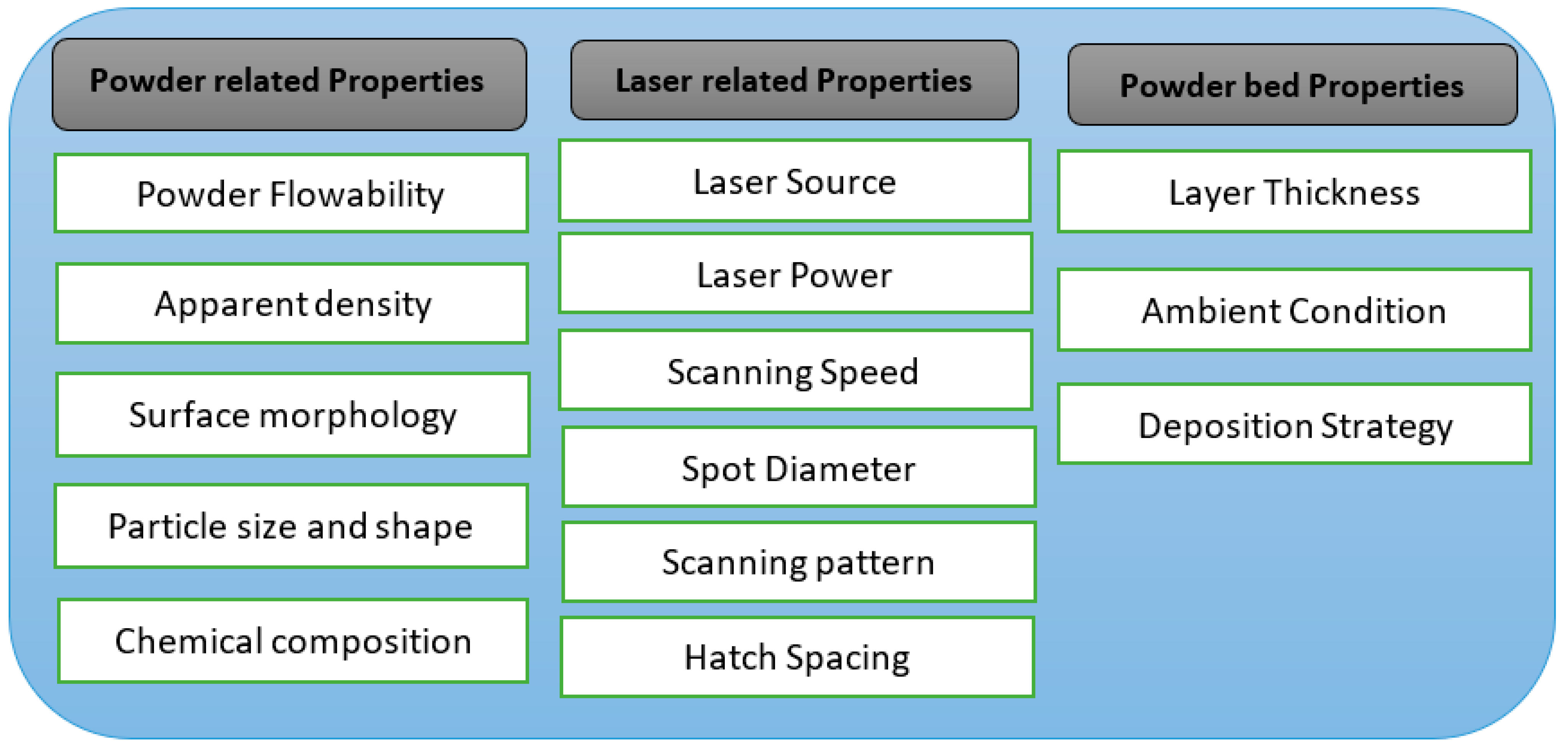
Figure 1. Summary of CW-based SLM process parameters [41].
Qubs 06 00005 g001
Figure 2. Comparison of CW, ns and fs laser material absorption processes [57].
Qubs 06 00005 g002
Figure 3. Energy penetration (red) and volume heated via heat conduction (yellow) or different pulse durations [47].
Qubs 06 00005 g003
Figure 4. Temporal evolution of an fs-laser-based AM process [44]. The inset shows the correlation between pulse number and temperature for different repetition rates.
Qubs 06 00005 g004
Figure 5. Experimental and numerical results of ablation depth as a function of laser fluence using a hydrodynamics model for (a) copper and (b) aluminium with a 170 fs laser pulse (Adapted from reference [119]).
Qubs 06 00005 g005
Figure 6. Schematic of the fs-laser-based selective laser sintering–powder bed fusion process.
Qubs 06 00005 g006
Figure 7. SEM images of Cu line patterns at a constant speed of 0.1 mm/s and laser fluences of (a) 12.8 mJ/cm2 at 195 mW; (c) 13.8 mJ/cm2 at 210 mW where (b,d) are magnified images of regions (A) and (B) (Adapted from reference [52]).
Qubs 06 00005 g007
Figure 8. (a) Spin-coated CuO NP film; femtosecond reductive sintering of (b) electrodes, (c) temperature sensors and (d) non-irradiated parts on the substrate were removed; (e) fs laser reductive sintered line width on PDMS vs. glass as a function of the scanning speed [53].
Qubs 06 00005 g008
Figure 9. SEM images of sintered CuO–NiO NP micropatterns at different scanning speeds: (a) 0.1; (b) 0.5; (c) 1; (d) 3; (e) 5 mm/s [154].
Qubs 06 00005 g009
Figure 10. (a) Schematic of microfabrication of Cu-based patterns within a Cu2O film. Microscopic images of (b) sintered patterns and (c) after Cu2O nanosphere film removal (Adapted from reference [158]).
Qubs 06 00005 g010
Figure 11. (a) The samples fabricated with cuboids of a 2 × 2 mm2 size, and total height of 1.4 mm; (b) SEM images of the sample (Adapted from reference [54]).
Qubs 06 00005 g011
Figure 12. (a) Thin-walled circular samples; (b) SEM image of a single wall (Adapted from reference [54]).
Qubs 06 00005 g012
Figure 13. (a) SEM image of sintered samples, operated at max intensity = 6.74 × 10¹² W/cm2, energy per unit length = 0.7 J/m, scanning speed = 1250 m m/s, line spacing = 10 μm and pulse repetition rate = 125 kHz, 10 scans; (b) SEM image of sintered samples, operated at max intensity = 6.74 × 10¹² W/cm2, energy per unit length = 0.23 J/m, scanning speed = 3750 m m/s, line spacing = 10 μm and pulse repetition rate = 125 kHz, 10 scans; (c) optical image of sintered grid-like structures, operated at max intensity = 1.77 × 10¹² W/cm2, energy per unit length = 3 J/m, scanning speed = 600 m m/s, line spacing = 10 μm, and pulse repetition rate = 1 MHz, 6 scans; (d) SEM image of sintered grid-like structure sample (Adapted from reference [101]).
Qubs 06 00005 g013
Figure 14. Iron rings fabricated by (a) an 80 MHz fs laser; (b) a CW laser (Adapted from reference [7]).
Qubs 06 00005 g014
Figure 15. (a,b) The fs laser 3D printed tungsten cube with fs laser viewed from different angles; (c) polished top surface (Adapted from reference [7]).
Qubs 06 00005 g015
Figure 16. (a) A gear a half-inch in diameter 3D printed by fs laser; (b) fs sintered tungsten feature; (c) fs sintered tungsten with a small circular feature with a hole; (d) 3D printed thin wall of a 100 microns (Adapted from reference [44]).
Qubs 06 00005 g016
Figure 17. Average grain size area as a function of pulse width (Adapted from reference [44]).
Qubs 06 00005 g017
Figure 18. (a) Track width as a function of varying scan speeds with a constant laser power of 100 mW; (b) track width as a function of varying laser powers with a constant scan speed of 0.5 mm/s (Adapted from reference [56]).
Qubs 06 00005 g018
Figure 19. SEM images of fs Ag NPs sintered at various laser fluences (Adapted from reference [173]).
Qubs 06 00005 g019
Figure 20. (a) Neck size; (b) fraction of the exposed area of the PET substrate after fs laser sintering; (c) sheet resistances of the fs laser sintered Ag particles [173].
Qubs 06 00005 g020
Figure 21. Cross-sectional SEM images (a) before fs laser sintering and (b) after fs laser sintering (F = 30 mJ/cm2, effective pulse number = 1000) (Adapted from reference [173]).
Qubs 06 00005 g021
Figure 22. (a) Microstructures of fs sintered Ag particles during surface necking and melting stages. Variations in the resistivity of sintered Ag films as a function of fluence; (b) Np = 1000; (c) Np = 10,000 (Adapted from reference [172]).
Qubs 06 00005 g022
Figure 23. Lithium content versus density and Young’s modulus in Al–Li alloys [60].
Qubs 06 00005 g023
Figure 24. (a) Samples fabricated at different scan velocities (0.2, 0.3, 0.5 and 0.7 m/s, from left to right); Printed structure’s microscopic images with a scan velocity of (b) 0.3 m/s and (c) 0.7 m/s [60].
Qubs 06 00005 g024
Figure 25. (a,b) Figures of a gear wheel fabricated at a scanning speed of 0.7 m/s, pulse energy of 1.5 μJ and 20 MHz pulse repetition rate; (c,d) light microscope images at different locations on the gear [60].
Qubs 06 00005 g025
Figure 26. SEM images of single tracks at different parameters at a pulse energy of 1.25 μJ (Adapted from reference [38]).
Qubs 06 00005 g026
Figure 27. (a) Hollow thin-walled structure fabricated using fs-based AM; (b) hexagonal structure fabricated to a height of 5 mm (Adapted from reference [38]).
Qubs 06 00005 g027
Figure 28. (a) SEM images of the walls (top view) above the parameters and a layer thickness of 15 microns; (b) scan speed versus melt pool width for different lasers; (c) melt pool width at the tip of the wall captured by optical microscopy; (d) scan speed versus aspect ratio between melt pool depth and width (increases for shorter pulse duration) (Adapted from reference [183]).
Qubs 06 00005 g028
Figure 29. (a) SEM images of the tip of wall with a constant scanning speed of 200 mm/s; (b) different pulse durations versus melt pool width; (c) cross-section of two polished walls at 500 fs and 10 MHz repetition rate; (d) different scanning speeds versus aspect ratio [183].
Qubs 06 00005 g029
Figure 30. Schematic of a solid oxide fuel cell.
Qubs 06 00005 g030
Figure 31. (a) Cross-section SEM image of the interface between the functional layer and support layer of an anode; (b) Ni-YSZ anode samples with the cell sample mounted on an Au grid for testing the I-V curve and EIS; (c) sample mounted on grid with Au before testing (d) cell sample after testing (Adapted from reference [191]).
Qubs 06 00005 g031
Table 1. Commercially available laser-based metal AM machines [72].
CategoryManufacturing SystemsLaser
Direct energy deposition (DED)Trumpf GmbH: TruLaser seriesTruDiode diode laser, up to 6 kW (600 nm)
Meltio1200 W diode laser
BeAM: Modulo series500–2000 W fibre laser
Oerlikon Metco Group: MetcoClad systems1–6 kW diode laser
InssTek: Fab seriesMaximum 2000 W fibre laser
Optomec Inc.: LENS series400–1000 W fibre laser
Powder bed fusion (PBF)Renishaw: AM250200 or 400 W fibre laser
SLM Solutions GmbH: SLM systems400–1000 W fibre laser (for metals)
EOS GmbH: EOSINT, EOS M and PRECIOUS M machines30, 70 or 2 × 50 W CO2 lasers (for thermoplastics)
200 W–1 kW fibre laser (for metals)
3D Systems Inc.: ProX, sPro and ProX SLM systems30–200 W CO2 laser (for thermoplastics)
50–500 W fibre laser (for metals)
Concept Laser400–1000 W fibre laser (for metals)
Aconity ONE400–1000 W fibre laser
Trumpf: Truprint 5000500 W fibre laser
Table 2. Laser-based AM and its applications in various fields [73,74].
IndustryTrend/GoalLaser-Based AM Process
Aerospace [12,29]Demand for lightweight structuresDMD, SLS and SLM
Rapid tooling, fixturingDMD and SLS
Fuel reductionDMD, SLS and SLM
Organic featuresSLM, SLS and DMD
Automotive [10]Demand for lightweight structuresSLS, SLM and DMD
Medical (dental, implants) [75]Minimally invasive surgerySMS and SLM
Replication of anatomic structuresSLA and SLS
Biomaterial manufacturingSLS and SLA
Electronics [76]Smart microsystemsSLA and Micro-SLS
MiniaturisationSLA and Micro-SLS
Accelerated product developmentSLA and Micro-SLS
Table 3. Types of lasers and related parameters used in AM processes [77].
Laser TypeCO2 Laser Yb-Fibre LaserNd:YAG LaserExcimer Laser
Type of laserPulsed and CWPulsed and CWPulsed and CWPulsed
AM processSLA, SLM, SLS and LENSSLS, SLM and LENSSLS, SLM and LENSSLA
Wavelength9.4 and 10.6 µm1.07 µm1.06 µm193, 248 and 308 nm
Output power (CW)Up to 20 kWUp to 10 kWUp to 16 kW300 W (average)
Pulse duration100–10 s ns10 s ns to 10 s msFew ns to 10 s ms10 s ns
Efficiency5–20%10–30%10–20%1–4%
Beam quality (mm.mrad)3–50–40.4–200.5–2
Table 4. Different maximum ablation rates for various material processes [96].
MaterialOptimum Avgerage Fluence at 400 fs and 1035 nm (J/cm2)Maximum Ablation Rate at 400 fs and 1035 nm (mm3/W min)
Steel0.350.22
Nitinol0.60.21
Aluminium10.3
Copper1.70.16
Si1.30.16
SiC0.70.13
PET0.78
Fused silica30.4
Sapphire40.3
Table 5. Various factors that influence fs laser material processing [44].
Various FactorsDescription
Pulse energyDepends on the average output power and pulse repetition rate
Pulse widthCalled pulse duration also and, in general, varies a few hundred femtoseconds in the case of fs laser material processing
Average powerTotal average output power utilised in material processing
Pulse repetition rateNumber of pulses per second, in general, between kHz and a few MHz will be utilised during material processing
Peak powerMaximum peak power attained by a single pulse
Focus spot area/volumeThe laser spot area or volume is the exposed area/volume, which is important to consider during precise processing
Hatch spacingThe spacing between each line exposed during area-wise material processing
Scanning velocityThe scan velocity is the speed of the laser travelling during processing; it is the most critical parameter to control because the exposure time depends on this parameter
Operation modeThe environment during processing
WavelengthThe laser operating wavelength
Powder particle sizeThe powder size is important to consider, depending on the application
Shape of the powder particleIn general, for SLS/M spherical powder particles are considered
Powder morphologyThe uniformity of powder size distribution
Table 6. Hardness values for the tungsten sample processed with different lasers [44].
Hardness (HRC)Fs SampleCW Sample20 ps Sample200 ps SampleTungsten Sample
Cross-section47.744.741.845.145.8
Top45.444.944.142.444.9
Table 7. Showing materials processed through femtosecond lasers with different process settings.
Sample NumberMaterialWavelength (nm)Pulse Duration (fs)Pulse Repetition Rate (MHz)Power (W)Scan Speed (mm/s)Spot Diameter (microns)Layer Thickness (microns)Line Spacing (μm)Pulse Energy (J) (or) Fluence (J/cm2) (or) Energy Density (W/cm2)Reference
1Al–40Si10305006–20 MHz252005015 to 30-<0.4 J/cm2[183]
2Al–Li Alloy103050010–20 MHz30100–7003520 to 40-1.5–3 μJ[60]
3AlSi4O (40 microns)103050020 MHz12 to 252005035 to 50-40–170 J/m[38]
4Calcium Phosphate1045130–19010000.40.130--0.4 nJ[62]
5Copper (10 nm)80010080 MHz0.195–0.2100.16.97--12.8–13.8 mJ/cm2[52]
6Copper
(35 microns)
1030 200–20 MHz-833 and 6663530151, 1.25 μJ, 100 J/m[54,138]
7Copper (CuO)78012081 MHz-0.5–20-1000-0.54 nJ[53]
8Cu2O78012083 MHz-1000.7 -163 GW/cm2[158]
9CuO and NiO78012082 MHz-0.1–51.310-0.059 J/cm2[154]
10CuO/Cu2O78012084 MHz-10- -0.74 nJ[152]
11Iron (1–5 microns)103035080 MHz5050- --[7]
12Iron on glass106080080 MHz37 and 53300 and 400-40--[100]
13Monolithic zirconia1030400200 kHz5 ---25 μJ[51]
14Silver (Ag) NP10303701 MHz0.05–0.30.01–5----[56]
15Silver (Ag) NP78010080 MHz0.1–0.40.1–0.6----[174]
16Silver (Ag) NP800501 kHz-0.02–4---10–300 m J/cm2[172]
17Silver (Ag) NP800501 kHz-0.02–0.2--20010–120 m J/cm2[173]
18Silver (Ag) NP7801001 kHz0.5, 0.60.1–0.6----[55]
19SS 316 L793150–2001 kHz0.15-----[46]
20Tungsten10301800.125–1 MHz0.4 to 0.875100–500036-100.4–7.5 μJ, 0.07–1.3 J/cm2[101]
21Tungsten10304001 MHz35202025–50-22.5 μJ[58]
22Tungsten1030750100 kHz to 100 MHzMaximum 1 kW----maximum 500 J[44]
23Tungsten10304001 MHz4525----[7]
24YSZ, Ni-YSZ103080080 MHz130300255–600--[191]
Publisher’s Note: MDPI stays neutral with regard to jurisdictional claims in published maps and institutional affiliations.