Article

Comparative Microstructure Characteristics of Synthesized PbS Nanocrystals and Galena

1
Department of Chemistry, The University of Jordan, Amman 11942, Jordan
2
Department of Physics, The University of Jordan, Amman 11942, Jordan
3
Department of Studies, Research and Development, Ministry of Energy and Infrastructure, Abu Dhabi 11191, United Arab Emirates
4
Department of Scientific Basic Sciences, Faculty of Science, Philadelphia University, Amman 19392, Jordan
5
Department of Geology, The University of Jordan, Amman 11942, Jordan
6
Teacher Training Institute, Emirates School Establishment, Dubai 3962, United Arab Emirates
*
Author to whom correspondence should be addressed.
Sci 2024, 6(4), 61; https://doi.org/10.3390/sci6040061 (registering DOI)
Submission received: 29 July 2024 / Revised: 28 August 2024 / Accepted: 19 September 2024 / Published: 8 October 2024

Abstract

:
Lead sulfide (PbS) on the nanoscale was synthesized via a chemical route at room temperature using lead nitrate {Pb(NO3)2} and sodium sulfide (Na2S). The Na2S was prepared at ~105 °C using sodium hydroxide (NaOH) and sulfur (S) powder. The produced PbS, denoted as Lab-PbS, was compared with a high-concentration PbS phase of galena. The produced Na2S and Lab-PbS were examined using scanning electron microscopy and energy dispersive X-ray spectroscopy for microstructural and chemical analysis. The results confirmed a high-purity PbS compound (>99%) with a nanoscale particle size. The results showed that ultrasonic agitation was vital for obtaining the nanoparticle size of the Lab-PbS. Furthermore, thin films from the synthesized Lab-PbS and galena were successfully thermally evaporated on glass, quartz, and silicon substrates. The formation of nanometric grains was confirmed by scanning electron microscopy (SEM). XRD and FTIR spectroscopy were carried out for the Lab-PbS, galena fine powders, and galena thin films. The average crystal diameter was calculated for the galena thin films and was found to be approximately 26.6 nm. Moreover, the UV–Visible transmission curve was measured for the thin films in the wavelength range of 200–1100 nm in order to calculate the bandgap energy (Eg) for the thin films. The values of Eg were approximately 2.65 eV and 2.85 eV for the galena and Lab-PbS thin films, respectively. Finally, the sintering of the Lab-PbS and galena powders was carried out at ~700 °C for 1 h under vacuum, achieving relative densities of ~98.1% and ~99.2% for the Lab-PbS and galena, respectively.

1. Introduction

The economical production of lead sulfide (PbS) with different particle sizes is imperative for its broad applications in many fields, such as solar cells, infrared detectors, the semiconductor industry, light-emitting diodes, and high-speed switching [1,2,3,4,5,6]. It is possible to control the bandgap energy (Eg) of PbS from a bulk value of about 0.4 eV at room temperature to approximately 5 eV of nanoscale PbS powder for optical sensor fabrication to meet the required specifications and to suit different applications [7,8,9]. PbS nanocrystals have gained special attention due to their advanced technical applications in optical instruments and electronic nano-devices, as the characteristics of this inorganic compound mainly depend on the purity of the starting material, particle size of the used powder, and structural variations that strongly depend on the production methods used. Recently, this subject has been well-reviewed [10]. PbS nano powder produced by mechanochemical synthesis based on PbO and Na2S is an attractive production method [11]. The procedure begins with mechanical milling to obtain a mixture of PbO and Na2S fine powder, and then a stoichiometric quantity of water is added during the milling process to complete the chemical reaction to form nanoscale PbS black powder. PbS powder for different applications can also be produced via the powder metallurgy of high-content PbS phase galena ore. This type of galena can be imported from the United States of America, Nigeria, and Japan, where the mass percentage of lead sulfide in its ores exceeds 98% [12]. This process starts with the selection of suitable galena bulks in conjugation with direct chemical analysis, passing through mechanical milling to obtain powders of different particle sizes down to the nanoscale, followed by powder compaction and sintering to achieve the required specifications and shapes [13].
Many workers in this field have reported different routes for the chemical precipitation of PbS. It was confirmed that the particle size of such products can be controlled by many parameters, such as pH, temperature, reaction time, surfactant solutions, ultrasonic agitation, and mechanical milling [14,15,16,17,18]. Nanoscale PbS was chemically produced using lead nitrate and sodium sulfide compounds with a capping solution to gain unaggregated particles [19]. The main aim was to apply these results for light collection in solar cell applications. The deposition of PbS thin films with nanocrystals on different dielectric substrates by a chemical route has been reported [20]. This study included the effect of the dielectric surfaces of the structure on the produced thin films to select the most appropriate one for transistor fabrication in the form of nanoscale-particle thin films. The microstructure of the deposited PbS thin films was polycrystalline, similar to the cubic galena phase. Hybrid PbS Quantum Dot (QD) thin films with graphene and silicon QDs using a spin coating technique have been reported [21,22]. The results showed that a region of the visible wavelength band that extended to the short infra-red wavelengths could be sensed.
According to the best of our knowledge, no articles have been published on the laboratory synthesis of one compound being used to precipitate PbS in nanoscale powder, such as sodium sulfide (Na2S). Also, no attempt to sinter PbS powder and galena ore powder for comparison purposes has been carried out. Additionally, applying the thermal evaporation technique to produce thin films with nanoscale crystallites, starting with pre-sintered synthesized PbS powder pieces and galena agglomerates to compare their structure and optical properties, has never been addressed.
This research aims to synthesis PbS nano powder using an easy chemical route at room temperature. The project of this research includes the production of a Na2S compound that will be used in synthesizing the PbS powder to reduce production costs. The plan includes investigations of the produced Na2S, synthesized PbS powder, the thermal evaporation of PbS and galena thin films for comparison purposes, and the sintering of PbS and galena powders. Several instruments and tools are used for the sample investigations. Scanning electron microscopes (SEMs), one of which is equipped with an energy-dispersive X-ray analysis (EDS) unit, are employed for microstructure and chemical analysis studies. X-ray diffraction (XRD) is used for phase and crystal size examinations. UV–Visible and Fourier Transform Infrared (FTIR) spectroscopies are conducted to test the obtained PbS and galena powders, as well as the corresponding thin films. The synthesized PbS and galena powders are sintered in a vacuum for a thorough comparison.

2. Experimental Procedure

2.1. Materials

Lead nitrate {Pb(NO3)2}, sodium hydroxide (NaOH) of a 99% purity, and sulfur (S) powder of a 99% purity were used to prepare the Na2S and PbS compounds. All these chemicals were purchased locally. High-content PbS phase galena agglomerates were purchased from the local market in Amman, Jordan. Distilled water, glassware, and ethanol of laboratory grade were used as required. Normal glass slides, quartz slides, and silicon wafer-cuts were used as substrates for the thin films’ thermal evaporation. Figure 1 summarizes the experimental procedure.

2.2. Synthesizing Na2S and PbS Compounds

Pb(NO3)2 was used as a source of lead ions to chemically precipitate the PbS nano powder. Na2S as a reducing compound was produced in the laboratory by reacting NaOH with elemental S powder under controlled conditions. Based on the reaction, 1 mole of NaOH solution reacted with 0.5 mole of S powder to form Na2S.xH2O. The NaOH solution was heated on a hot plate with a magnetic stirrer (HS-3000, S/N 0407-13, Camlab Ltd., Cambridge CB24 5WE, UK) up to approximately 90 °C at first, followed by the gradual addition of S powder under continuous stirring. The color of the solution started to change to form a thick reddish-purple liquid at a temperature of ~95 °C. The temperature continued to increase until it reached ~105 °C. Heating continued until a dry yellow-to-orange solid of Na2S.xH2O was obtained. To obtain anhydrous Na2S, the produced hydrate Na2S.xH2O was heat-treated at ~150 °C for 1 h in a vacuum of about 10−3 Torr [23]. Further heating at ~200 °C in a vacuum for 1 h was performed to achieve better dehydration.
Figure 2 shows the intermediate solution and the 200 °C dried Na2S. The green synthesis of Na2S via the treatment of Na2SO4, by chemical methods and the thermal route of the nonahydrate of Na2S, has been reported in the literature [24,25].
The PbS precipitation process is shown in the following equation:
P b ( N O 3 ) 2 a q + N a 2 S   a q R o o m   T e m p . P b S   ( s ) + 2 N a N O 3 a q
To chemically synthesize the black powder of PbS at room temperature, the following procedure was implemented according to Equation (1):
  • Exactly 1.56 g of Na2S was weighed using a four-digit analytical balance (Model SEJ-205, Taipei, Taiwan) and then dissolved in 200 mL of distilled water to prepare a 0.1 M light-yellow solution. The dissolving process was quite fast at room temperature.
  • A mass of 6.7 g of Pb(NO3)2 was weighed and then dissolved in 200 mL of distilled water on a magnetic stirrer to prepare 0.1 M of a colorless solution.
  • The solution of Na2S was then added to the solution of Pb(NO3)2 under continued stirring for 2 h to achieve a better PbS formation. As soon as the sodium sulfide solution was added to the lead nitrate solution, the PbS black powder began to precipitate. The residual sodium nitrate liquid was removed after the PbS powder settled down.
  • The formed PbS black powder was then washed four times using distilled water followed by washing with methanol once. The washed PbS powder was left to dry at room temperature in a fume hood. The obtained powder was then heated at approximately 105 °C using a vacuum oven (JEIO TECH, MODEL OV-11, AAH13115K, Seoul, Republic of Korea).
  • Another run of PbS precipitation was also conducted, but with ultrasonic agitation using an ultrasonic cleaner (AC ULTRASONIC, 1002. Jeio-Tech Co., Ltd., Seoul, Republic of Korea) at a frequency of 40 kHz to assess the effect of this parameter on the particle size.
  • The precipitation was repeated as required to produce the needed amounts of Na2S and PbS.
  • The produced PbS is denoted as Lab-PbS in the current article. A sample from the Lab-PbS was compacted using a homemade stainless-steel die with a 1.2 cm diameter at a pressure of 350 MPa. The color of the compacted Lab-PbS pellet was similar to that of the PbS enriched-phase galena ore.
It was found that, when the fine Lab-PbS powder was left to dry after washing with alcohol or acetone, it tended to aggregate to form flake-like parts. The produced nano powder formed colloidal-like particles in the washing liquid before drying. This prevented aggregation and, hence, the milling stage. The product could then be used before the final drying for various designed applications. The aggregated black flake-like parts obtained were loose-sintered at 500 °C for 1 h with a heating rate of about 10 °C/min, and they were then furnace-cooled in a vacuum of approximately 10−3 Torr using a tube furnace (Protherm alumina tube furnace, Model PTF 12/50/450, serial No. 0907234, Ankara, Turkey). The thin film thermal evaporation stage required loose-sintered bulk solid pieces. The color changed from black to light grey, which is the same color as galena ore.
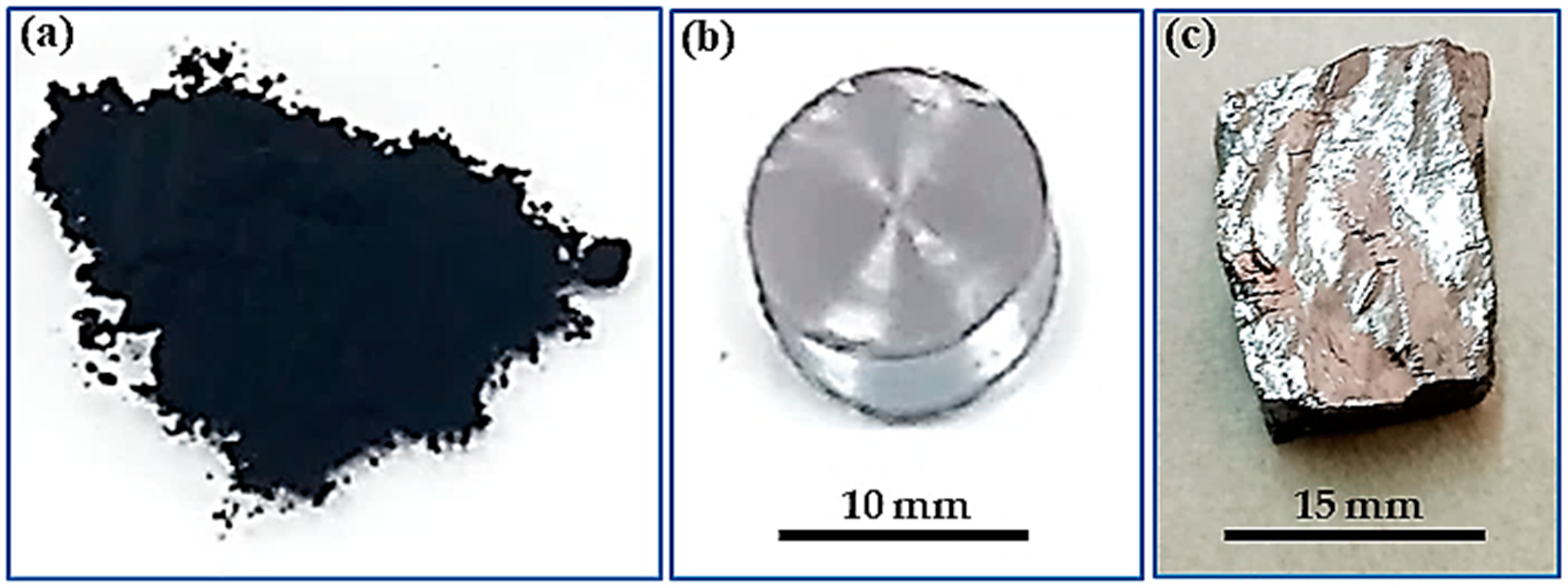
Galena agglomerates of approximately 2 cm in diameter were mechanically crushed using a stainless-steel mortar into small pieces of around 1–3 mm and were then milled for 15 min, using a vibrating milling machine (TEMA, Woodford Halse, UK) to produce an ultra-fine powder. Technical information about this milling machine has been reported [13]. Aggregated pieces of the Lab-PbS powder were also manually fast-milled for 5 min using a ceramic mortar to obtain ultra-fine particles, as it is very brittle and easy to mill. These powders were prepared for XRD and FTIR tests and the sintering stage. Figure 3 shows photos of some milled Lab-PbS, a pellet of compacted Lab-PbS powder, and a sample of galena agglomerates.

2.3. Thin Film Preparation, FTIR, and UV–Visible Spectrophotometry

A thermal evaporation system (SCT-1800, SCT, System Control Technologies, Battle Ground, WA, USA) was used to thermally evaporate the PbS thin films on pre-cleaned glass, silicon, and quartz substrates. Samples of carefully cleaved and cleaned galena and loose-sintered aggregated Lab-PbS were loaded into a tungsten thermal boat. The system was then pumped down to a base pressure of 4.0 × 10⁻⁶ Torr before the evaporation process. The large galena crystals evaporated quickly (~40 s) with a stable evaporation rate of 5 Å/s. The Lab-PbS aggerated particles evaporated almost immediately (~1 s). The prepared samples were measured using UV–Visible spectrophotometry (Shimadzu UV-1601 PC, Shimadzu Scientific Instruments, Columbia, MD, USA) and Fourier Transform Infrared Spectroscopy (FTIR, NEXUS, EPS-87, Thermo Fisher Scientific, Waltham, MA) in the wavenumber range of 400–4000 cm−1. The thickness of the thin films was measured both by the quartz crystal thickness monitor of the evaporation system and by optical reflectance spectroscopy using a FilmTek 3000 (Scientific Computing International, Carlsbad, CA, USA) spectrometer. In addition, the FTIR tests were performed for the two milled powder samples of Lab-PbS and galena. All curves of the four tested samples were graphed and integrated into one figure for direct comparison.

2.4. XRD Measurements for Lab-PbS, Galena, and the Deposited Thin Films

XRD measurements were carried out to identify the phase of the synthesized Lab-PbS (Malvern Panalytical, Aeris, Cu kα1, 1.5406 Å, 0.01 step angle, 2θ ranging from 10° to 90°, Malvern Panalytical, Almelo, The Netherlands). This XRD system was also used to test the galena powder for comparison purposes. The results were analyzed using the software provided with the XRD unit (HighScore Plus version 5.2). The produced thin films with approximate areas of 2 cm2 were also tested by another XRD instrument (Philips PW-1710, 40 kV and 30 mA with a Cu kα tube 1.54178 Å wavelength, 2θ ranging from 10° to 90°, and scan speed of 1 deg/min) to assess and compare their spectra. The Scherrer equation was used for determining the crystallite size of the evaporated galena.

2.5. SEM Product Investigations

The products of the Na2S, Lab-PbS, and galena powders were investigated using SEM coupled with an energy dispersive X-ray analysis (EDS) unit (Thermo Scientific Phenom Desktop SEM, JU-24112022, Waltham, MA, USA). Another SEM (Inspect F50-FEI Company, Eindhoven, The Netherlands) was also used for high-magnification imaging of the Lab-PbS powder and the obtained thin films. All specimens for the SEM investigation were prepared using an aluminum stub with a 1.2 cm diameter, and double-face adhesive carbon tape was used to hold the powder and any other solid specimen. The specimens were coated with platinum thin film using an Agar sputter coater instrument (Agar Scientific, Model AGB7340, Essex, UK) to augment the image quality and to earth the insulator specimens with the stage of the SEM.

2.6. Sintering of Galena and Lab-PbS Powders

The galena ore and Lab-PbS ultra-fine powders were compacted at a pressure of 350 MPa and sintered at 700 °C for 1 h in a vacuum of approximately 10−3 Torr for comparison purposes. The sintering of any compact or loose powder must be carried out under vacuum or under inert gases to avoid oxidation, unless otherwise required. The heating started from room temperature at a rate of 10 °C/min until the sintering temperature was reached, where it was then held for 1 h. Detailed information about milling the galena ore from ultra-fine down to the nanoscale range, compaction, and sintering has been reported recently [13]. The milled aggregate Lab-PbS was compacted and sintered in the same preceding condition. A tube furnace (Protherm alumina tube furnace, Model PTF 12/50/450, serial No. 0907234, Protherm Inc, Ankara, Turkey) with an integrated home-constructed vacuum and argon gas fitting was used in the sintering stage. The density of the galena ore was determined using the water displacement method for comparison purposes with sintered pellets. The green and sintered densities were calculated from dimensions and mass measurements using a digital caliper with a minimum reading of 0.01 mm (Total, TMT 322001, Guangzhou, China) and the analytical balance mentioned in Section 2.2.
SEM was also used to image the sintered samples’ fracture surfaces in order to compare their microstructures. Almost planar fracture surfaces from both sintered pellets were prepared using the same procedure above (Section 2.5) for the SEM test.

3. Results and Discussion

3.1. SEM Investigations of Na2S and Lab-PbS

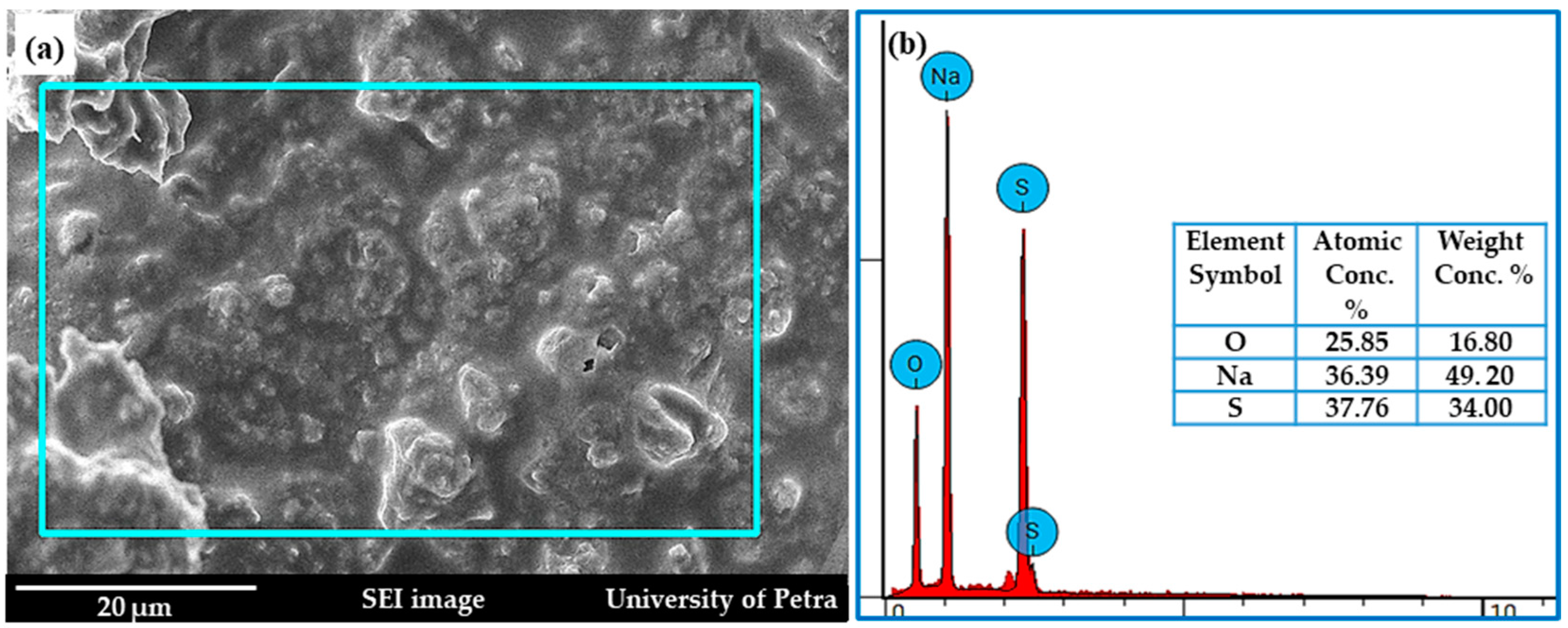
The microstructure and chemical composition of Na2S studied by SEM and EDS are shown in Figure 4. As we will explain next, the results reflect a complete success in producing the required compound according to the procedure used. The presence of an oxygen peak in the spectrum is due to the fact that the Na2S compound is a hygroscopic substance, which can be easily oxidized in air due to the presence of moisture. The reaction with atmospheric moisture is given by:
N a 2 S + H 2 O 2 N a O H + H 2 S
The smell of rotten eggs was noticed when dealing with the produced Na2S during the SEM sample preparation due to the H2S gas formed. The oxygen peak in Figure 4b is due to this reaction, and this is why the mass percentages of Na (49.20%) and S (34.00%) are less compared to those of the pure Na2S, which has mass Na and S element percentages of approximately 59% and 41%, respectively (the Atomic % ratio for Na:S is 2:1).
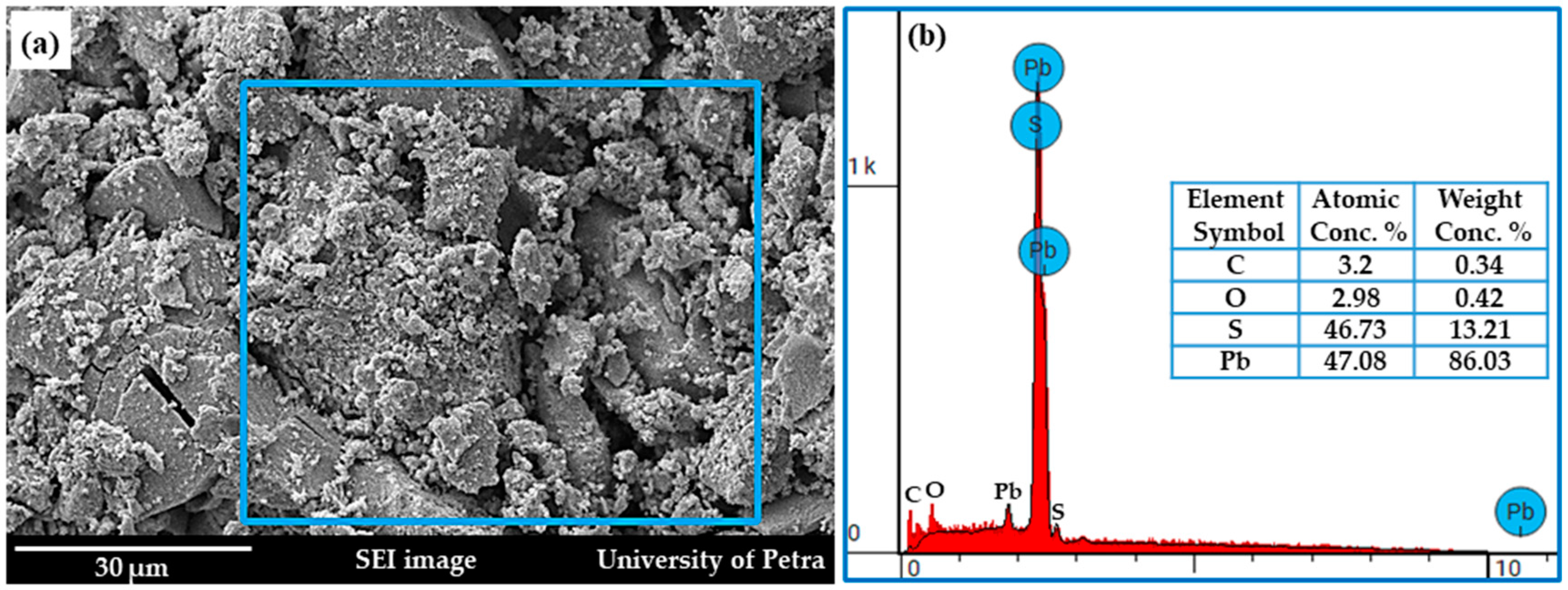
Figure 5 illustrates the morphology of the synthesized Lab-PbS image together with its EDS spectrum and chemical analysis table. The Lab-PbS showed mass percentages of Pb (86.03%) and S (13.21%) similar to the corresponding theoretical values (Pb: 86.6% and S: 13.4%) of this compound (the Atomic % ratio for Pb:S is 1:1). The carbon shown in the elements table is probably due to the carbon tape used to hold the specimen.
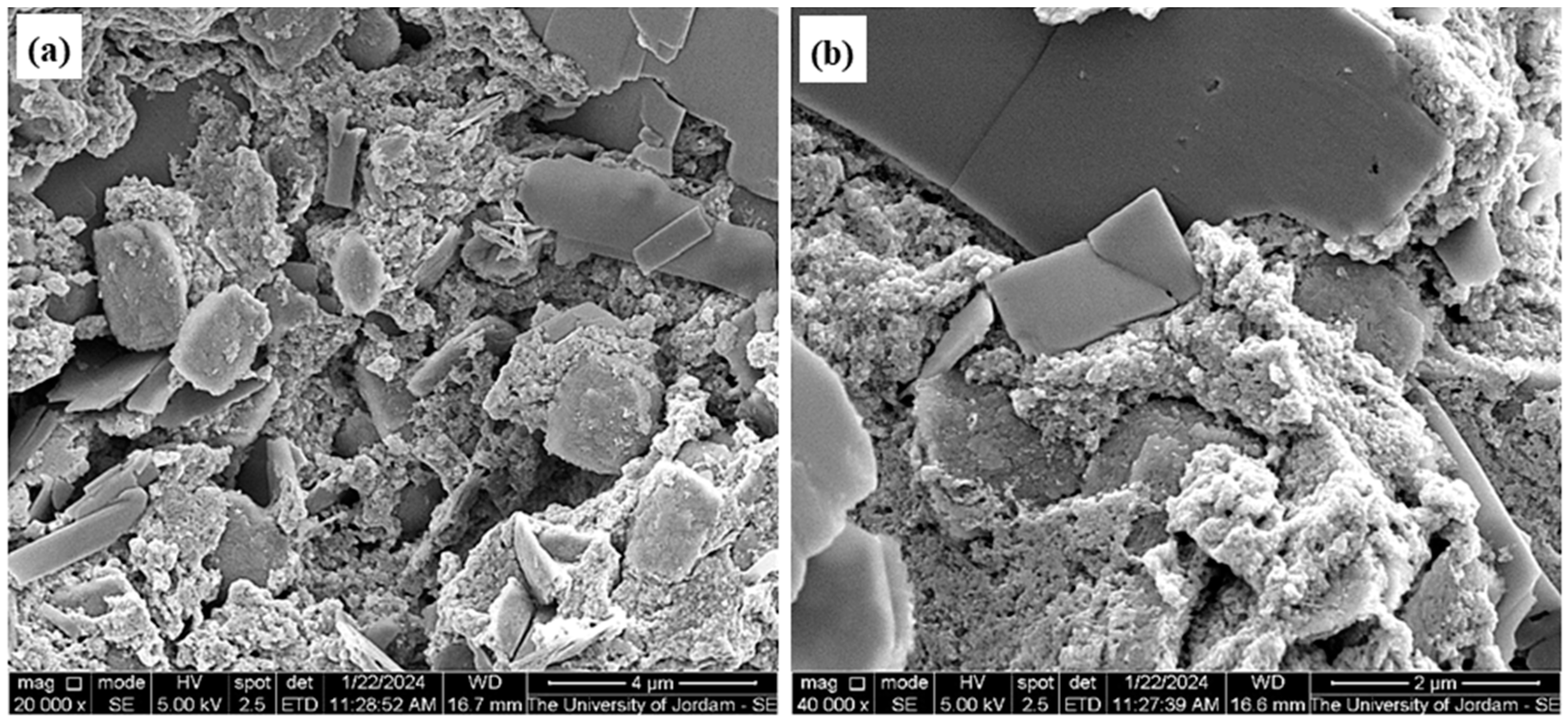
The direct precipitation of Lab-PbS, without applying ultrasonic agitation, quickly settled down, with the particle size being in the microscale range, as shown in Figure 6. The reason for this was probably that the precipitated particles has enough time to aggregate, forming large particles of Lab-PbS.
The synthesized Lab-PbS powder was prepared under ultrasonic agitation during the precipitation process. The morphology and particle size were found to be within the nanoscale range, as revealed by the SEM micrographs in Figure 7. It is clear from the figure that most of the particles are in the nano range, and there are few particles within the size range of 180–320 nm. It seems that ultrasonic agitation is an important factor in preventing aggregation during fine powder nanoscale formation.

3.2. XRD

XRD measurements for the galena and synthesized Lab-PbS powders were carried out for comparison and to check if the phase of the produced lead sulfide was a PbS phase, as shown in Figure 8. The diffractograms are alike and the peaks are completely identical, meaning that the method used to synthesize the PbS powder was successful. Using the software package provided with the XRD system, all peaks of the two diffractograms fit those of the PbS standard and are superposed on each other. This is clear proof that the used galena and produced Lab-PbS were mainly lead sulfide compounds. Table 1 presents the results of the XRD analysis for both the Lab-PbS and galena. The unit cell lattices of the Lab-PbS and galena are within 0.0124% of each other, and both are consistent with the standard XRD of the PbS compound. The lattice unit cell of the Lab-PbS is a bit larger than that of the galena, which perhaps affected the final sintered density, as we will see in the results section.
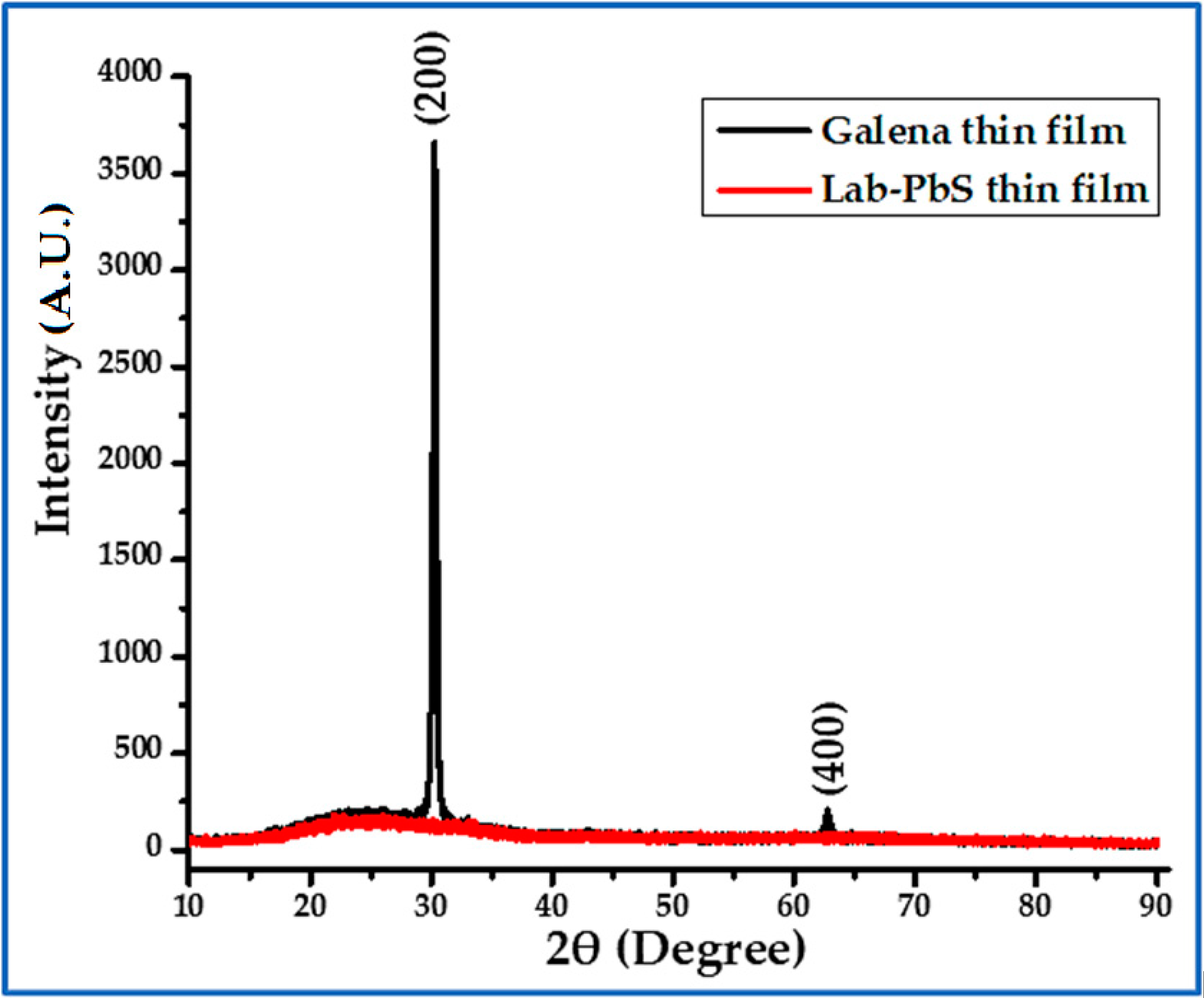
The XRD measurements of the thin films and galena are shown in Figure 9. The diffractograms for both samples are in the 2θ range from 10° to 90°. The figure confirms that there are preferable orientations of crystallization for galena along the (200) plane at 2θ of ~30.3°, as indicated on the figure, and a weak peak for the (400) plane at 2θ of ~62.8°. The thickness of the galena thin film was approximately 150 nm, which was measured by optical reflectance spectroscopy using the FilmTek 3000 (Scientific Computing International, Carlsbad, CA, USA) spectrometer mentioned in Section 2.3. In the case of the Lab-PbS thin film, only the amorphous background spectrum was observed over the whole studied range, and this was probably due to the small thickness of the deposited film for this case, which was about 10 nm. The thickness of the Lab-PbS thin film was significantly smaller than that of the galena. This can be attributed to the fact that the density of the loose-sintered aggregated Lab-PbS was lower than that of the used galena, which led to a very fast evaporation time, ~1 s, for the Lab-PbS case.
The crystallite size for the galena thin film was calculated using the Scherrer’s equation for the two shown peaks in Figure 9. The results showed that the average crystal size was approximately 26.56 nm, which supports the SEM results. The Scherrer’s equation is as follows [26,27]:
D = K   λ β   c o s θ
where D is the average crystallite diameter (nm), K is a constant (equaling 0.94 for spherical crystallites with cubic symmetry), λ is the X-ray wavelength, β is the full width at half maximum (FWHM) of the XRD peak, and θ is the XRD peak angle position. Table 2 includes the galena thin film XRD information, from which the average crystal diameter can be calculated according to Equation (3).
Indeed, the chemical and physical properties of materials produced from powders depend on the particle sizes of their starting substances, purity, and production route parameters. Commonly, materials that are made of crystallites with diameters of 100 nm or less are termed nanomaterials. The main adopted routes for determining the crystal diameter in the nanoscale range are based on electron microscopy. XRD, in conjugation with Scherrer’s equation and Raman spectroscopy, can be also employed in this regard. Recently, accurate crystal size determinations, as well as the techniques used, have been comprehensively reviewed [27].

3.3. Microstructure of Thin Films

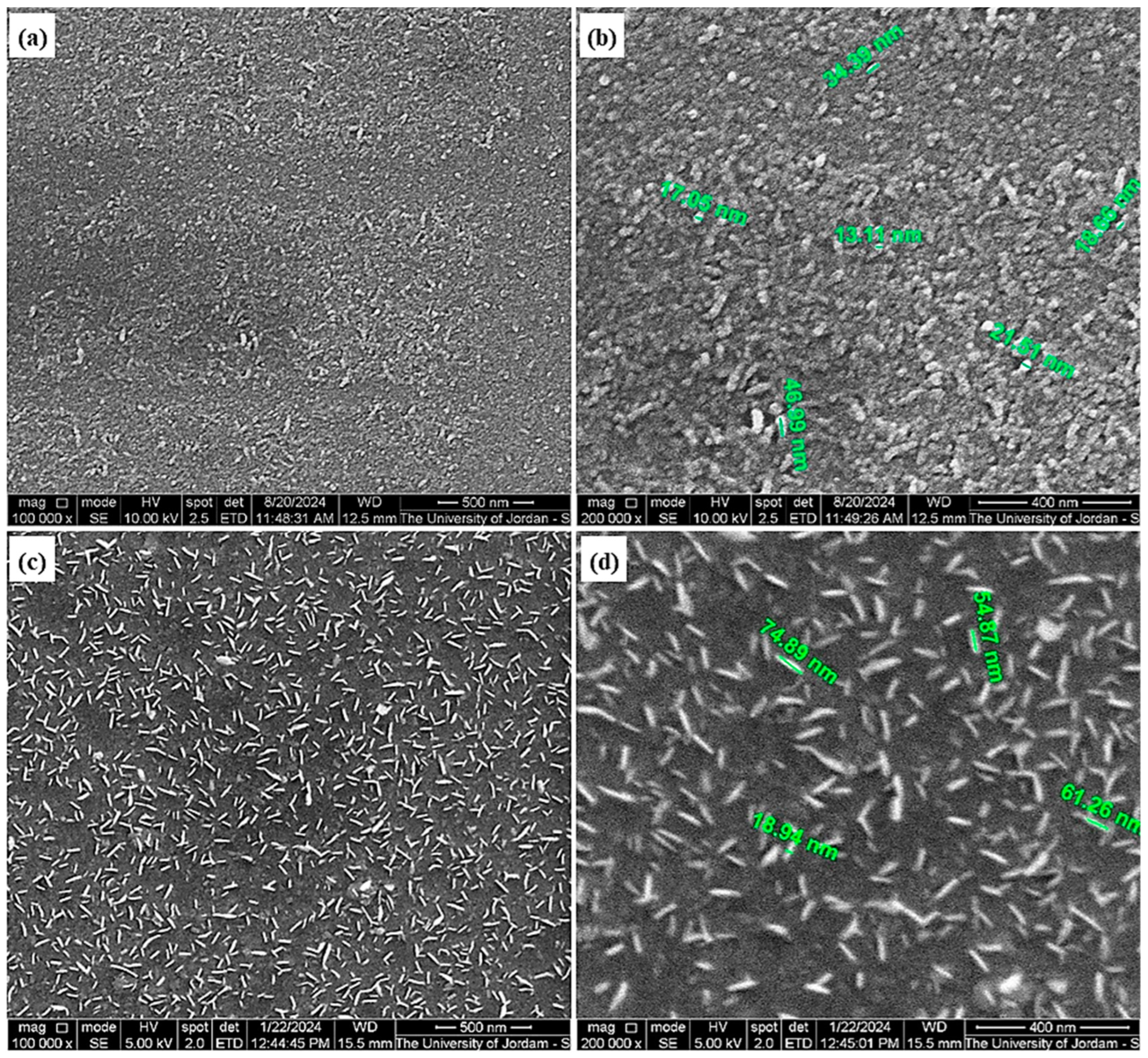
The microstructure of the obtained thin films was investigated using SEM (Inspect F50-FEI Company) at a high magnification and resolution. Figure 10 shows the images of the Lab-PbS and galena thin films with labeled nanoscale measurements.
Both thin films are polycrystalline with a semispherical or rod-like structure, but the particle size of the galena thin film is larger than that of the Lab-PbS thin film, as can be observed in the SEM images. The average particle length of the evaporated galena is ~65 nm, whereas that for the Lab-PbS is ~40 nm. This difference in particle size is probably due to the differences in the properties of the starting materials during the evaporation stage. The galena was fully crystalline bulk pieces, while the Lab-PbS was an aggregated fine PbS powder. This observation is also confirmed by the difference in evaporation time, where it was ~40 s for the galena pieces and ~1 s for the Lab-PbS, as mentioned in Section 2.3, which perhaps led to this variation in the particle size of the evaporated thin films. A point worth mentioning here is that the calculated average particle size of the galena thin film using Scherrer’s formula was 26.56 nm (Section 2.4), which is much less than that estimated from the SEM images above. The reason for this is that Scherrer’s formula was developed for spherical-shaped aggregates, as this was the setting in the used XRD instrument. Therefore, the estimated crystal size from the SEM image differs from that calculated from the XRD data, and that is probably more reliable, since it is seen visually in the SEM micrographs.

3.4. UV–Visible and FTIR Spectroscopy Results

3.4.1. UV–Visible of Thin Films

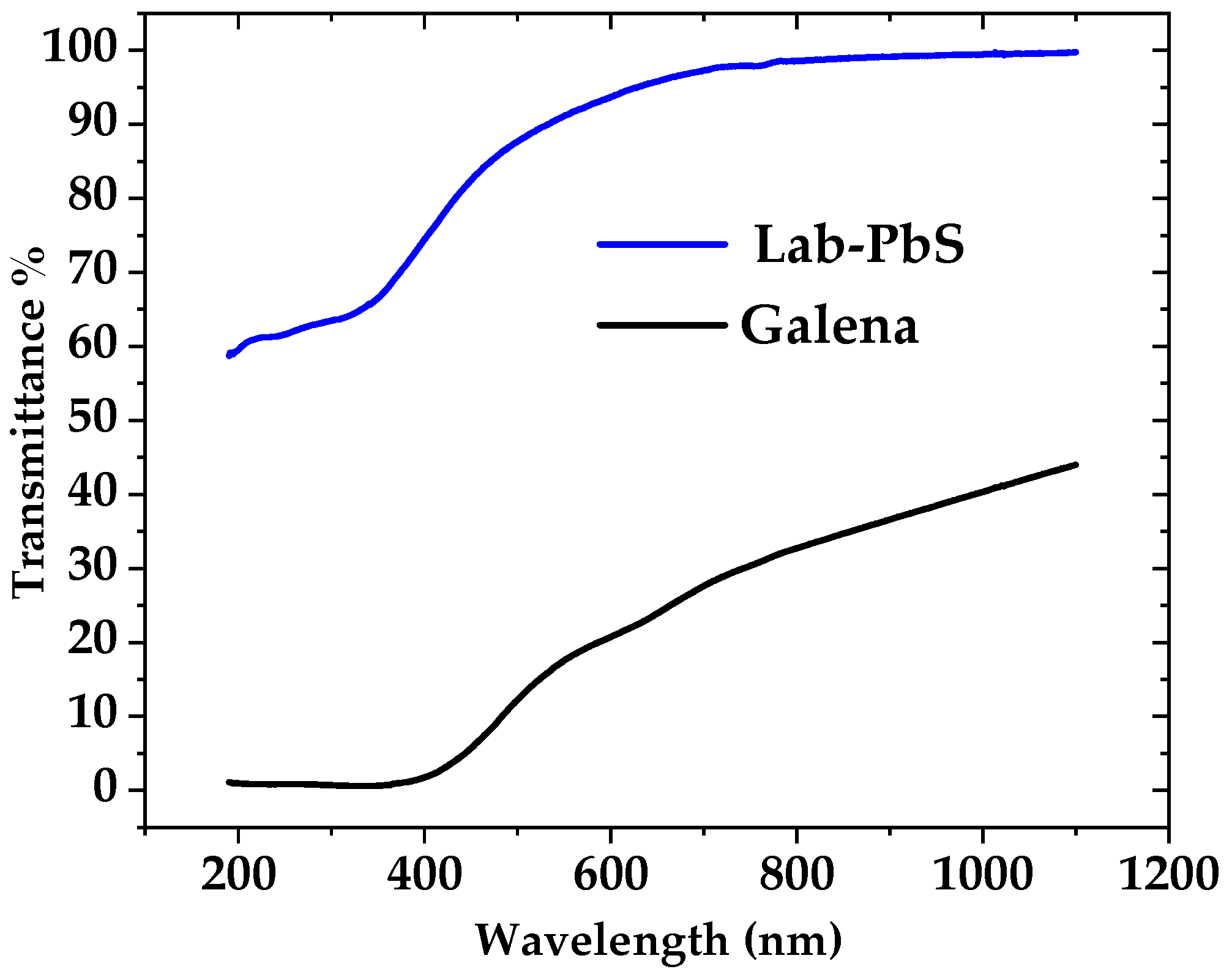
Figure 11 shows the transmission spectra of the as-deposited thin film samples of the Lab-PbS and the galena, which are very similar. The thickness of the galena thin films was ~150 nm, as indicated by the thickness monitor of the evaporation system and as found from optical reflection measurements, while the Lab-PbS sample showed a thickness of ~10 nm. This difference in thickness for the obtained thin films may be attributed to the structural differences of the starting materials. The transmission dependence on the sample’s thickness is easily seen in this figure. The very thin Lab-PbS sample transmittance is almost 60% higher than the corresponding thicker galena thin film across the whole measurement range. Material transmittance behavior is a function of the chemical composition, crystalline structure, and thickness of a material. The thicker galena thin film is better absorbing than the thinner Lab-PbS. The general profile of both films is consistent, with the absorption edge being at almost the same wavelength. Both thin films absorb in the UV region below a 400 nm wavelength.
The higher radiation absorption is also obvious for the thicker galena thin films. One of the attractive features of PbS thin films is their absorption and interaction with IR radiation, as can be easily seen in this figure (the IR range is 780 nm and above).
The Tauc method was used to determine the bandgap energy (Eg) for the deposited thin films. The PbS bandgap has been reported as a direct Eg that depends on the film thickness and crystallite size of the PbS [26]. In this method, a graph of (αhν)2 versus hν is drawn, and the linear region can either be linearly fitted or extrapolated to obtain the corresponding direct Eg. In this work, the linear region was linearly fitted, as seen in the insets in Figure 12, to achieve a higher accuracy of the Eg value and to estimate the corresponding error in the calculated values. Figure 13 illustrates the details of these calculations. The Eg for the thicker film evaporated from galena was 2.647 ± 0.012 eV, while the thinner film evaporated from the Lab-PbS showed an Eg value of 2.845 ± 0.013 eV. These values are consistent with values reported in the literature [28,29,30,31].

3.4.2. FTIR Analysis

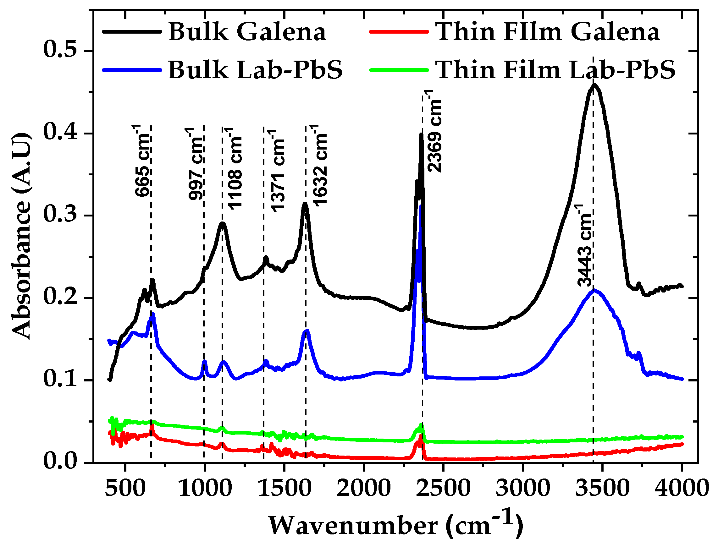
The FTIR absorption spectra for the galena powder, Lab-PbS powder, and thin films of PbS samples deposited on silicon from both sources are shown in Figure 13. A comparison of the finger-print regions of these samples (below 1500 cm−1) shows many common peaks between the bulk and thin film samples. The differences noticed in the intensity between the bulk and thin film samples were expected due to their different thicknesses and bond concentrations. The peaks at around 665 cm−1 are attributed to PbO vibrations, while that at ~997 cm−1 can be assigned to PbS2O3. The peak at 1108 cm−1 can also be attributed to symmetric SO3 vibration in bulk PbSO3, while the peak at 1632 cm−1 is usually assigned to H-O-H deformation. The band at around 2369 cm−1 is due to antisymmetric CO2 stretching and the band at around 3443 cm−1 is due to the stretching modes of water molecules on the bulk galena and Lab-PbS surfaces. The FTIR data suggest the thermal evaporation method as a possible technique to deposit good-quality PbS thin films for different applications [32,33,34,35,36,37,38,39].

3.5. Sintering Investigation

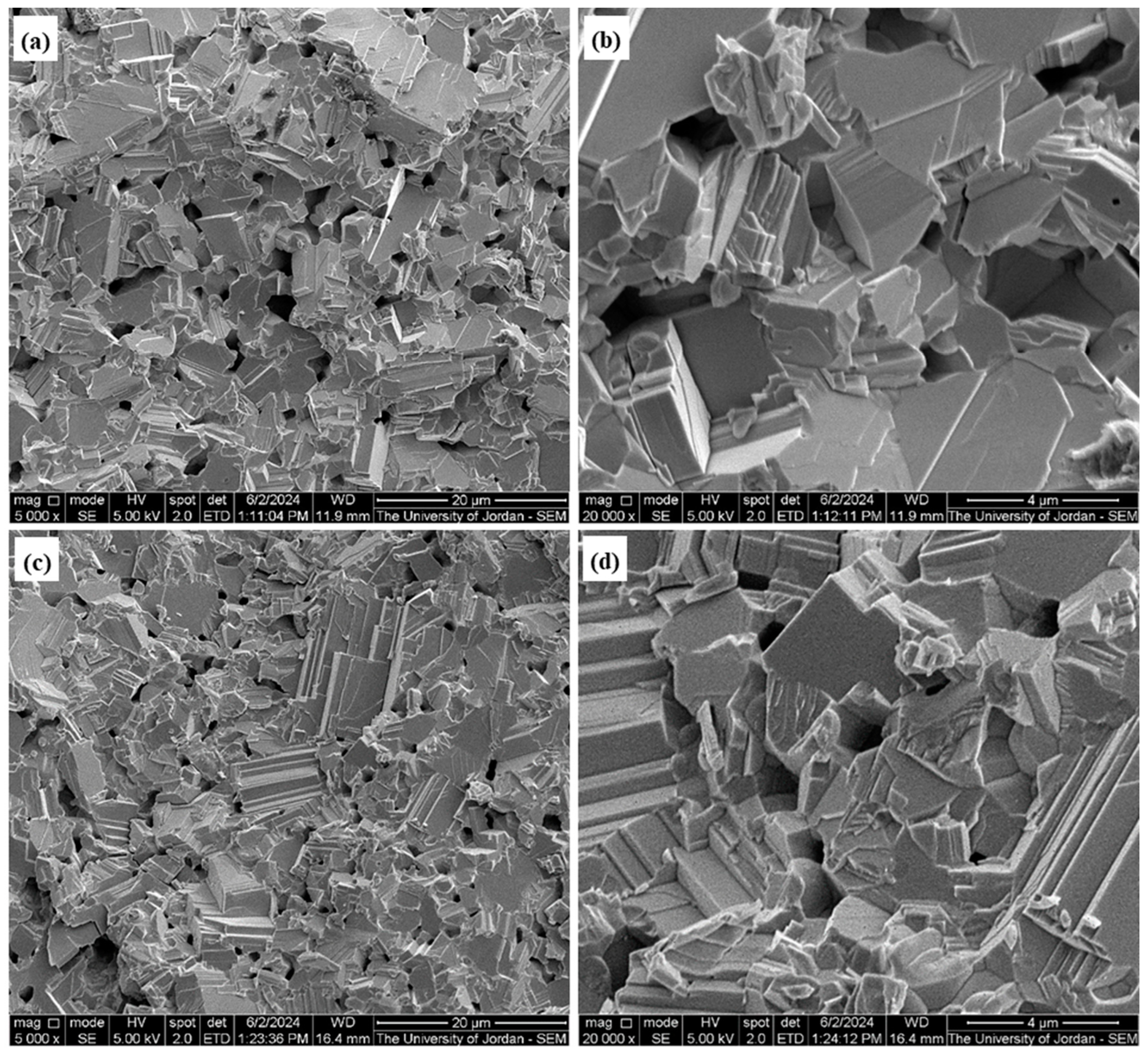
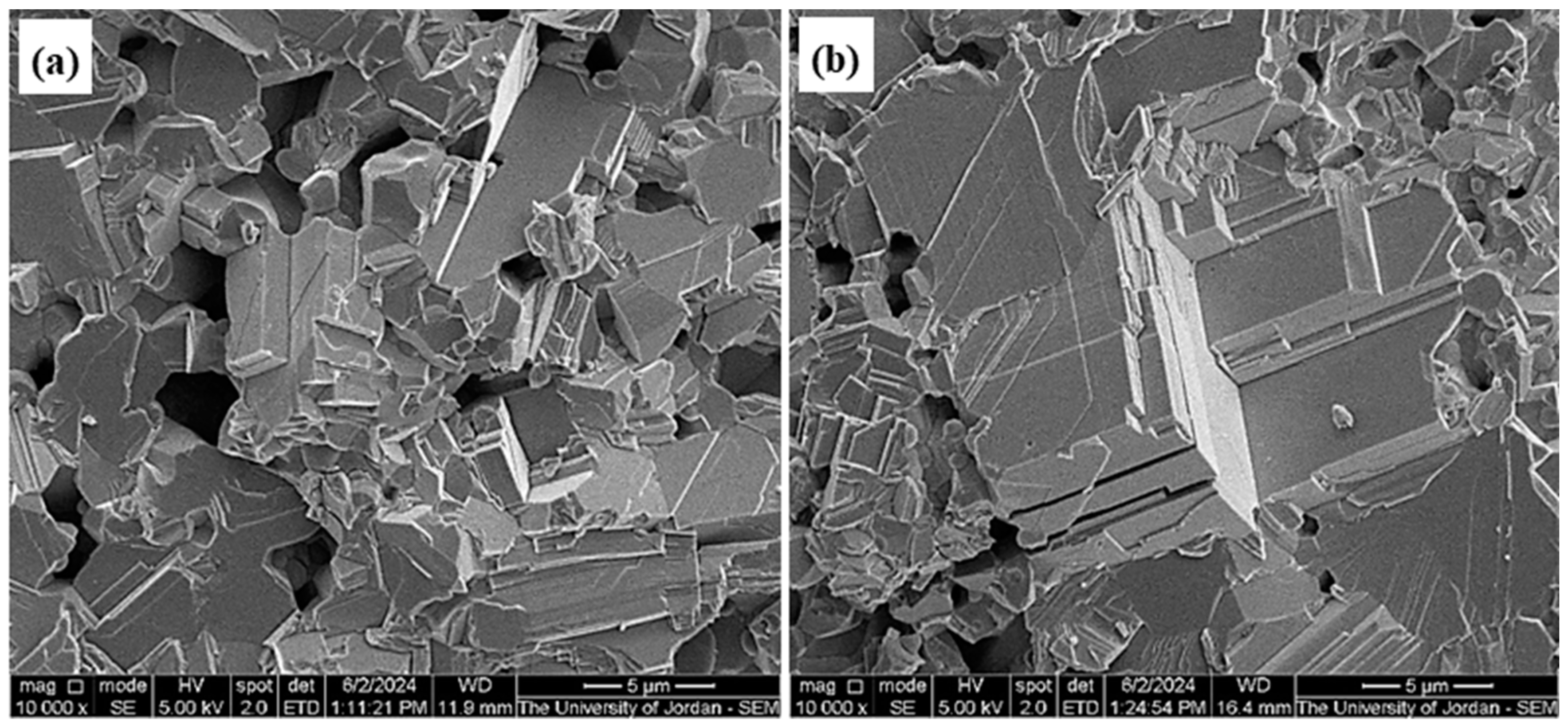
The microstructures of the sintered galena and Lab-PbS powders showed similar cleavage features of their fracture surfaces, as shown in Figure 14, with two unified magnifications for easier comparison (a and c at 5000× and b and d at 20,000×). Both samples show perfect right-angle fracture topography, which is similar to the fracture cleavage of the galena ore [13]. The difference between the two cases is that the pore size in the sintered Lab-PbS is smaller than that of the galena one, and the grain size is a bit smaller, as slightly distinguished. Figure 15 exposes other SEM imaging regions to confirm the similarity in the microstructures of the sintered samples. Extensive information about compaction, sintering at different temperatures, and microstructure was recently reported by Al-Saqarat et al. [40]. This subject needs more work for extra information about the effects of microstructure under different conditions of compaction and sintering on the final product properties.
Table 3 includes details about the compaction and sintering processes, with the green and sintered densities of the two cases. The average relative sintered density (RD%) of Lab-PbS was slightly lower than that of galena according to the mentioned sintering conditions in the table (~1%). The reason for this result is probably due to the fact that the lattice unit cell of the Lab-PbS was a bit larger than that of the galena (Section 3.2). The density of galena ore was found to be approximately 7.42 g/cm3, as determined by the water displacement method (Section 2.6). The RD% is the ratio of the sintered density to the density of galena, which was already determined in Section 2.6, multiplied by 100. This result is encouraging for the production of bulk pieces for large-scale applications using the powder metallurgy route. Powder production mostly ends with compaction and sintering to produce the parts required for scientific and practical applications after determining the suitable sintering conditions to achieve the desired goal.
Finally, PbS nanoparticle powder can be synthesized chemically at room temperature, while the reductant Na2S compound can be prepared in the laboratory starting from NaOH and S powder. Thin films from synthesized Lab-PbS and galena agglomerates can be produced by the thermal evaporation. The produced powder can be sintered under vacuum at approximately 700 °C to find the required size for different applications using the powder metallurgy route. The parameters of sintering are easily controllable, such as the shape, starting particle size, compaction pressure, sintering temperature and atmosphere, martial doping, and rates of heating and cooling. The sintered parts of Lab-PbS and galena agglomerates can be broken into small pieces prior to thermal evaporation for thin film fabrication.

4. Conclusions

The novelty of this research is its success in synthesizing nanoscale PbS compounds at room temperature and productizing the reductant substance of Na2S in the laboratory. This will inevitably lead to a decrease in production costs, as well as improving the production process. The Lab-PbS and galena were thermally evaporated under high vacuum to obtain thin films, where their optical properties were studied. Their morphology and particle size were different (semispherical or rod-like). The bandgap energies of the Lab-PbS and galena were ~2.85 eV and ~2.65 eV, respectively. High-concentration PbS phase galena was used to fabricate crystalline thin films similar to that prepared from the Lab-PbS powder. Scanning electron microscopy was used to study the microscopic structure and chemical composition of the products and the as-received galena. XRD, FTIR, and UV–Visible techniques were used for phase, chemical, and physical investigations of the Lab-PbS and galena powders and for the evaporated thin films. The phases of both were the same (cubic). High RDs% of approximately 99.2% and 98.1% were successfully achieved for the galena and Lab-PbS, respectively, employing powder metallurgy.
Overall, PbS powder can be chemically synthesized at room temperature in the nanoscale range. The powder can be sintered under vacuum at 700 °C, producing various sizes and shapes for different applications. Moreover, pieces from loose-sintered Lab-PbS and galena can be used for the thermal thin film evaporation.

Author Contributions

Conceptualization, E.A.; data curation, B.L., W.M. and I.S.M.; formal analysis, B.L., W.M. and I.S.M.; funding acquisition, E.A., A.N.A.-M., M.A.-Q. and M.A.; investigation, A.N.A.-M., M.A.-Q., M.A. and I.S.M.; methodology, B.L., M.A.-Q. and I.S.M.; project administration, E.A.; resources, E.A., A.N.A.-M. and M.A.; software, M.A.; supervision, E.A. and I.S.M.; validation, B.L., M.A.-Q., W.M. and I.S.M.; visualization, B.L. and I.S.M.; writing—original draft, E.A., B.L., A.N.A.-M., M.A.-Q., W.M., M.A. and I.S.M.; writing—review and editing, E.A., B.L. and I.S.M. All authors have read and agreed to the published version of the manuscript.

Funding

This research received no external funding.

Institutional Review Board Statement

Not applicable.

Informed Consent Statement

Not applicable.

Data Availability Statement

The original contributions presented in the study are included in the article. Further inquiries can be directed to the corresponding author.

Acknowledgments

The authors highly thank Abeer Malhis from the department of chemistry at the University of Jordan for helping in the FTIR measurements. Thanks are extended to Yousuf Abu-Salha from the department of geology and Imad Hamadneh from the department of chemistry at the University of Jordan for their kind help in performing the XRD tests. The authors also thank the chemistry department at the University of Petra for using their SEM with its EDS unit to do the chemical analysis for some samples.

Conflicts of Interest

The authors declare no conflict of interest.

References

  1. Zheng, S.; Chen, J.; Johansson, E.M.J.; Zhang, X. PbS Colloidal Quantum Dot Inks for Infrared Solar Cells. iScience 2020, 23, 101753. [Google Scholar] [CrossRef] [PubMed]
  2. Mishra, A.K.; Saha, S. Fabrication and comparison of photovoltaic devices based on different shape PbS nanoparticles. Mater. Res. Express 2021, 8, 015020. [Google Scholar] [CrossRef]
  3. Sukharevska, N.; Bederak, D.; Goossens, V.M.; Momand, J.; Duim, H.; Dirin, D.N.; Kovalenko, M.V.; Kooi, B.J.; Loi, M.A. Scalable PbS Quantum Dot Solar Cell Production by Blade Coating from Stable Inks. ACS Appl. Mater. Interfaces 2021, 13, 5195–5207. [Google Scholar] [CrossRef] [PubMed]
  4. Islam, M.A.; Sarkar, D.K.; Shahinuzzaman, M.; Wahab, Y.A.; Khandaker, M.U.; Tamam, N.; Sulieman, A.; Amin, N.; Akhtaruzzaman, M. Green Synthesis of Lead Sulphide Nanoparticles for High-Efficiency Perovskite Solar Cell Applications. Nanomaterials 2022, 12, 1933. [Google Scholar] [CrossRef]
  5. Mukai, K.; Masuda, I. Theoretical study of multi-band solar cells with a single PbS quantum dot superlattice film as a light absorption layer. Jpn. J. Appl. Phys. 2022, 61, 102005. [Google Scholar] [CrossRef]
  6. Mukai, K.; Ikeda, S.; Pribyl, I.; Sato, H.; Masuda, I. Improvement of solar cell performance using PbS quantum dot superlattices with iodine ligands. Colloids Surf. A Physicochem. Eng. Asp. 2024, 685, 133285. [Google Scholar] [CrossRef]
  7. Mamiyev, Z.Q.; Balayeva, N.O. Preparation and optical studies of PbS nanoparticles. Opt. Mater. 2015, 46, 522–525. [Google Scholar] [CrossRef]
  8. Mishra, A.K.; Saha, S. Synthesis and Characterization of PbS Nanostructures to Compare with Bulk. Chalcogenide Lett. 2020, 17, 147–159. Available online: https://chalcogen.ro/147_MishraAK.pdf (accessed on 1 June 2024). [CrossRef]
  9. Reddy, T.S.; Krishna, S.V.; Kumar, A.V.; Ramanjaneyulu, M.; Sekhar, N.R.; Kumar, M.C.S. Facile synthesis and characterization of PbS thin films doped with various aluminum concentrations for photovoltaic applications. Semicond. Sci. Technol. 2024, 39, 075018. [Google Scholar] [CrossRef]
  10. Mamiyev, Z.; Balayeva, N.O. PbS nanostructures: A review of recent advances. Mater. Today Sustain. 2023, 21, 100305. [Google Scholar] [CrossRef]
  11. Meng, W.; Yuan, W.; Wua, Z.; Wang, X.; Xu, W.; Wang, L.; Zhang, Q.; Zhang, C.; Wang, J.; Song, Q. Mechanochemical synthesis of lead sulfide (PbS) nanocrystals from lead oxide. Powder Technol. 2019, 347, 130–135. [Google Scholar] [CrossRef]
  12. Nnanwube, I.A.; Onukwuli, O.D. Hydrometallurgical Processing of a Nigerian Galena Ore in Nitric Acid: Characterization and Dissolution Kinetics. J. Miner. Mater. Charact. Eng. 2018, 6, 271–293. [Google Scholar] [CrossRef]
  13. Al-Saqarat, B.S.; Al-Mobydeen, A.; AL-Masri, A.N.; Esaifan, M.; Hamadneh, I.; Moosa, I.S.; AlShamaileh, E. Facile Production Method of PbS Nanoparticles via Mechanical Milling of Galena Ore. Micromachines 2023, 14, 564. [Google Scholar] [CrossRef] [PubMed]
  14. Kozhevnikova, N.S.; Uritskaya, A.A.; Rempel, A.A. Dependence of the size of nanoparticles of lead sulfide PbS on the chemical affinity of its formation reaction. Dokl. Phys. Chem. 2013, 453, 270–273. [Google Scholar] [CrossRef]
  15. Tshemese, Z.; Khan, M.D.; Mlowe, S.; Revaprasadu, N. Synthesis and characterization of PbS nanoparticles in an ionic liquid using single and dual source precursors. Mater. Sci. Eng. B 2018, 227, 116–121. [Google Scholar] [CrossRef]
  16. Patel, J.D.; Mighri, F.; Ajji, A.; Chaudhuri, T.K. Morphology and size control of lead sulphide nanoparticles produced using methanolic lead acetate trihydrate–thiourea complex via different precipitation techniques. Martials Chem. Phys. 2012, 132, 747–755. [Google Scholar] [CrossRef]
  17. Chatterjee, B.; Bandyopadhya, A. Characterization of PbS nanoparticles synthesized using sodium lauryl sulfate at room temperature. Mater. Today Proc. 2023, 76, 114–119. [Google Scholar] [CrossRef]
  18. Baláž1, P.; Pourghahramani, P.; Dutková, E.; Fabián, M.; Kováč, J.; Šatka, A. PbS nanostructures synthesized via surfactant assisted mechanochemical route. Cent. Eur. J. Chem. 2009, 7, 215–221. [Google Scholar] [CrossRef]
  19. Jyothilakshmi, V.P.; Bhabhina, N.M.; Dharsana, M.V.; Swaminathan, S. Wet chemical synthesis of lead sulfide nanoparticles and its application as light harvester in photovoltaic cell. Mater. Today Proc. 2020, 33, 2125–2129. [Google Scholar] [CrossRef]
  20. Sanchez-Martinez, A.; Ceballos-Sanchez, O.; Guzmán-Caballero, D.E.; Avila-Avendano, J.A.; Pérez-García, C.E.; Quevedo-López, M.A.; Ramírez Bon, R. Morphological, structural, and electrical properties of PbS thin films deposited on HfO2, SiO2, and Al2O3 for TFTs applications. Ceram. Int. 2021, 47, 18898–18904. [Google Scholar] [CrossRef]
  21. Zheng, L.; Zhou, W.; Ning, Z.; Wang, G.; Cheng, X.; Hu, W.; Zhou, W.; Liu, Z.; Yang, S.; Xu, K.; et al. Ambipolar Graphene–Quantum Dot Phototransistors with CMOS Compatibility. Adv. Opt. Mater. 2018, 6, 1800985. [Google Scholar] [CrossRef]
  22. Zhou, W.; Zheng, L.; Ning, Z.; Cheng, Y.; Wang, F.; Xu, K.; Xu, R.; Liu, Z.; Luo, M.; Hu, W.; et al. Silicon: Quantum dot photovoltage triodes. Nat. Commun. 2021, 12, 6696. [Google Scholar] [CrossRef] [PubMed]
  23. McAuliffe, R.D.; Petrova, V.; McDermott, M.J.; Tyler, J.L.; Self, E.C.; Persson, K.A.; Liu, P.; Veith, G.M. Synthesis of model sodium sulfide films. J. Vac. Sci. Technol. A 2021, 39, 053404. [Google Scholar] [CrossRef]
  24. Roelands, M.; Cuypers, R.; Kruit, K.D.; Oversloot, H.; de Jong, A.; Duvalois, W.; van Vliet, L.; Hoegaerts, C. Preparation & characterization of sodium sulfide hydrates for application in thermochemical storage systems. Energy Procedia 2015, 70, 257–266. [Google Scholar] [CrossRef]
  25. Du, Z.; Liu, F.; Liu, J.; Pan, F.; Fan, C.; Zhang, J. A green process for producing Na2S from waste Na2SO4 through hydrogen agglomerate fluidized bed reduction of BaSO4. J. Clean. Prod. 2022, 355, 131816. [Google Scholar] [CrossRef]
  26. Amir Hussain, M.; Rajen Singh, L.; Ranibala Devi, S. Studies ON Structural, Optical and Electrical Properties of Zn-Doped PbS Nanocrystalline Thin Film. Chalcogenide Lett. 2021, 18, 103–111. [Google Scholar] [CrossRef]
  27. Hassanzadeh-Tabrizi, S.A. Precise calculation of crystallite size of nanomaterials: A review. J. Alloys Compd. 2023, 969, 171914. [Google Scholar] [CrossRef]
  28. Akhtar, S.; Saeed, N.; Hanif, M.B.; Rehman, Z.; Dogar, S.; Mahmood, W.; Mosiałek, M.; Napruszewska, B.D.; Motola, M.A.M.; Khan, A.F. PbS and PbO Thin Films via E-Beam Evaporation: Morphology, Structure, and Electrical Properties. Materials 2022, 15, 6884. [Google Scholar] [CrossRef]
  29. Sahadevan, J.; Muthu, S.E.; Kulathuraan, K.; Arumugam, S.; Kim, I.; Sri Pratha, G.B.; Sivaprakash, P. Structural, morphology and optical properties of PbS (Lead Sulfide) thin film. Mater. Today Proc. 2022, 64, 1849–1853. [Google Scholar] [CrossRef]
  30. Rajathi, S.; Kirubavathi, K.; Selvaraju, K. Preparation of nanocrystalline Cd-doped PbS thin films and their structural and optical properties. J. Taibah Univ. Sci. 2017, 11, 1296–1305. [Google Scholar] [CrossRef]
  31. Zaragoza-Palacios, B.G.; Torres-Duarte, A.R.; Castillo, S.J. Synthesis and characterization of nanoparticles and thin films of PbS by a high-performance procedure using CBD. J. Mater. Sci. Mater. Electron. 2021, 32, 22205–22213. [Google Scholar] [CrossRef]
  32. Donato, D.P.; Cases, J.M.; Kongolo, M.; Michot, L.; Burneau, A. Infrared Investigation of amylxanthate Adsorption on Galena: Influence of oxidation, pH, and Grinding. Colloids Surf. 1990, 44, 207–228. [Google Scholar] [CrossRef]
  33. Chernyshova, I.V. An in situ FTIR study of galena and pyrite oxidation in aqueous solution. J. Electroanal. Chem. 2003, 558, 83–98. [Google Scholar] [CrossRef]
  34. Nabiyouni, G.; Moghimi, E.; Hedayati, K.; Jalajerdi, R. Room temperature synthesis of lead sulfide nanoparticles. Main Group Met. Chem. 2012, 35, 173–178. [Google Scholar] [CrossRef]
  35. Mohamed, W.S.; Ali, H.M.; Adam, A.G.; Shokr, E.K. Vacuum-evaporated PbS:0.03 Zn thin films with varying thicknesses for environmental applications. Opt. Mater. 2024, 148, 114885. [Google Scholar] [CrossRef]
  36. Chirita, P. Galena Oxidation in Oxygen-Bearing Acidic Solutions. ACS Earth Space Chem. 2019, 3, 2593–2600. [Google Scholar] [CrossRef]
  37. Jameel, M.H.; Saleem, S.; Hashim, M.; Roslan, M.S.; Somaily, H.H.N.; Hessen, M.M.; El-Bahy, Z.M.; Ashiq, M.G.B.; Hamzah, M.Q.; Jabbar, A.H.; et al. A comparative study on characterizations and synthesis of pure lead sulfide (PbS) and Ag-doped PbS for photovoltaic applications. Nanotechnol. Rev. 2021, 10, 1484–1492. [Google Scholar] [CrossRef]
  38. Rosly, N.Z.; Abdullah, A.H.; Kamarudin, M.A.; Ashari, S.E.; Ahmad, S.A.A. Adsorption of Methylene Blue Dye by Calix [6] Arene-Modified Lead Sulphide (Pbs): Optimisation Using Response Surface Methodology. Int. J. Environ. Res. Public Health 2021, 18, 397. [Google Scholar] [CrossRef]
  39. Yepseu, P.Y.; Girardet, T.; Nyamen, L.D.; Fleutot, S.; Ketchemen, K.I.Y.; Kun, W.N.; Cleymand, F.; Ndifon, P.T. Synthesis and Photocatalytic Activity of High-Quality Lead (II) Sulfide Nanoparticles from Lead (II) Thiosemicarbazone Complexes as Single Source Precursors. J. Nanomater. 2024, 2024, 9932000. [Google Scholar] [CrossRef]
  40. Al-Saqarat, B.S.; Al-Mobydeen, A.; Al-Dalahmeh, Y.; AL-Masri, A.N.; Altwaiq, A.M.; Hamadneh, I.; Abu-Afifeh, Q.; Zoubi, M.M.; Esaifan, M.; Moosa, I.S.; et al. Study of Galena Ore Powder Sintering and Its Microstructure. Metals 2024, 14, 439. [Google Scholar] [CrossRef]
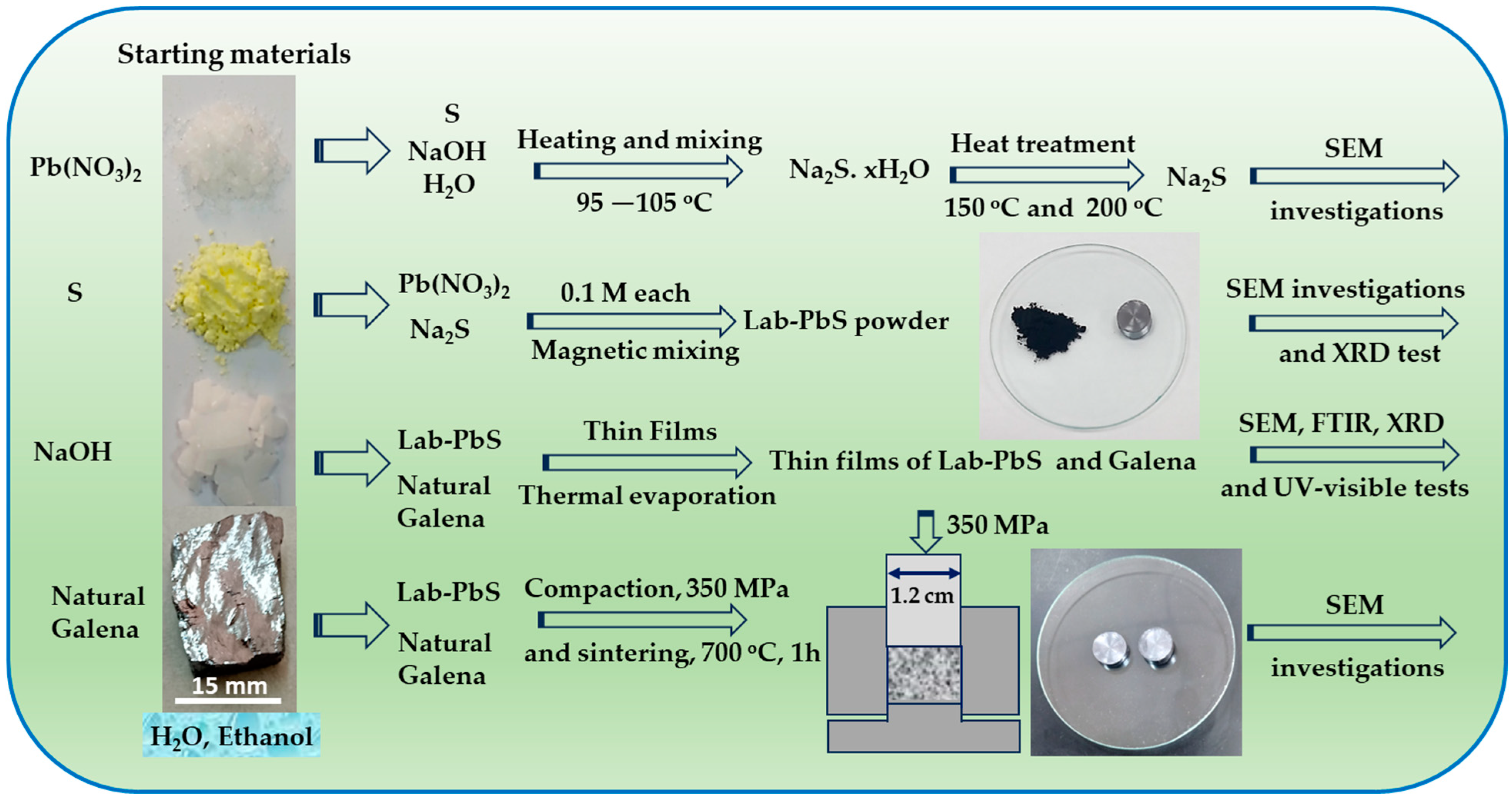
Figure 1. Research implementation procedure.
Sci 06 00061 g001
Figure 2. The intermediate solution of Na2S (left) and the dried Na2S at 200 °C under vacuum (right).
Sci 06 00061 g002
Figure 3. (a) Milled Lab-PbS powder, (b) compacted pellet at 350 MPa of Lab-PbS powder, and (c) galena ore.
Sci 06 00061 g003
Figure 4. (a) SEM micrograph of the produced Na2S, with a line scale of 20 µm, and (b) EDS spectrum with elemental analysis table for the blue square area in (a) (as shown in the inset).
Sci 06 00061 g004
Figure 5. (a) SEM micrograph (SEI) of the produced Lab-PbS and (b) EDS spectrum of the chosen area in the image (blue square region).
Sci 06 00061 g005
Figure 6. SEM micrographs (SEI) at different magnifications for the produced Lab-PbS with no ultrasonic agitation, (a) magnification 20,000× and (b) magnification 40,000×.
Sci 06 00061 g006
Figure 7. SEM micrographs (SEI) for the produced PbS with ultrasonic agitation at two high magnifications with nanoscale labels, (a) 100,000× magnification and (b) 200,000× magnification.
Sci 06 00061 g007
Figure 8. XRD diffractograms of galena and produced Lab-PbS.
Sci 06 00061 g008
Figure 9. XRD diffractograms of galena and Lab-PbS thin films.
Sci 06 00061 g009
Figure 10. High--magnification SEM images (SEI) of produced thin films, (a) Lab-PbS thin film at magnification 100,000×, (b) Lab-PbS thin film at magnification 200,000×, (c) galena thin film at magnification 100,000×, and (d) galena thin film at magnification 200,000×.
Sci 06 00061 g010
Figure 11. Transmission spectra of the thin film of Lab-PbS and the thin film of galena, as recorded in the figure.
Sci 06 00061 g011
Figure 12. Graphs of (αhν)2 versus hν for the thin films of galena (a) and Lab-PbS (b) with their linear fit lines as recorded in the figure.
Sci 06 00061 g012
Figure 13. FTIR spectra of commercial galena and Lab-PbS powders, and the thin films of galena and Lab-PbS.
Sci 06 00061 g013
Figure 14. SEM micrographs (SEI) for fracture surfaces of sintered galena and Lab-PbS powders, (a,b) the galena at magnifications of 5000× and 20,000×, and (c,d) the Lab-PbS at magnifications of 5000× and 20,000×.
Sci 06 00061 g014
Figure 15. SEM micrographs (SEI) for fracture surfaces of sintered galena and Lab-PbS powders at the same magnification 10,000×, (a) for sintered galena powder and (b) for sintered Lab-PbS powder.
Sci 06 00061 g015
Table 1. XRD analysis for Lab-PbS and galena powders.
SamplePhaseCrystal StructureUnit Cell
(Lattice), Measured
Unit Cell Lattice, StandardSpace Group
Lab-PbSPbS, Ref (COD 96-901-3404)Cubica = 5.9367628a = 5.932Fm-3m (225)
GalenaPbS, Ref (COD 69-901-3404)Cubica = 5.9360250a = 5.932Fm-3m (225)
Table 2. Details of XRD test of galena thin film to calculate the value of D.
Parameters Peaks Position (°) β (FWHM) (°)D (nm)Av. D (nm)
Kλ (Å)30.26350.324326.5226.56
0.941.5417862.72960.365826.59
Table 3. Compaction and sintering conditions for galena and Lab-PbS powders with their green and sintered densities.
SampleComp. PressureAverage Green Density (g/cm3)Average Sintered Density (g/cm3)RD%Sintering Condition
Galena350 MPa6.277.3699.2700 °C, 1 h in vacuum, heating rate 10 °C/min from room temperature to 700 °C, furnace cool.
Lab-PbS350 MPa5.307.2898.1
Disclaimer/Publisher’s Note: The statements, opinions and data contained in all publications are solely those of the individual author(s) and contributor(s) and not of MDPI and/or the editor(s). MDPI and/or the editor(s) disclaim responsibility for any injury to people or property resulting from any ideas, methods, instructions or products referred to in the content.