1. Introduction and Motivation
Thermoelectrics, known for the last 200 years, has become an even more appealing topic since 1993. Hicks predicted the possibility to tremendously enhance the thermoelectric figure of merit (ZT) in nano-sized materials [
1]. In this work, a ZT = 14 was theoretically predicted for a BiTe nanowire with a square cross section (width = 5 Å).
The realization of such an extreme improvement in thermoelectric efficiency will lead to a renaissance on various scales of the worldwide energy cycle. Thermoelectrics, as a clean means of electric energy conversion, can be implemented to redirect and reuse abundant waste heat, and as a result contribute to saving our environment.
Bismuth telluride, possessing the highest figure of merit at room temperature, is one of the most promising thermoelectric materials to be explored at the nano-scale. Based on different fabrication approaches, structural and compositional varieties are conceivable. Also, through a deliberate introduction of defects and interfaces, the behavior of the charge carriers can be engineered to control the thermal response. However, to gain full control over the materials modification process, the thermoelectric properties of individual nanowires have to be studied. Our MEMS based platform enables such types of systematic studies, as described in the following.
2. Bismuth Telluride Nanowires
Bismuth telluride has been explored in the form of different nanostructures such as thin films and super lattices, nanostructured bulk samples, and nanowires [
2].
Bi
2Te
3 nanowires can be synthesized through various methods such as electrodeposition [
3], vapor-liquid-solid (VLS)-growth [
4], and physical vapor deposition (PVD)-based techniques [
5], among others. However, usually the synthesized nanowires are relatively short (several micrometers to 10 s of micrometers), which make it difficult to investigate them by means of, e.g., a conventional four point electrical measurement. In addition to characterization measurements, long nanowires are also favorable for sensor applications or for the build-up of nanowire-based thermoelectric generators.
In this study, millimeter-long nanowires are used which are synthesized by PVD growth, using TiO
2 nanoparticles as catalyst. A detailed description of our synthesis approach can be found in [
5].
3. Characterization Platform
The variety of synthesis methods, and as a result, the difference in the chemical and structural properties of nanowires, have a direct impact on their thermoelectric behavior. To determine this impact in necessary detail, individual nanowires must be investigated with respect to transport properties and structural and chemical composition, as previously demonstrated [
6].
There are two kinds of platforms reported for such a purpose:
Late processed platform: In this case the platform is realized around a selected nanowire that has been deposited onto a suitable substrate [
7]. This approach benefits from different aspects, such as a good contact between the nanowire and connecting electrodes. Yet, this concept does not allow for the distribution of measurement chips.
Early processed platform: Here, the platform is batch-fabricated first and the nanowires are integrated afterwards [
8]. This approach provides a true “hand-out” measurement chip which can be used for different nanowire studies. Also the nanowire assembled on this chip will remain intact and unmodified as it does not expose to the platform fabrication process.
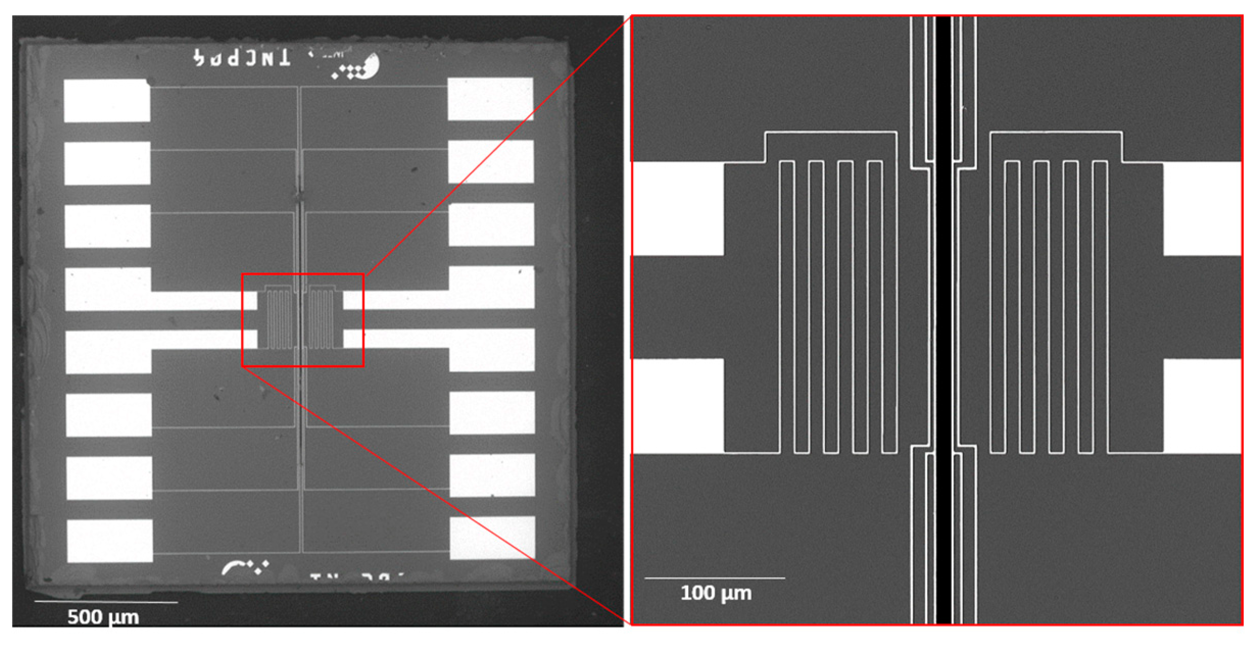
Our TNCP is an “early processed platform”. It is made via silicon micromachining and employs a central, thin silicon membrane with embedded resistive heaters, contact electrodes and Pt temperature sensors (
Figure 1). A narrow gap is separating the membrane in two halves to allow for thermal insulation and, thus, the generation of well-defined temperature gradients across the membrane. The nanowire under investigation is mounted across this gap and is electrically and thermally connected to four electrodes via focused electron beam induced deposition of Pt. (
Figure 2a). Meander-shaped resistive heaters, resistive Pt temperature sensors and contact electrodes, realized on both halves of the membrane, generate and control well-defined temperature gradients and will be used to measure resistivity and the Seebeck voltage of the nanowire. In addition, the whole TNCP chip is sized to fit into a TEM system for structural and chemical analysis of the nanowire.
A detailed discussion of the TNCP design and fabrication strategies can be found in [
9].
4. Experimental Analysis
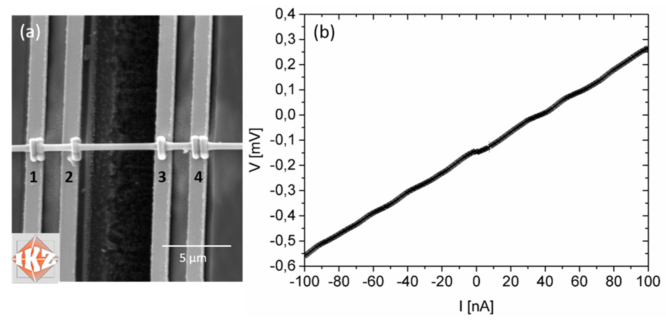
After checking the proper functionality of the TNCP, both in terms of electrical short circuits and/or circuit cut-off during fabrication, the nanowire is positioned across the gap on the membrane and over the measurement site. Platinum patches are applied by means of focused electron beam induced deposition (FEBID) to assure an ohmic contact between the nanowire and the four electrodes located on both edges of the gap (see
Figure 2a).
After sensor calibration, the thermovoltage can be measured at different temperature gradients along the nanowire, which reveals the Seebeck coefficient.
4.1. Nanowire Assembly and Contacting
The nanowire assembly is done utilizing a tungsten needle with a tip diameter of 10 μm and a cone tip radius of 0.1 μm. The nanowires are suspended in an aqueous medium and drop casted onto a rough silicon surface. The needle attached to a micromanipulator arm controlled by a strain gauge, under a high resolution optical microscope, enables finding, picking, and placing the intended nanowire onto the TNCP.
The electrical connection and mechanical fixing of the nanowire to the underlying electrodes is done in a SEM. For this purpose, a Pt-rich precursor gas is fed into the chamber. The focused electron beam cracks the injected precursor gas molecules, and as a result the Pt atoms deposit and generate Pt islands. The remaining volatile materials are pumped out of the chamber.
Figure 2a depicts a connected nanowire.
Resistance measurements are done on the isothermal TNCP in a four point configuration, in which current is applied to the outer electrodes 1 and 4, whereas the voltage drop across the nanowire is recorded with the inner electrodes 2 and 3 (see
Figure 2a). The resulting linear I–V diagram, shown in
Figure 2b, confirms the electrical contact between the nanowire and the electrodes. From the nanowire resistance and dimensional data (length = (6.33 ± 0.65) μm and diameter = (377 ± 5) nm) the electrical conductivity is extracted to be (1.38 ± 0.1) × 10
4 S/m at T = 285 K. This is calculated by assuming a round shape of the cross section.
4.2. Seebeck Measurement
The inner electrodes 2 and 3, shown in
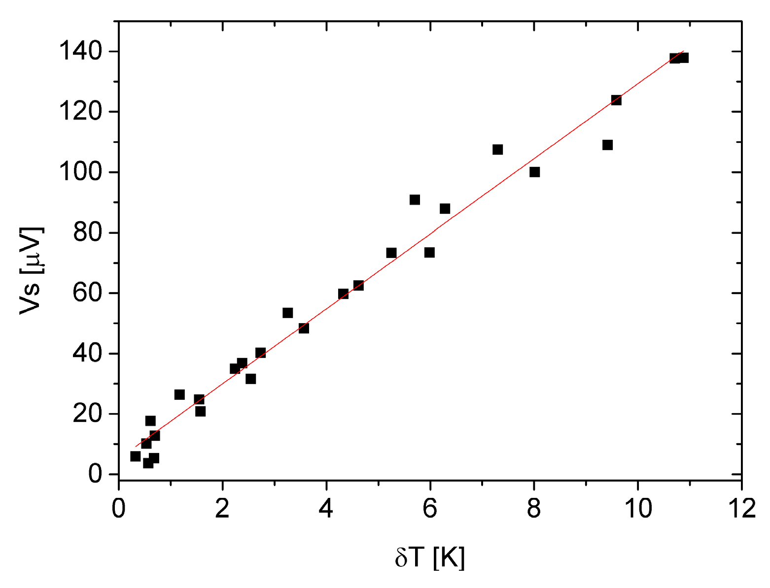
Figure 2a, are both resistive temperature sensors and thermovoltage collector electrodes, allowing for an accurate Seebeck coefficient measurement. After calibration of these sensors, a temperature gradient is generated over the nanowire via the resistive heaters left and right from the central gap (
Figure 1). The thermovoltage at the presence of different temperature gradients is measured in a He atmosphere (
Figure 3). A linear fit to the data gives a Seebeck value of S = (−12.4 ± 0.3) μV/K.
5. Discussion and Conclusions
According to Reference [
5], the electrical conductivity of a 31.4 µm long Bi
2Te
3 nanowire, from the same batch used here, is 2.0 × 10
4 S/m at room temperature. Our measured value of (1.38 ± 0.1) × 10
4 S/m for a nanowire of length (6.33 ± 0.65) μm is in agreement with this value.
In the literature it has further been reported that Bi
2Te
3 nanowires may show n-type or p-type behavior, evidenced by a positive or negative Seebeck coefficient. As reported in [
10], Seebeck coefficients obtained for several single Bi
2Te
3 nanowires range from (−87.5 ± 1.5) to (+135 ± 2) μV/K at room temperature. This large spread of the values for S is a result of the lack of control of the synthesis process, resulting, e.g., in slight variations of the stoichiometry from nanowire to nanowire. Our measured Seebeck coefficient is within this range of reported values.
To conclude, we have demonstrated the function of our TNCP by measuring the electrical conductivity and Seebeck coefficient. We have also shown a complete route for assembling nanowires onto pre-fabricated measurement platforms and for electrically contacting them. The platform realized is available as a “hand-out” to study other specimen or for using other experimental set-ups.
Acknowledgments
This study was supported by the German Research Association DFG (SPP 1386). Thanks to Martin Albrecht, the FEBID processes was performed in the Leibniz institute for crystal growth (Berlin, Germany).
Conflicts of Interest
The authors declare no conflict of interest. The founding sponsors had no role in the design of the study; in the collection, analyses, or interpretation of data; in the writing of the manuscript, and in the decision to publish the results.
References
- Hicks, L.D.; Dresselhaus, M.S. Thermoelectric figure of merit of a one-dimensional conductor. Phys. Rev. B 1993, 47, 16631–16634. [Google Scholar] [CrossRef] [PubMed]
- Eibl, O.; Nielsch, K.; Peranio, N.; Volklei, F. Thermoelectric Bi2Te3 Nanomaterials; Wiley: Weinheim, Germany, 2015. [Google Scholar]
- Jin, C.; Xiang, X.; Jia, C.; Liu, W.; Cai, W.; Yao, L.; Li, X. Electrochemical fabrication of large-area, ordered Bi2Te3 nanowire arrays. J. Phys. Chem. B 2004, 108, 1844–1847. [Google Scholar] [CrossRef]
- Hamdou, B.; Beckstedt, A.; Kimling, J.; Dorn, A.; Akinsinde, L.; Bäßler, S.; Nielsch, K. The influence of a Te-depleted surface on the thermoelectric transport properties of Bi2Te3 nanowires. Nanotechnology 2014, 25, 365401. [Google Scholar] [CrossRef] [PubMed]
- Schoenherr, P.; Zhang, F.; Kojda, D.; Mitdank, R.; Albrecht, M.; Fischer, S.F.; Hesjedal, T. Free-standing millimetre-long Bi2Te3 sub-micron belts catalyzed by TiO2 nanoparticles. Nanoscale Res. Lett. 2016, 11, 308. [Google Scholar] [CrossRef] [PubMed]
- Kojda, D.; Mitdank, R.; Handwerg, M.; Mogilatenko, A.; Albrecht, M.; Wang, Z.; Ruhhammer, J.; Kroener, M.; Woias, P.; Fischer, S.F. Temperature-dependent thermoelectric properties of individual silver nanowires. Phys. Rev. B 2015, 91, 24302. [Google Scholar] [CrossRef]
- Shapira, E.; Tsukernik, A.; Selzer, Y. Thermopower measurements on individual 30 nm nickel nanowires. Nanotechnology 2007, 18, 485703. [Google Scholar] [CrossRef]
- Wang, Z.; Moosavi, S.H.; Kroener, M.; Woias, P. Development of a Thermoelectric Nanowire Characterization Platform (TNCP) for Structural and Thermoelectric Investigation of Single Nanowires. In Thermoelectric Bi2Te3 Nanomaterials; Eibl, O., Nielsch, K., Peranio, N., Voelklein, F., Eds.; Wiley: Weinheim, Germany, 2015; pp. 253–281. [Google Scholar]
- Moosavi, S.H.; Kroener, M.; Woias, P. Cost effective MEMS fabrication of a nanowire characterization platform with solder coated electrodes. Sens. Actuators A Phys. 2016, 246, 140–147. [Google Scholar] [CrossRef]
- Beckstedt, A. Thermoelektrische Charakterisierung von Einkristallinen BiTe-Nanodrähten Thermoelectric Characterization of Single-Crystalline BiTe Nanowires; Hamburg University: Hamburg, Germany, 2013. [Google Scholar]
| Publisher’s Note: MDPI stays neutral with regard to jurisdictional claims in published maps and institutional affiliations. |
© 2017 by the authors. Licensee MDPI, Basel, Switzerland. This article is an open access article distributed under the terms and conditions of the Creative Commons Attribution (CC BY) license (https://creativecommons.org/licenses/by/4.0/).


