1. Introduction
Resistive solid-state gas sensors are very important electronic devices that have been developed in the last 4 decades due to their need in environmental and industrial air control. Their sensing principles are based on the variation of the resistance of a semiconductor material in the presence of certain gases [
1]. The materials typically used to fabricate these devices are metal oxide (MOX) semiconductors and the most accepted sensing mechanism is based on interaction of the surface O-atoms with the gas molecules, resulting in a change in resistance.
Currently, one of the investigation lines of this field aims at reducing the material’s dimensions. This miniaturization results in an increase of the surface-to-volume ratio and, consequently, a higher sensor response and a decrease in power consumption are expected. Different MOX nanowire (NW) materials can be used as sensing element [
2], among which Ga
2O
3 [
3] and In
2O
3 [
4] have demonstrate their efficient properties in gas sensing. The alloy of these two MOX, however, has been scarcely studied and no report is available on the gas sensing behaviour of this material.
The present work is focused on the growth of (Ga,In)2O3 nanowires by means of chemical vapour deposition (CVD), their structural characterization and their initial test as gas sensor.
2. Experimental
One of the techniques used in NWs synthesis is the so-called Vapor-Liquid-Solid (VLS) growth. It is based on a precursor of the NW material in gas phase that is incorporated to a drop shaped catalyst in liquid phase, forming an eutectic alloy. When supersaturation of the precursor in the alloy occurs, precipitation takes place, giving rise to the growth of the NW at the liquid-solid interface.
In our case, the precursor material is a mixture of Ga2O3 and In2O3 nanopowders, with graphite. A constant flux of carrier gas transports the vapor through the chamber where the Au (catalyst) sputter-covered Si/SiO2 substrates are placed.
Different mass ratios of Ga2O3:In2O3:C precursors have been used in this study to span different Ga-to-In compositions, which nominally are 9:1, 1:1 and 1:9 Ga-to-In atomic ratio. Graphite is used in this experiment to lower the evaporation temperature of the metal oxide precursor through the carbo-thermal reaction.
The experiments have been carried out changing the O2 proportion in Ar flow and the duration of the growth. The furnace temperature is also controlled at different zones, with the precursor boat maintained at 950 °C and the substrates, between 850 and 950 °C.
3. Results and Discussion
3.1. Scanning Electron Microscopy (SEM)
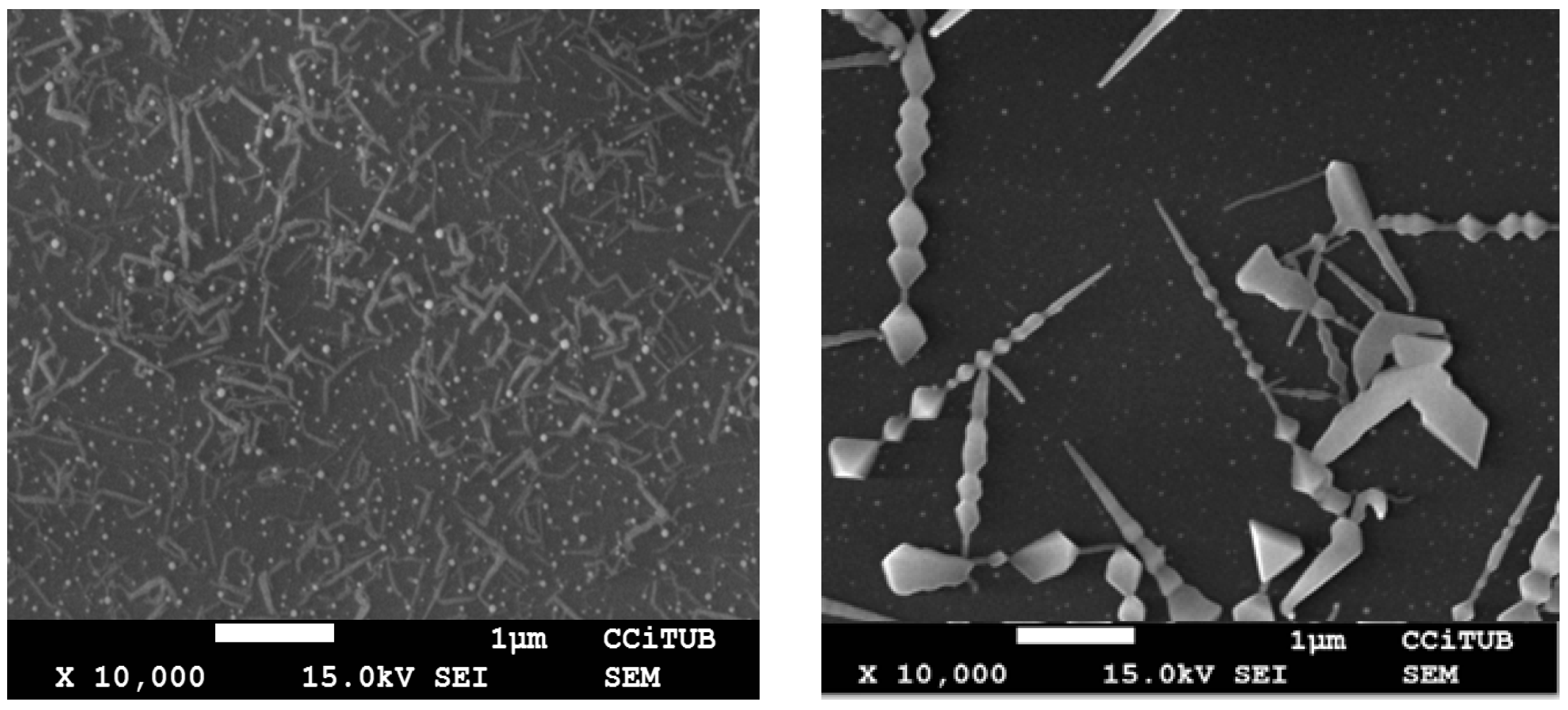
Figure 1 shows SEM images of samples grown under different conditions. In all of them the presence of NWs with lengths between 1 and 3 µm and diameters below 100 nm can be observed. The presence of the Au droplet at the tip of the NWs confirms that they are formed according to the VLS process.
In several samples, a coexistence of NWs and other structures can be observed such as nanorods (NR) and octahedral structures that can be interpreted as growing according to Vapor-Solid (VS) mechanism or as a combination of VLS and VS growth [
5].
3.2. X-ray Diffraction (XRD)
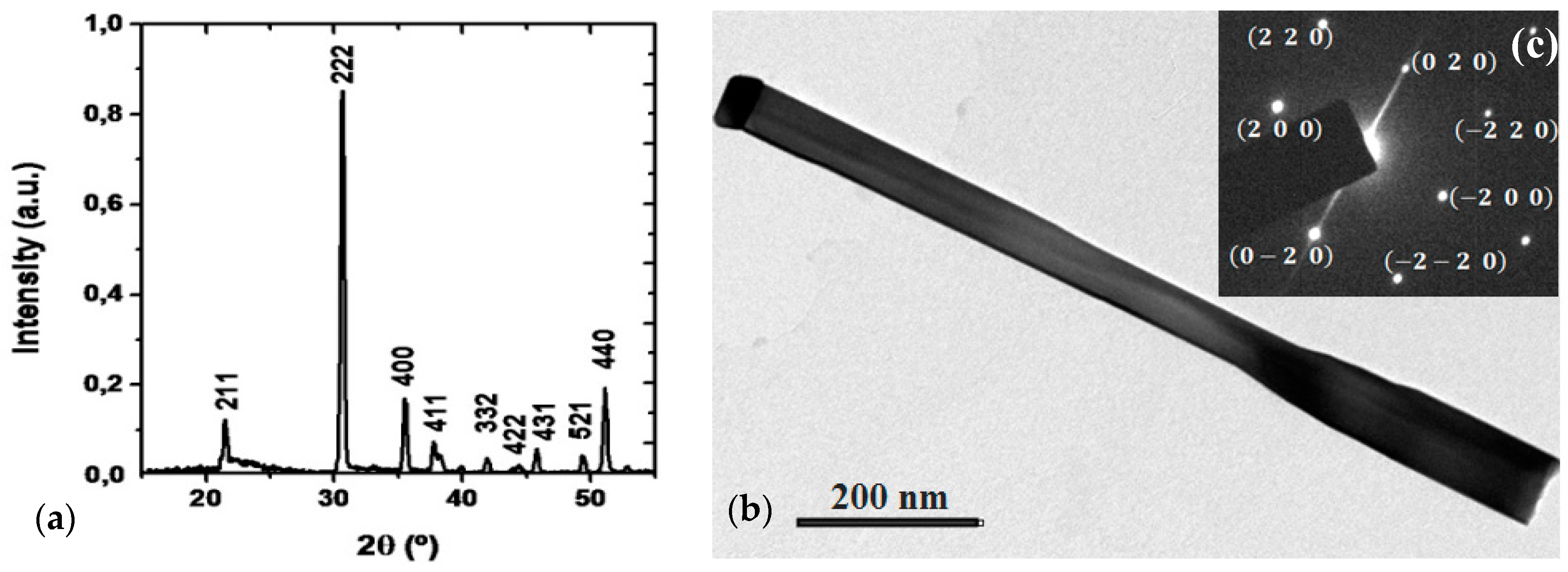
In order to analyze the crystallinity of the material, XRD analysis has been used with a grazing incidence (GIXRD) configuration has been used to maximizing the diffraction signal of the grown material.
Figure 2a, shows the XRD results of one of the grown samples. Comparing the obtained pattern with that of cubic In
2O
3, a good match is obtained, with only a small shift towards higher angles. This indicates that the NWs are mainly In
2O
3 material with a reduced introduction of Ga atoms in the lattice.
3.3. Transmission Electron Microscopy (TEM)
The TEM analysis corroborates the previous results obtained by XRD. The images shown in
Figure 2b,c have been taken both in image and diffraction mode, respectively. The presence of the Au tip in the NW, observed in
Figure 2b, confirms the VLS catalyst assisted growth of the NWs.
Figure 2c shows the corresponding diffraction pattern, which shows a regular diffraction spots distribution, proving that the NW is monocrystalline, the growth direction being [100].
4. Gas Sensing Behavior
In order to perform the gas sensor measurements, the grown material has been removed from the growth substrate and deposited on a microhotplate (MHP). The deposited NWs have been contacted using platinum Focused Electron Beam induced deposition [
6].
Prior to the gas sensing measurements, the calibration resistance-temperature curve has been measured for the contacted NWs. As expected, the sensor’s resistance decreases while the temperature increases, confirming the semiconducting nature of the NW.
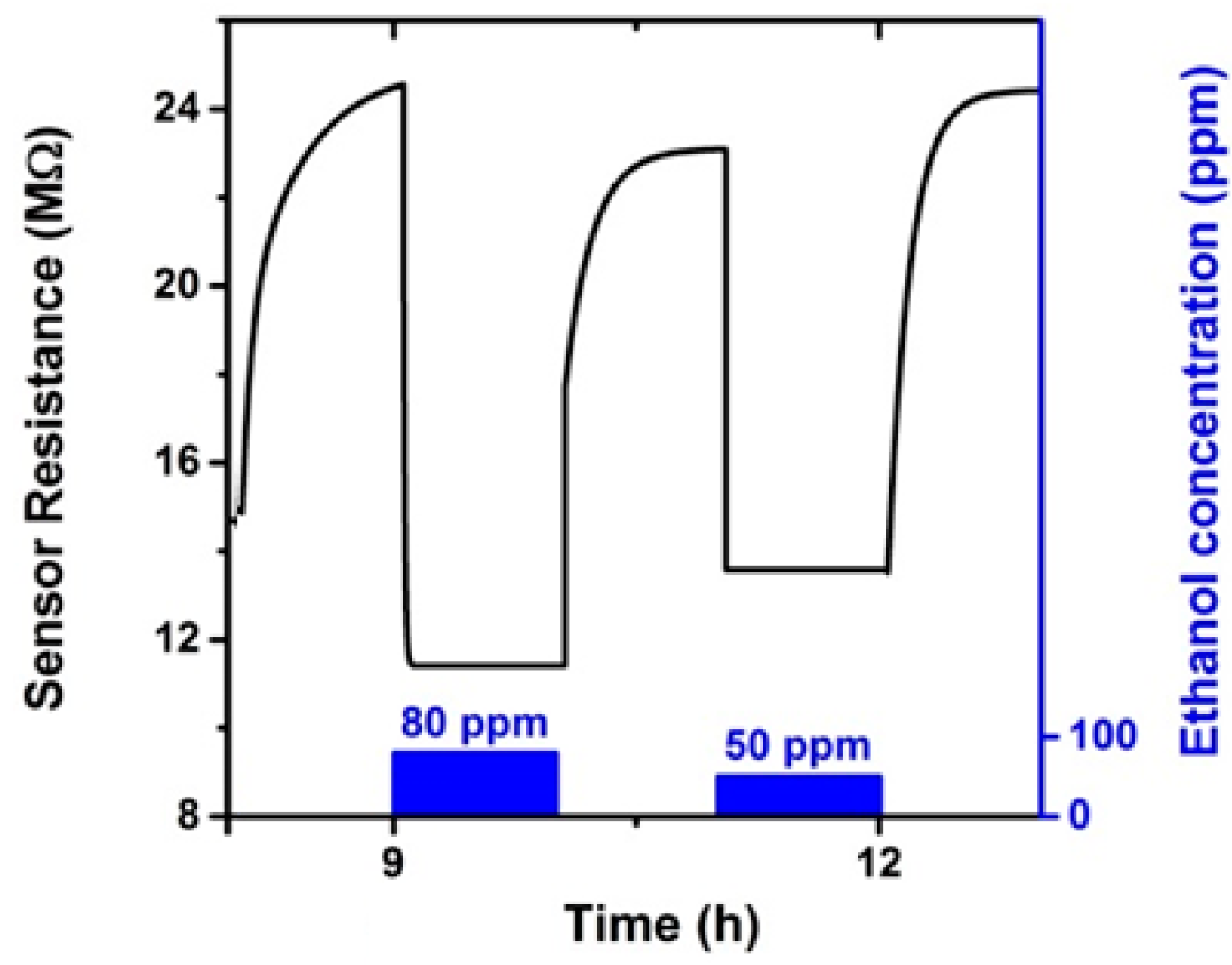
The response of the sensors has been tested towards ethanol gas diluted in dry synthetic air, as shown in
Figure 3 for the case of a temperature of 200 °C. The observed result, as to say the reduction of the resistance of the sensor in the presence of the gas, is in agreement with the reported reducing character of ethanol, whose change increases while increasing the ethanol concentration in the mixture. The sensor response goes from 35% to 80%. The recovery signal, however, is slow, indicating that the gas desorption process is the limiting parameter under these experimental conditions.
5. Conclusions
In this work, the growth of (Ga, In)2O3 NWs using the VLS mechanism has been carried out. Different mass ratios of Ga2O3-In2O3-C precursors have been used in order to obtain different stoichiometries in the NW’s structure. While changing the growth conditions, additional nanostructures, such as nanorods and octahedra, make their appearance thanks to the coexistence of VLS and VS growth mechanisms. The grown NWs are mainly crystalline cubic In2O3 with a small incorporation of Ga atoms. Preliminary tests of gas nanosensor based on single (Ga, In)2O3 NW on top of MHP show their effective response towards ethanol.

 ,
, 


