1. Introduction
SP (Surface Plasmons) are surface electromagnetic waves along a metal/dielectric interface. The real part of the dielectric constant of the metal must be negative, as in gold, silver o aluminum. For biological applications, gold is the most used metal due to the high control of interaction of this metal’s surface with alarge number of biochemical species that can be adhered to it. As there is no need of fluorescent markers, this technique is classified as label-free.
In the Kretschmann’s configuration [
1], the evanescent field of total internal reflection in the base of a prism can couple and excite Surface Plasmon (SP) at the substrate-metal interface. A second approach is the use of diffraction of light on a diffraction grating patterned on the gold layer. The diffracted wave excites a SP if the projection of the propagation constant matches that of the SP evanescent wave. This second technique does not need a prism nor the mechanical pressure system. The drawback is the necessity of fabricating a diffraction grating in where the prism setup uses a planar gold layer. The period needed for these grating require nanolithography techniques abricated.
Electron Beam Lithography (EBL) is suitable for prototyping nanostructured surfaces in an area of few mm2. The patterns are transferred sequentially by an electron beam to an electron-sensitive resist. After developing the resist, the metal can be etched by different means, resulting in the transfer of the designed pattern to the metal layer. Time and costs increase linearly with the size of the patterned area. In contrast, Laser Interference Lithography (LIL) exposes large surface at once, resulting in larger areas (about 1 cm2) and a much better cost-effectiveness. Similar to EBL, after developing, an etching process is needed to transfer the periodic pattern to the metal.
2. Materials and Methods
2.1. Fabrication Process
On a fused silica substrate, a 5 nm-thick Ti film is first deposited by sputtering as adhesion layer, followed by sputtered gold film, so the total metal thickness is 100 nm. Next, a 300 nm-thick AZnLOF 2070 negative photoresist is spun. In order to pattern the photoresist, a two laser beam interference set-up is used with a frequency-tripled Nd:YAG laser source (λ = 355 nm). The photoresist is prebaked for 60 s at 100 °C and, then, exposed to a single pulse of 8 ns and a fluence of 15 mJ/cm2 to obtain a 500 nm period grating. The sample is then postbaked at 110 °C for 60 s and developed in AZ-726 MIF developer (MicroChemicals GmbH, Ulm, Germany) for 20 s at 21 °C. Subsequently, it is immersed for 60 s in deionized water to stop the development process and, finally, dried with N2.
In order to transfer the periodic pattern from the photoresist to the gold layer, a Reactive Ion Etching (RIE) equipment was used with a non-reactive recipe: in an environment of 20 sccm of Ar, RF power of 173 W was used for 20, 30 and 40 s (chamber conditions: 20 °C temperature and 10 mTorr pressure). Trenches 250 nm wide with two different deeps were obtained over a circular area of approximately 1 cm
2. In
Figure 1a a photograph of the optical SPR-G sensor is shown, while
Figure 1b is a detailed SEM micrograph of the etched grating. The LIL technique has been previously used by the authors in [
2] for patterning diffraction gratings on Si
3N
4 and used as diffraction grating couplers also for optical biosensing purposes.
2.2. Instrumentation
Spectral interrogation has been used for characterization with a broadband source LS-1 and a spectrometer SD-2000, both from Ocean Optics, to measure the reflectivity of the SPR-G sensor [
2]. LS-1 is prepared for operating with fiber optics and the light is collimated and divided with a beam-splitter, being one of the beams TM polarized and focused using a 4× OLYMPUS objective. After reflection in the sensor, the light from the objective is focused in another fiber towards the spectrometer. The reflected spectrum is normalized to a reference spectrum measured in a flat area on the optical sensor, where there is no diffraction grating.
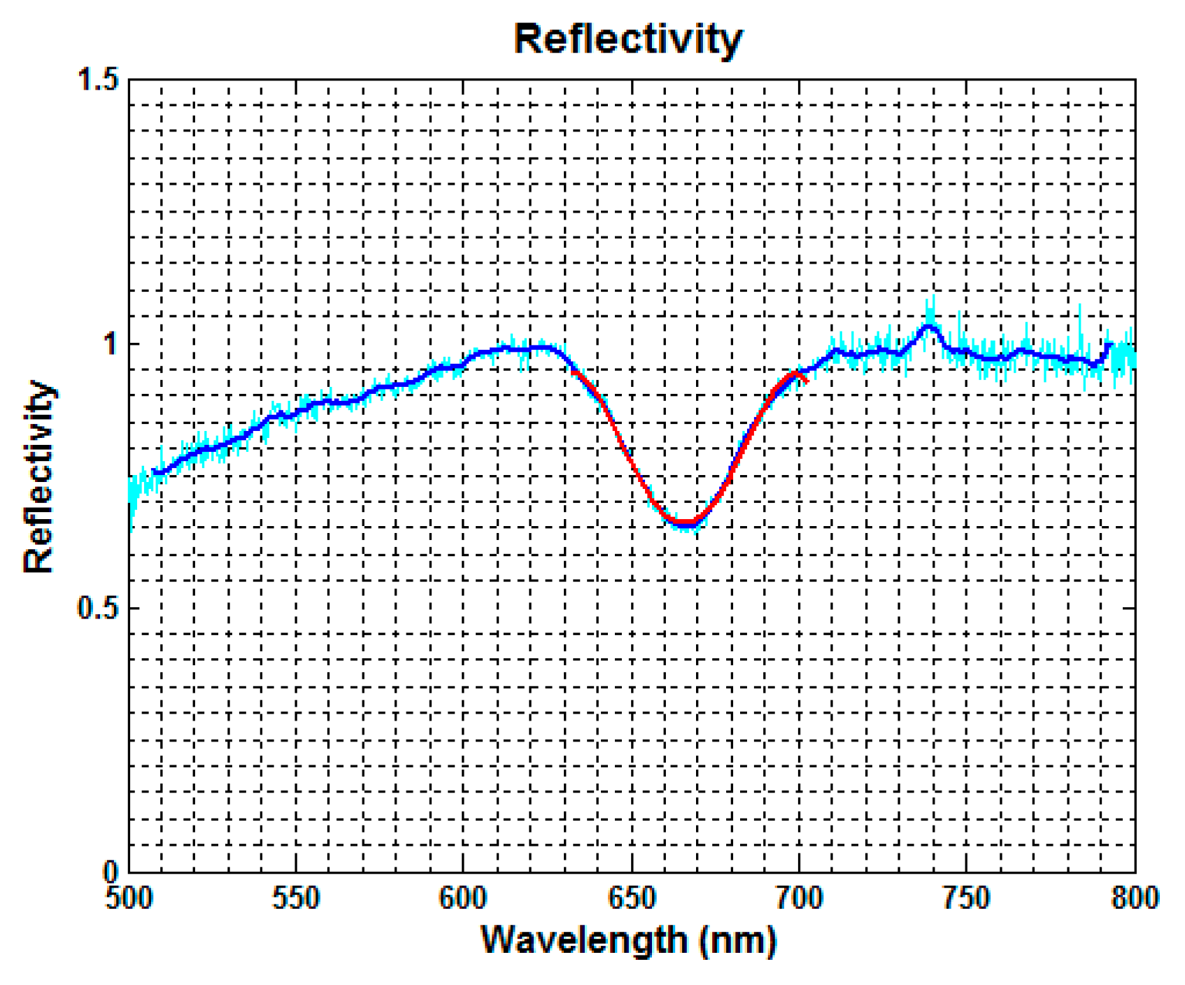
Figure 2 presents a typical reflection spectrum, showing the dip at about 670 nm as result of the resonance. In cyan the raw spectrum is showed, while the blue corresponds to the smoothed signal, calculated to reduce noise, which is further processed with MATLAB™ to find the minimum.
The base of the sensor is fixed to two MT3/M translation stages from THORLABS, for an X and Y scanning of the sensor. The movement is produced with two low-cost linear actuator stepper from CROUZET™, with a 10 mm displacement, and a commercial driver motor board (TB6560). The latter is controlled with the popular MSP430 microcontroller from TEXAS™, which is connected to a PC. The result is a low cost platform with a resolution of 8 μm in X and Y directions.
3. Results
3.1. Optical Characterization
Figure 3 is a 2D representation of the value of the resonance wavelength (left) and the depth of the resonance dip (right). In this case the measurement is done in steps of 200 μm and the sensor is covered with water. The blue spots correspond to flat areas of the sensor and they are fixed to λ
flat = 450 nm in order to have a proper contrast in the graph.
In
Figure 3 left, a small variation in the red tone at different points can be appreciated. The brighter red tone corresponds to lower wavelengths. The reason can be a non-uniformity of the grating depth at the different points. It seems that at the periphery of the laser spot the resonance wavelength decreases.
Figure 4 show two histograms obtained from the results of
Figure 3. The inner spots has a mean value of λ
inner = 695.4 nm ± 4 nm and in the periphery λ
outer = 678.1 nm ± 4.6 nm.
3.2. Bulk Characterization
In this section, we present the results of the characterization of the SPRG sensors under the presence of different liquids in order to obtain their bulk sensitivity.
Figure 3 and
Figure 4 are a particular case for water. The sensor is inside a fluidic chamber made of PDMS gasket and a top methacrylate cover. The system makes the X-Y scan of the surface, measures the spectrum at every position and finally calculates the statistics of the resonant wavelength.
Figure 5 is the result of the resonance wavelength for water (
n = 1.33), isopropanol (
n = 1.38) and glycerol (
n = 1.48), for two SPRG sensors with different etching times. The resonance represented is the mean value of the grating surface scanned, without taking into account the periphery or center of the grating. The slope of the fitted line is the bulk sensitivity, which is around of S = 387 nm/RIU for 100 s etching time and S = 354 nm/RIU for 60 s etching time. The mean resolution of the SD2000 spectrometer is around ∆λ = 0.3 nm, but a post processing allows lowering it to 0.01 nm, and then, a refractometric resolution of 2.7 × 10
−5 RIU is expected.
The sensitivity presents an excellent value but lower in front to other structures with plastic substrate, as S = 751 nm/RIU [
3]. From these results, it seems that shallower etching for a gold thickness of 100 nm is best, but this must be confirmed in future simulations with FDTD analysis.
4. Conclusions
In this work, the capabilities of LIL technique for rapid nano structuration of a large area of gold (around 1 cm2) and the possibility of its use as chemical sensor have been shown. We have developed a low-cost platform that can scan the surface of the sensor with a resolution of ∆x = ∆y = 8 μm. The best bulk sensitivity obtained for the SPRG sensors is around 390 nm/RIU.

 ,
, 


